HAL Id: hal-01004604
https://hal.archives-ouvertes.fr/hal-01004604
Submitted on 11 Jun 2014
HAL is a multi-disciplinary open access
archive for the deposit and dissemination of
sci-entific research documents, whether they are
pub-lished or not. The documents may come from
teaching and research institutions in France or
abroad, or from public or private research centers.
L’archive ouverte pluridisciplinaire HAL, est
destinée au dépôt et à la diffusion de documents
scientifiques de niveau recherche, publiés ou non,
émanant des établissements d’enseignement et de
recherche français ou étrangers, des laboratoires
publics ou privés.
Field plate termination for high voltage diamond
Schottky diode
Houssam Arbess, Karine Isoird
To cite this version:
Houssam Arbess, Karine Isoird. Field plate termination for high voltage diamond Schottky diode.
International Conference on Microelectronics ( ICM ) 2013, Dec 2013, Beyrouth, Lebanon. pp.25-28.
�hal-01004604�
Field Plate Termination For High Voltage
Diamond Schottky Diode
Houssam ARBESS
LAAS - CNRS, 7 avenue du colonel Roche, F-31400 Toulouse, France
Univ de Toulouse, LAAS, F-31400 Toulouse, France harbess@laas.fr
Karine ISOIRD
LAAS - CNRS, 7 avenue du colonel Roche, F-31400 Toulouse, France
Univ de Toulouse, UPS, LAAS, F-31400 Toulouse, France kisoird@laas.fr
Abstract— New field plate architecture is applied to pseudo
vertical diamond Schottky diode. New topology structure has been proposed and simulated using Sentaurus TCAD simulation in order to minimize the maximum electric field in the dielectric at high voltage operation. Firstly and after simple variations in the field plate architecture, the breakdown voltage was improved from 1632 V to 2141 V at 700 K. Concerning Emax in the dielectric, we obtained high decreasing
of the maximum electric field following the policy of pressure distribution.
I. INTRODUCTION
Power electronics based on silicon has now almost reached its limit (Operating temperature, high break down voltage limit, thermal conductivity, ...). To resolve this problem, there are two approaches: either by developing new component architectures, or turn to new semiconductor material able to function as desired. The first solution is in its operating limit. Thus we see new semiconductor material appear. The best known and most advanced are the gallium nitride for small and medium power application such as the automobile, or silicon carbide for medium and high power application. These semiconductors are at the industrial stage, the first SiC Schottky diode and JFET transistor are now commercialized.
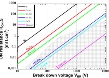
Fig. 1: Operating limits of silicon through the representation of the on-state resistance as a function of the breakdown voltage. In the non-exploitable
area, there is the wide bandgap semiconductors
Recently, diamond emerged as one of the best
considered to be the best material for power semiconductor devices due to its excellent material properties such as high breakdown field (>10 MV/cm), high mobility (4500 and 3800 cm2/Vs for electron and holes, respectively), low dielectric constant (5.7) and the highest thermal conductivity in the materials [1].
the interest of diamond obvious when reading Fig. 1. The compromise RON/VBR, which represents the ratio between the ON-resistance and the breakdown voltage of the device is excellent for diamond.
II. Issues
One of principal problems in diamond power device is the periphery protection. Indeed, the diamond has a high critical electric field, so, the junction termination structure is going to have a major impact in the OFF-state performance of the power devices. Without efficiency junction termination, strong field enhancement at the contact edge cannot be avoided, which causes premature avalanche breakdown of the device. The role of periphery protection is to distribute the electric field at the edge of junction or Schottky contact, thereby, increasing the experimental breakdown voltage. Several junction terminations have been explored for Schottky diodes in wide-bandgap semiconductors. Some of the more common ones are the guard ring [2], [3] the metal field plates extending over an insulating surface layer [4], [5], resistive Schottky barrier field plate (RESP) [6], and junction-termination extension (JTE) [7].
Due to difficulties associated with n-type doping in diamond and destructive effects of ion implantation on the diamond cristal, we focus the study in this paper to the Field plate termination due to the technological problems using other termination types.
Diamond is strong, which imposes severe constraints at the device termination. Since the critical field of the overall deposited dielectric material is less than that of diamond, we aim to find new architectures that reduce the electric field in the termination structure.
The critical field of the properties of diamond are close to the properties of best insulations available for power devices (epsilon, electric field, band gap, ...). It is therefore very difficult to use traditional material to realize junction terminations. Therefore it is a must to develop new protection architectures to reduce the maximum electric
All results shown in this paper were extracted at 700 K due to simulation problems at low temperatures. Other simulations have been made in order to evaluate the variation of maximum electric field with temperature shown a negligible difference.
III. PREVIOUS STUDY
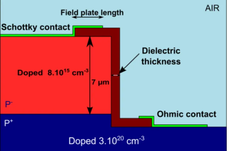
The previous structure studied at LAAS-CNRS is a diamond pseudo vertical Schottky diode with Field plate as termination on the diamond surface (Fig. 2). This structure consists of two diamond layers, the first is a 7 µm P+ doped diamond with boron concentration of 3.1020 cm-3 and the other is a 7 µm P- doped diamond with boron concentration of 8.1015 cm-3. To study the breakdown voltage of this structure and to look the optimum desired values of different technological parameters, we use Sentaurus TCAD simulation. The physical model used to calculate the breakdown voltage is the default Van Overstreaten model [8].
Fig. 2: Simulated pseudo vertical diamond Schottky diode
For this component, the field plate was optimized for a length of 10 microns and dielectric thickness of 0.7 microns. The dielectric used in this optimization is the Silicon oxide SiO2 [9]. With these parameters, we obtained 1638 V as a breakdown voltage. However the electric field reached at the end of field plate is higher than 19.9 MV/cm at 700 K.
IV. New topology structure and results
In a previous paper, new field plate architecture has been proposed. It is to keep the whole electrode flat, with no corners, and replace the diamond below the field plate region, with an optimized thickness of dielectric material (Fig. 3). The presence of corners on the path of the potential strengthens the electric field. In the first one (Fig. 2), the dielectric is located on the diamond surface, creating a corner in the electrode. At this corner the electric field is stronger in the diamond and then the impact ionization is greater for the first structure than the second for the same external voltage. Consequently, the breakdown voltage in the structure of Fig. 3 is higher than the structure of Fig. 2.
Fig. 3: New field plate architecture for diamond schottky diode
For the new field plate structure, the simulation with the same technological parameters of the new architecture component give a breakdown voltage equal to 2141 V. The chosen parameters are 10 micron for the field plate length and 1 microns for the dielectric thickness.
The highest electric field at 1700 V is 19.9 MV/cm for the initial structure and 19.8 MV/cm for the new one. The high mesh refinement in the high electric field zone (end of field plate) to 10 nm (node-to-node distance) shows an increase in the electric field to 49 MV/cm and 48.5 MV/cm for the initial and new architecture respectively. Assuming that the dielectric we used has a high quality, the maximum electric field carried by the silicon oxide is around 3 or 4 MV/cm. In this case, the oxide will break before the voltage across the diode reaches the maximum value, and consequently the field plate doesn’t play its desired function.
Looking at the experimental results, the average breakdown voltage was 400 V [9]. One of the reasons responsible for this failure may be the break of the dielectric. To improve the efficiency of the termination, we can change the dielectric as Ikeda [4], who used the Al2O3 as a dielectric for the field plate, but it's not enough. We aim to find a dielectric form for the field plate able to minimize the electric field as much as possible. Our idea is to change the topology of the structure including the field plate form. The maximum electric field is at the corner [6]. Thus, increasing the number of corners in the potential way, reduces the electric field value at the output of the field plate (distribution of peaks). Two architectures may be able to apply this idea.
a- The pillars dielectric form. That means, making the oxide in pillars form until the end of the electrode which increase the number of corners in the path of the potential
Fig. 4
(a).b- The graduated dielectric form
Fig. 4
(b).For these two terminations architecture, the efficiency depends on many parameters (field plate length, dielectric thickness, distance between pillars (Fig. 4(a)), distance between graduation (Fig. 4 (b)). Two dimensions
simulations have been made for the two architectures with two different dielectrics, silicon oxide and aluminum oxide, with variable thicknesses of dielectric.
Fig. 4: Pillars dielectric form (a), graduated dielectric form (b)
Fig. 5: Maximum electric field at 1700 V in terms of pillars height for the pillars dielectric form (a), and in terms of one step height for the graduated
dielectric form (b) for both SiO2 and Al2O3 as dielectric
Fig. 5 presents the maximum electric field at 1700 V for the two proposed field plate architectures, in terms of pillars height for the pillars dielectric form (a) and in terms of one
step height for the graduated dielectric form (b), for both SiO2 and Al2O3 as dielectric. Using the aluminum oxide (
ε
≈ 9) the maximum electric field is smaller than using the silicon oxide as dielectric. Emax decreases from 50 MV/cm to around 30 MV/cm. This minimum value is much larger than the maximum value supported by the dielectric (silicon oxide or aluminum oxide).A new idea consists to associate the two proposed structures described previously in order to increase maximum the number of corners without increasing the steps number. Fig. 6 presents this field plate architecture. A simulation shows that the maximum electric field at 1700 V equal to 22.7 MV/cm using the silicon oxide as dielectric and 16,5 MV/cm using the aluminum oxide as dielectric. Fig. 7 Presents the cross sectional view of the electric field for each graduation and at the oxide surface using aluminum oxide as a dielectric. This figure shows also the distribution of the electrostatic potential lines in the different zones of the structure.
Fig. 6: mixed form for Schottky field plate
Fig. 7: cross sectional view of the electric field for each graduation and at the oxide surface
Returning to the experimental result of Thion [9], a simulation with the same parameters of the experimental device and the same meshing strategy of the above components has been made. The results show that the maximum electric field equal to 18 MV/cm at 400 V. With this result, it can be deduce, the used dielectric (silicon
25 30 35 40 45 50 55 60 0 0,4 0,8 1,2 1,6 2 Ma x e le ct ri c fi e ld ( MV /c m ) Pillars height (µm) SiO2 Al2O3
(a)
25 30 35 40 45 50 55 60 0 0,4 0,8 1,2 1,6 2 Ma x e le ct ri c fi e ld ( MV /c m ) Oxide step height (µm) SiO2 Al2O3(b)
0 2 4 6 8 10 12 14 16 18 40 50 60 70 80 90 100 E ( MV /c m ) X (µm) First gradua:on Seconce gradua:on Third gradua:on Fourth gradua:on Oxide surface 1 2 3 4 5 1 2 3 4 5oxide) can support this electric field value that is focalized in a very small surface.
Based on this assumption, simulations of 3 proposed periphery protections have been realized with new break criteria, which is an electric field equal to 18 MV/cm. The dielectric used for those simulations is the layer of 1.6 µm of silicon oxide
Results show a breakdown voltage equal to 860 V and 896 V for components of Fig. 4 (a) and Fig. 4 (b) respectively and 1350 V for component of Fig. 6.
V. Discussion
Each proposed solution allows decreasing the peak of electric field, but not in the target range. Also we must consider other ways.
Replacing the silicon oxide with another dielectric material with higher electric permittivity (such as aluminum oxide Al2O3) reduces the value of the maximum electric field. However, the reached value remains above the requirement. In the final study of this paper, the simulation of the Thion structure [9] using the same mesh we made in this paper shows that the maximum electric field equal 18MV/cm. It can be say, since the maximum electric field is distributed in very small area (10 to 100 nm) , the critical field can be larger than in capacitor case.
A new study with high permittivity material is in progress.
VI. Conclusion
New field plate architecture for diamond Schottky diode was proposed which helps in increasing the breakdown voltage from 1632 V to 2141 V using the same technological parameters.
The maximum electric field in the field plate provokes a new problem since it is larger than the critical field of dielectric used. To resolve this problem, several solutions were proposed. The first is to make the field plate in a pillars form, the second is to change the field plate to graduated form and the last is making a mixed oxide form in order to increase the corners numbers. For all solutions, two dielectric material were used. The first one is the silicon oxide and the second one is the aluminum oxide.
VII. Acknowledgements
This work has been sponsored by the international associated laboratory (LIA) within the Framework of the project DIAMONIX II.
VIII. references
[1] R. S. Sussmann, CVD Diamond for Electronic Devices
and Sensors. John Wiley & Sons, 2009.
[2] S. K. Gupta, N. Pradhan, C. Shekhar, et J. Akhtar, « Design, Fabrication, and Characterization of Ni/4H-SiC (0001) Schottky Diodes Array Equipped With Field Plate and Floating Guard Ring Edge Termination Structures », IEEE Trans. Semicond. Manuf., vol. 25, no 4, p. 664 672, 2012.
[3] K. Ueno, T. Urushidani, K. Hashimoto, et Y. Seki, « The guard-ring termination for the high-voltage SiC Schottky barrier diodes », IEEE Electron Device Lett., vol. 16, no 7, p. 331 332, 1995.
[4] K. Ikeda, H. Umezawa, N. Tatsumi, K. Ramanujam, et S. Shikata, « Fabrication of a field plate structure for diamond Schottky barrier diodes », Diam. Relat.
Mater., vol. 18, no 2 3, p. 292 295, févr. 2009. [5] M. C. Tarplee, V. P. Madangarli, Q. Zhang, et T. S.
Sudarshan, « Design rules for field plate edge termination in SiC Schottky diodes », IEEE Trans.
Electron Devices, vol. 48, no 12, p. 2659 2664, 2001. [6] M. Bhatnagar, H. Nakanishi, S. Bothra, P. K. McLarty,
et B. J. Baliga, « Edge terminations for SiC high voltage Schottky rectifiers », in , Proceedings of the 5th
International Symposium on Power Semiconductor Devices and ICs, 1993. ISPSD ’93, 1993, p. 89 94.
[7] D. Alok et B. J. Baliga, « SiC device edge termination using finite area argon implantation », IEEE Trans.
Electron Devices, vol. 44, no 6, p. 1013 1017, 1997. [8] « Sentaurus user guide A-2008.09 ». .
[9] F. Thion, « Conception de protections périphériques applicables aux diodes Schottky réalisées sur diamant monocristallin », INSA de Lyon, 2012.