Publisher’s version / Version de l'éditeur:
Applied Physics Letters, 98, 25, p. 251101, 2011-06-20
READ THESE TERMS AND CONDITIONS CAREFULLY BEFORE USING THIS WEBSITE. https://nrc-publications.canada.ca/eng/copyright
Vous avez des questions? Nous pouvons vous aider. Pour communiquer directement avec un auteur, consultez la première page de la revue dans laquelle son article a été publié afin de trouver ses coordonnées. Si vous n’arrivez pas à les repérer, communiquez avec nous à [email protected].
Questions? Contact the NRC Publications Archive team at
[email protected]. If you wish to email the authors directly, please see the first page of the publication for their contact information.
NRC Publications Archive
Archives des publications du CNRC
This publication could be one of several versions: author’s original, accepted manuscript or the publisher’s version. / La version de cette publication peut être l’une des suivantes : la version prépublication de l’auteur, la version acceptée du manuscrit ou la version de l’éditeur.
For the publisher’s version, please access the DOI link below./ Pour consulter la version de l’éditeur, utilisez le lien DOI ci-dessous.
https://doi.org/10.1063/1.3600777
Access and use of this website and the material on it are subject to the Terms and Conditions set forth at
Selective-area vapor-liquid-solid growth of tunable InAsP quantum dots
Dalacu, Dan; Mnaymneh, Khaled; Wu, Xiaohua; Lapointe, Jean; Aers, Geof
C.; Poole, Philip J.; Williams, Robin L.
https://publications-cnrc.canada.ca/fra/droits
L’accès à ce site Web et l’utilisation de son contenu sont assujettis aux conditions présentées dans le site LISEZ CES CONDITIONS ATTENTIVEMENT AVANT D’UTILISER CE SITE WEB.
NRC Publications Record / Notice d'Archives des publications de CNRC:
https://nrc-publications.canada.ca/eng/view/object/?id=93b037c3-38cd-4881-9998-7b26f266cee5 https://publications-cnrc.canada.ca/fra/voir/objet/?id=93b037c3-38cd-4881-9998-7b26f266cee5Selective-area vapor-liquid-solid growth of tunable InAsP quantum dots
in nanowires
Dan Dalacu,a兲 Khaled Mnaymneh, Xiaohua Wu, Jean Lapointe, Geof C. Aers, Philip J. Poole, and Robin L. Williams
Institute for Microstructural Sciences, National Research Council, Ottawa K1A 0R6, Canada
共Received 19 April 2011; accepted 27 May 2011; published online 20 June 2011兲
A process is described where the position, size, and cladding of an InP nanowire with an embedded InAsP quantum dot are determined by design through lithography, processing, and growth. The vapor-liquid-solid growth mode on a patterned substrate is used to grow the InP core and defines the quantum dot size to better than ⫾2 nm while selective-area growth is used to define the cladding thickness. The clad nanowires emit efficiently in the range = 0.95– 1.15 m. Photoluminescence measurements are used to quantify the dependence of the excitonic energy level structure on quantum dot size for diameters 10–40 nm. 关doi:10.1063/1.3600777兴
The conventional approach to fabricating efficient single photon sources based on self-assembled quantum dots has been to use high finesse microcavities, taking advantage of the Purcell effect1 to efficiently channel photons from an excitonic decay into a resonant mode of the cavity.2 Re-cently, a highly efficient single photon source has been dem-onstrated in a photonic wire,3essentially an axial waveguide with a geometry similar to a small diameter micropillar cavity4 without Bragg mirrors. The devices are fabricated from a planar GaAs layer containing an ensemble of Stranski–Krastanow self-assembled InAs quantum dots using the standard top-down approach whereby the photonic wires are defined through electron beam lithography and dry-etching.
Quantum dots in nanowires, such as self-assembled dots, form a strongly confined system with narrow transition linewidths5,6useful for single photon7and entangled photon pair generation.8 Unlike self-assembled dots in etched pho-tonic wires, quantum dots in nanowires are grown, damage-free, from the bottom up via vapor-liquid-solid 共VLS兲 共Refs. 9 and 10兲 or selective area11,12 epitaxy. More importantly, each nanowire contains a single quantum dot which is natu-rally located on the axis of the nanowire for maximum cou-pling to the optical field of the waveguide.
For scalable implementations of nanowire-based single photon sources,8,13 VLS nanowires can be positioned using a standard metal lift-off process10 while positioning of selective-area nanowires is inherent to the growth mode.11,12 In this letter, we address two additional aspects for complete control of nanowire-based photonic wires; quantum dot size and cladding geometry. Using VLS epitaxy on a patterned substrate, the diameter of the catalyst is controlled through electron-beam lithography to better than ⫾2 nm. With the patterned-substrate, one can switch from VLS to selective-area growth, where the latter is used to clad the nanowire. The cladding of the nanowire is a crucial aspect of the device performance,13–15 and the approach adopted here can poten-tially be used to grow photonic wires with an optimal geom-etry for photon extraction.16
The nanowires are based on the InAs/InP material system. A 共111兲B S-doped InP substrate is coated with a
20 nm SiO2mask that is electron beam patterned to produce
an array of holes, 30 to 90 nm in diameter, that will define the gold catalyst size. The substrate is then wet etched in a buffered HF solution to produce openings in the SiO2 that
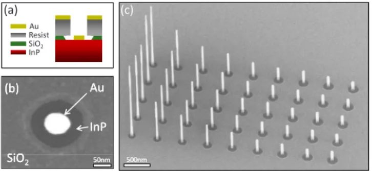
will define the cladding of the nanowire. The diameter of these holes is set by the etch time, with the isotropic HF etch producing an undercut profile shown schematically in Fig. 1共a兲. A standard metal lift-off process is used to deposit 10 nm 共samples A and B兲 or 1 nm 共sample C兲 of gold in the center of the opening in the oxide resulting in gold catalyst diameters of d = 20– 40 nm or d = 10– 16 nm, respectively, as measured after growth. A plan view scanning electron microscopy 共SEM兲 image of a catalyst prior to growth is shown in Fig. 1共b兲.
The nanowires are grown using chemical beam epitaxy with trimethylindium 共TMI兲 and precracked PH3 and AsH3.
The initial growth, which defines the quantum dot size, is carried out in the VLS mode at 450 ° C. At this temperature, InP grows exclusively at the gold–InP interface with no growth occurring in the annulus of exposed InP around the gold particle nor on the oxide-covered substrate17 as shown in Fig.2共a兲. The crystalline structure of all the InP nanowires were predominantly wurtzite 关see Fig. 2共b兲兴 with a growth rate-dependent stacking fault density. The VLS growth on patterned substrates is highly reproducible 关see Fig. 1共c兲兴
a兲
Electronic mail: [email protected].
SiO SiO Au Au InP InP InP SiO2 Resist Au (a) (c) (b) (b) SiO SiO22 50nm50nm 500nm500nm
FIG. 1. 共Color online兲 共a兲 Schematic illustration of the self-aligned lift-off process used to position gold catalysts in circular openings of a SiO2mask.
共b兲 Plan view SEM image of a positioned gold catalyst 70 nm in diameter prior to growth. 共c兲 SEM image of an array of InP nanowires where the size of the gold catalyst is increased from left 共d = 20 nm兲 to right 共d = 40 nm兲 with a corresponding decrease in height due to a nonlinear diameter-dependent growth rate.
APPLIED PHYSICS LETTERS 98, 251101 共2011兲
0003-6951/2011/98共25兲/251101/3/$30.00 98, 251101-1
with nanowire diameters controlled to ⫾2 nm. The size of the gold catalysts increases from left to right in nominally 2 nm increments with a corresponding decrease in nanowire height from the catalyst size-dependent growth rate.17InAsP quantum dots are incorporated at the base of the nanowires, 300–500 nm from the substrate surface, by switching from PH3to AsH3for two seconds. The quantum dots in sample A
were grown with a TMI flux during the AsH3 exposure,
while the dots in sample B and C were grown without TMI present. Figure2共a兲shows a 1 m nanowire with an InAsP quantum dot located roughly in the middle. Nanowires this tall are untapered, and the diameter of the gold catalyst is a good measure of the lateral size of the embedded quantum dot.
To grow the cladding, the growth temperature is raised to 515 ° C. At this temperature, the VLS growth mode is turned off and the noncatalyzed growth mode on the InP substrate is turned on.17Growth of the cladding material sim-ply proceeds by filling in the annulus around the nanowire core, the diameter of which is determined by processing. A clad nanowire is shown in Figs.2共c兲and2共d兲. The cladding extends half way up the nanowire, and reveals the crystalline facets of the wurtzite structure oriented along the 具110典 di-rections of the 共111兲 substrate. The diameter of the cladded region is d = 175 nm, lower than the optimal d = 250 nm based on calculations in Ref. 16 taking into account the lower index of refraction of InP compared to GaAs. The nanowires for optical study are grown sufficiently long to promote some tapering in the tip region due to finite indium diffusion lengths on the sidewall facets.17 The taper is an-other aspect in the design of an efficient device.16
Optical measurements on individual nanowires were per-formed at 5 K in a continuous flow helium cryostat using nonresonant, above band gap excitation through a micro-scope objective. The photoluminescence 共PL兲 is collected through the same microscope objective, dispersed using a single grating spectrometer and detected using a liquid-nitrogen cooled InGaAs diode array. After the PL measure-ments, the same nanowires are imaged in a SEM to
deter-mine the diameter of the gold catalyst which is used as a measure of the quantum dot lateral size.
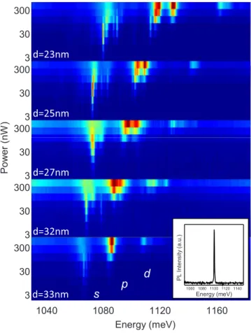
Figure 3 shows the power-dependent spectra of five nanowires with quantum dot diameters of d = 23 nm to d = 33 nm. For each nanowire, the ground state emission is a single peak with linewidths of a few hundreds of microelec-tronvolt. A typical spectrum pumped at saturation is shown in the inset of Fig. 3. The linewidth is 400 eV and the photon count rate is 500 cts/s, similar to InAs/InP self-assembled quantum dots. The spectra at higher pump powers display bound s, p, and d shells. As the dot size is decreased, the level spacings increase15 in accordance with increased lateral confinement. We emphasis that the quantum dot size is determined by design through lithography, and that the spectra in Fig.3 are obtained from adjacent nanowires posi-tioned in an array similar to that in Fig. 1共b兲with nominal 2 nm increments in the diameter of the quantum dot.
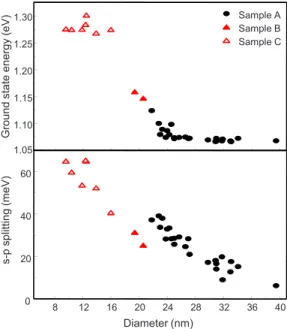
Ground state emission energies and s to p level splittings are plotted as a function of quantum dot diameter in Fig.4. For quantum dot sizes less than d ⬃ 24 nm, the ground state energy blueshifts with decreasing size at a rate of ⬃17 meV/ nm. A similar ground state dependence on quan-tum dot size has been previously observed.15 This trend is opposite to that expected from the known growth rate behav-ior as a function of nanowire diameter 共for sample A兲, de-scribed in Ref.17. The growth rate for a large diameter nano-wire is smaller than for a small diameter nano-wire, and thus larger diameter wires should have thinner quantum dots with a cor-responding increase in ground state energy. Countering this effect is the decrease in lateral confinement with increasing
5nm
(a) (d)
(c) (b)
100nm 100nm 400nm
FIG. 2. 共a兲 SEM image of a d = 40 nm InP nanowire prior to cladding. The nanowire is untapered, and the diameter of the gold catalyst is used as a measure of the lateral size of the InAsP quantum dot embedded at the base of the wire. 共b兲 Scanning transmission electron microscopy image of an InP nanowire with a wurtzite crystalline structure. 共c兲 and 共d兲 show a clad nano-wire in plan view and at 45°, respectively. The clad nanonano-wire has a diameter of d = 175 nm with clearly delineated faceted sidewalls.
n W ) d=23nm d=25nm 300 300 30 3 300 30 3 Po w e r (n d=27nm d=32nm d=33nm 1040 1080 1120 1160 Energy (meV) 300 30 3 300 30 3 30 3 1060 1080 1100 1120 1140 P L In te n si ty (a .u .) Energy (meV)
s
p
d
FIG. 3. 共Color online兲 Power-dependent emission spectra for a series of nanowires as a function of catalyst diameter. The diameters are obtained from SEM images of the measured nanowires. The inset shows the ground state emission of a d = 22.8 nm nanowire.
251101-2 Dalacu et al. Appl. Phys. Lett. 98, 251101 共2011兲
nanowire diameter but this is not strong enough to explain our results. For samples B and C there is no indium supplied during the AsH3 exposure and the dots are grown in the
manner explained in Ref.18. In that reference, when grow-ing InP the Au particle contained 44% In, and for InAs growth it contained 34% In. When switching from a P to an As ambient the extra 10% In in the Au particle was expelled through the growth of an InAs layer until a concentration of 34% was reached. This means that an InAs layer can be grown without injecting an indium source into the growth chamber. If a fixed change in In concentration in the Au particle is obtained then the thickness of the InAs layer will be directly proportional to the nanowire diameter. This is the correct trend for the behavior observed in our samples.
The splittings between the ground and first excited state as a function of quantum dot size are shown in Fig.4共b兲and are consistent with the results of Ref. 15. The observed in-crease in the s − p splitting for dein-creased diameters is ex-pected from a first order single-band approximation where the energy separation between s and p levels of quantum dots
strongly confined in the growth direction is determined by the lateral size of the dot.
In conclusion, we combine VLS and selective-area epi-taxy to grow InP nanowires with embedded InAsP quantum dots where the core wire and cladding thickness are defined independently by switching between growth modes. The quantum dot diameter is tuned in a controlled manner from 10 to 40 nm in 2 nm increments. The corresponding decrease in lateral confinement manifests in a decrease in the s to p level splittings, from 65 to 6 meV, illustrating the high level of control possible with nanowire-based quantum dots. The ability to control, by design, the nanowire position, diameter, and cladding thickness is relevant to the scalability, tunabil-ity, and emission efficiency, respectively, of nanowire-based photon sources.
1
E. M. Purcell,Phys. Rev. 69, 37 共1946兲.
2
A. J. Shields,Nat. Photonics 1, 215 共2007兲.
3
J. Claudon, J. Bleuse, N. S. Malik, M. Bazin, P. Jaffrennou, N. Gregersen, C. Sauvan, P. Lalanne, and J.-M. Gérard,Nat. Photonics 4, 174 共2010兲.
4
E. Moreau, J. M. Gérard, I. Bram, L. Manin, and V. Thierry-Mieg,Appl. Phys. Lett. 79, 2865 共2001兲.
5
N. Panev, A. I. Persson, N. Sköld, and L. Samuelson,Appl. Phys. Lett.
83, 2238 共2003兲.
6
M. H. M. van Weert, N. Akopian, U. Perinetti, M. P. van Kouwen, R. E. Algra, M. A. Verheijen, E. P. A. M. Bakkers, L. P. Kouwenhoven, and V. Zwiller,Nano Lett. 9, 1989 共2009兲.
7
M. Borgström, V. Zwiller, E. Müller, and A. Imamoglu, Nano Lett. 5,
1439 共2005兲.
8
S. N. Dorenbos, H. Sasakura, M. P. van Kouwen, N. Kopian, S. Adachi, N. Namekata, M. Jo, J. Motohisa, Y. Kobayashi, K. Tomioka, T. Fukui, S. Inoue, H. Kumano, C. M. Natarajan, R. H. Hadfield, T. Zijlstra, T. M. Klapwijk, V. Zwiller, and I. Suemune, Appl. Phys. Lett. 97, 171106
共2010兲.
9
R. S. Wagner and W. C. Ellis,Appl. Phys. Lett. 4, 89 共1964兲.
10
L. E. Jensen, S. J. M. T. Björk, A. I. Persson, B. J. Ohlsson, and L. Samuelson,Nano Lett. 4, 1961 共2004兲.
11
P. J. Poole, J. Lefebvre, and J. Fraser,Appl. Phys. Lett. 83, 2055 共2003兲.
12
P. Mohan, J. Motohisa, and T. Fukui,Nanotechnology 16, 2903 共2005兲.
13
J. Heinrich, A. Hugenberger, T. Heindel, S. Reitzenstein, S. Höfling, L. Worschech, and A. Forchel,Appl. Phys. Lett. 96, 211117 共2010兲.
14
M. Tchernycheva, G. E. Cirlin, G. Patriarche, L. Travers, V. Zwiller, U. Perinetti, and J.-C. Harmand,Nano Lett. 7, 1500 共2007兲.
15
N. Sköld, M.-K. Pistol, K. A. Dick, C. Pryor, J. B. Wagner, L. S. Karlsson, and L. Samuelson,Phys. Rev. B 80, 041312共R兲 共2009兲.
16
I. Friedler, C. Sauvan, J. P. Hugonin, P. Lalanne, J. Claudon, and J. M. Gerard,Opt. Exp. 17, 2095 共2009兲.
17
D. Dalacu, A. Kam, D. G. Austing, X. Wu, J. Lapointe, G. C. Aers, and P. J. Poole,Nanotechnology 20, 395602 共2009兲.
18
L. E. Fröberg, B. A. Wacaser, J. B. Wagner, S. Jeppesen, B. J. Ohlsson, K. Deppert, and L. Samuelson,Nano Lett. 8, 3815 共2008兲.
1.05 1.10 1.15 1.20 1.25 1.30 Sample A Sample B Sample C G ro u n d st a te e n e rg y (e V ) 20 40 60 -p s p lit ti n g (me V ) 8 12 16 20 24 28 32 36 40 0 20 s -Diameter (nm)
FIG. 4. 共Color online兲 共a兲 Ground state emission energy and 共b兲 s − p level splitting as a function of quantum dot diameter. The dots are formed by switching the PH3/AsH3out of/into the growth chamber simultaneously for
2 s, sample A with indium supplied, samples B and C without.
251101-3 Dalacu et al. Appl. Phys. Lett. 98, 251101 共2011兲