0 DOCUIEN'T ROMQ WIOMT ROOM 36-41Z]
R371LUCH ABC RAroRy C, F Ela2ThOICS !,7A P'lU( ivn'USTI IMTUTE F TFMOLOGT
AN
ANALOG DEVICE FOR SOLVING THE APPROXIMATION
PROBLEM OF NETWORK SYNTHESIS
R. E. SCOTT
C"
CD
'p
6, AL
TECHNICAL REPORT NO. 137
JUNE 8, 1950
RESEARCH LABORATORY OF ELECTRONICS
MASSACHUSETTS INSTITUTE OF TECHNOLOGYThe research reported in this document was made possible through support extended the Massachusetts Institute of Tech-nology, Research Laboratory of Electronics, jointly by the Army Signal Corps, the Navy Department (Office of Naval Research) and the Air Force (Air Materiel Command), under Signal Corps Contract No. W36-039-sc-32037, Project No. 102B; Department of the Army Project No. 3-99-10-022.
MASSACHUSETTS INSTITUTE OF TECHNOLOGY
RESEARCH LABORATORY OF ELECTRONICS
Technical Report No. 137 June 8, 1950
AN ANALOG DEVICE FOR SOLVING THE APPROXIMATION PROBLEM OF NETWORK SYNTHESIS
R. E. Scott
Abstract
An analog device has been developed which can solve the approximation problem of network synthesis with sufficient accuracy for most network problems. The complex frequency plane is represented by a conducting sheet of Teledeltos paper. The zeros and poles of the rational function are represented by positive and negative currents
introduced into the plane. The voltage along the j axis in the plane represents the logarithm of the magnitude of the rational function. This voltage is scanned by a
commutator at 10 cycles per second and displayed upon the face of a cathode ray tube. The locations of the poles and zeros for a desired function are obtained by a cut and try process.
A comparison of calculated and observed results shows that the accuracy of the device is 1-5 percent for the logarithm of the magnitude of the network function, and 3-15 percent for the phase, depending upon the particular function which is being solved. This accuracy is adequate for most network problems. A complete analysis is included of the errors introduced by the finite size of the plane, the finite size of the current and voltage probes, and the finite series impedance of the current sources.
AN ANALOG DEVICE FOR SOLVING THE APPROXIMATION PROBLEM OF NETWORK SYNTHESIS
INTRODUCTION
In this paper an analog device is described which provides a means of solving ex-perimentally the approximation problem of network synthesis. For many years the theory of synthesis of linear, passive, lumped-parameter systems has been known (1, 2). Practical applications of the general theory have lagged behind because of the difficulty of making suitable approximations. At the present time the necessary approximations are usually made by means of laborious cut-and-try methods. The same general procedure is used with the analog, (10, 11) but the time required is reduced from days to minutes. Thus, much of the tedious labor is removed from network synthesis and the designer can focus his attention on the more essential elements of a problem.
The Nature of Network Synthesis
Network synthesis can be described in general as the problem of designing an electrical network which will'produce a desired output response when a given input
stimulus is applied to it. A typical situation is illustrated in Fig. 1.
fl (tf) f2(t)
H(s) Fig. 1 The general synthesis problem.
FI(s) o F2(S)
In Fig. 1 the symbols are defined as follows: fl(t) the input stimulus to the network f2(t) the output response from the network
h(t) the output response for a unit impulse input
F1 (s) the frequency response of the input stimulus
F2(s) the frequency response of the output response
H(s) the frequency response of the network
s = a + j the complex frequency variable o- the damping factor
o the angular frequency
In the time domain the network is characterized by its impulse response, h(t). This function is related to the input, fl(t), and the output, f2(t), by the relatively
complicated convolution integral
o
-1-In the frequency domain the network is characterized by its frequency response H(s). This function is the quotient of the input Fl(s), and the output F2(s).
F2(s) = Fl(s) H(s) . (2)
The relative simplicity of Eq. 2 in comparison with Eq. 1 has led to the development of network synthesis in terms of frequency responses, rather than in terms of time re-sponses. If the data for a problem are given in the frequency domain, the procedure is straightforward. If they are given in the time domain the first step is usually to trans-form them to the frequency domain by taking a Fourier transtrans-form or its equivalent.
These two cases will be discussed separately.
Data Given in the Frequency Domain
In a great many problems of network synthesis the data are given directly in the frequency domain. Often they take the form of curves of the desired response as a function of the frequency w. These curves may arise as theoretically desirable forms, e.g. the flat amplitude response of a low-pass filter, or they may be derived from ex-perimental results, e.g. frequency compensation for an amplifier. The synthesis
pro-cedure when the data are in this form consists of two steps.
1. The approximation of the given curve by a function of o which can be realized by linear, passive, lumped-parameter elements
2. The calculation of the network elements from this function
It is the first of these two steps which is facilitated by the use of the potential analog which is described in this paper. There are relatively direct methods (3, 4) for accom-plishing the second step, and they will not be discussed here.
Data in the Time Domain
When the data are given in the time domain the designer has the choice of working directly in terms of time functions (5, 6) or of transforming the data to the frequency domain. This latter procedure is usually the most satisfactory, at least within the limitations of the present techniques for time domain synthesis. It may be carried out by Fourier series when the functions are periodic, and by Fourier integrals (or Laplace transforms) when they are not. The complete process is then
1. The conversion of the given data to the frequency domain 2. The approximation by a realizable function of X
3. An inverse transformation to the time domain to check on the tolerances of the approximation process
4. The calculation of the network elements from the approximate function
The approximation problem remains an essential element of network synthesis regardless of the original form of the data.
-2
The Role of the Approximation Problem in Network Synthesis
The approximation problem in network synthesis arises from the necessity of ex-pressing the network function H(s) in a form which can be realized by the physical net-work elements, resistors, inductors, and capacitors. To be physically realizable (7), H(s) must be a rational function of the form
A(s - s ) (s- s3)...
H(s) (s- s2) (s 4)... (3)
where A is a constant and s is the complex frequency variable.
The complex frequencies sl, s3, ... which make the numerator of H(s) zero, are
called the zeros of the function, and the complex frequencies s2, s4, ... which make
the denominator zero are called the poles of the network. The function H(s) is deter-mined by the locations of its poles and zeros in the complex frequency plane, to within a constant multiplier.
If H(s) is to represent the driving-point impedance of a two-terminal network the poles and zeros must satisfy the following additional requirements.
1. The poles and zeros must lie in complex conjugate pairs (or on the real axis). 2. The poles and zeros must lie in the left half-plane (in the limit they may lie on
the imaginary axis).
3. Poles on the imaginary axis must be simple and the residues must be real and positive.
4. The phase angle of the function along the imaginary axis must remain in the range -90 ° to +900 i. e. the poles and zeros on either axis must alternate.
If H(s) is the transfer impedance of a four terminal network, the above requirements may be relaxed a little.
1. The poles and zeros must lie in complex conjugate pairs or on the real axis as before.
2. The poles must lie in the left half-plane as before, but the zeros may be any-where.
3. Poles on the imaginary axis must be simple.
The network response obtained as the ratio of the required output response to the given input response (Eq. 2) will not in general have the form of the rational function
of Eq. 3. The approximation problem consists in finding a function of the required form which will approximate the desired function to a required degree of accuracy, and at the same time meet the requirements which have just been stated. Essentially the problem is one of finding a set of poles and zeros which meet the required condi-tions, and which approximate the desired function for s = j. An experimental method of obtaining the poles and zeros will now be described.
-3-The Use of Potential Analogs for Locating Poles and Zeros
The approximation problem can be solved analytically, but the amount of work re-quired is prohibitive. Fortunately, an experimental method is available for locating poles and zeros which will approximate any H(s). This method is based upon a potential analog which satisfies an equation similar to Eq. 3. If the logarithm of Eq. 3 is taken, the result is
lnH(s) =ln A +
E
is--S,-n
S-SnSn
+j arg (- sn) arg (- n)nodd neven odd n even
= G + j (4)
where G lnA + Is--
sn_
Is-sn1(5) n odd n even
=
A arg (s-sn)-
I
arg (s-sn) (6)nodd n even
G is the gain function of the network and is the phase function of the network.
From potential theory (see proof below) it is known that the voltage in a uniform conducting sheet has the same form as the gain function in Eq. 5, if positive currents are
introduced at points corresponding to the zeros, and negative currents at points corre-sponding to the poles. This analog may be used directly to approximate a given gain func-tion. The procedure is:
1. The required gain function is plotted.
2. Currents are introduced into the analog plane to represent the poles and zeros of the network.
3. The poles and zeros are arranged to give a voltage along the imaginary axis which has the same form as the required gain function.
If this procedure is followed the poles and zeros of the network will be obtained. To realize the full benefit of the analog, a number of additional requirements must be met.
1. The phase as well as the gain function must be available for observation. 2. The voltage along the imaginary axis must be plotted continuously, so that
the effect of changing a pole position will be instantly observable.
3. The magnitude of the errors introduced from all sources must be known and kept within reasonable limits.
These conditions are met by the analog device which is described on the following page.
-4-THE -4-THEORY OF -4-THE ANALOG
Prior to a description of the analog device a brief outline of the theoretical back-ground will be given. In the course of this derivation a method of obtaining the phase will be presented, and also a method of overcoming the errors introduced by the finite size of the analog plane.
The Derivation of the Analog Formulas
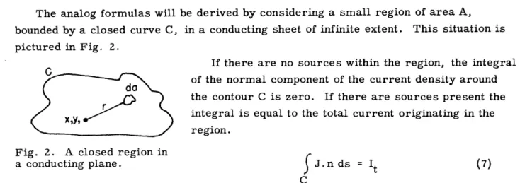
The analog formulas will be derived by considering a small region of area A, bounded by a closed curve C, in a conducting sheet of infinite extent. This situation is pictured in Fig. 2.
If there are no sources within the region, the integral r
of the normal component of the current density around the contour C is zero. If there are sources present the integral is equal to the total current originating in the region.
Fig. 2. A closed region in
a conducting plane. J. n ds = It (7)
C
For convenience it will be supposed that all the current sources within the region C have the same current I, and that they are distributed about the region in a continuous fashion with a density m. Outside the region C there are no current sources, and the boundary is remote enough so that it produces no effect within C. Then
jdiv
J da = m.I da (8)A A
or div J = mI (9)
But J = E _ grad 4
P P
where p = surface resistivity and
p
= potential.Hence div grad
4
= -mpI2
or v = -mpI . (10)
This is Poisson's equation. The solution for the conditions assumed here is (8).
(x,y) - p m rI (11)
A
where x, y, is any point in the region C
r is the distance from x, y, to the element of area da and r0 is a constant which sets the zero potential level.
-5-Equation 11 may be written
(x,y) = P I (m lnr da) -A (12) A
where A is a constant depending on the zero level only.
Instead of continuous distribution of currents we may now assume a finite distribution, with positive currents at the points s1, s3, ... corresponding to the locations of the zeros,
and negative currents at the points s, s4,... corresponding to the locations of the poles.
The point x, y, will be represented by the complex variable s, and the distance r, from any point sn will be Is - s. The current density m will be an impulse function, and the value of mda in the neighborhood of a zero will be unity, in the neighborhood of a pole, negative unity. Accordingly Eq. 12 becomes
¢,(s) P2I I ln Is-snl-
7
in Is-Snl- A · (13)n odd neven
Equation 13 is identical in form with Eq. 5 for the gain function of a network. The multiplying constant P - merely determines the scale factor of the result; the additive
constant A determines the zero level of the voltage, i. e. the impedance level of the gain function. Practical methods of determining these constants are discussed in Sect. 4.
Thus it has been shown that the voltage at any point in a conducting plane has the same form as the gain function, providing that positive and negative currents are introduced at the points corresponding to the zeros and poles of the gain function. The analog has been established under the restrictive assumptions of infinitely small probe size, and an
infinitely large conducting medium. The errors introduced by variations from these ideal conditions are discussed in Sect. 5.
The Phase Function
The logarithm of the impedance function is a complex function equal to
Gain + j Phase.
It is an analytic function and accordingly the Cauchy-Riemann equations hold. Thus
a
(Gain) = (Phase) (14)ao aw
and 00
Phase(Xo) = a Gain d · (15)
In the potential analog the gain is represented by the potential, and the phase is represented by the conjugate potential function, i. e. the current flow. If the phase is required at the point sl = 0l + j it can be obtained by integrating Eq. 15 along the line
( = l from o = 0 to = A. As an alternative the phase is the total current flow across the line joining s = o-l + j to the point s = a1. This method of obtaining the phase omits the
-6-900 phase shift which is produced by a pole or a zero at C = 1-l (at the origin, if the
phase is measured at real frequencies). In practice, it is a simple matter to take this into account.
At real frequencies the formula for the phase becomes
0
where K is a proportionality constant between gain function and the voltage and J is the current density normal to the jw axis.
Phase ( 1) = KI (16)
where Io is the total current flowing across the jw axis between the origin and the point at which the phase is being measured.
In the physical analog it is simpler to measure the voltage gradients at right angles to the jo axis and to integrate them to obtain the phase than it is to measure the total current flowing across the axis. For conceptual purposes however, the proportionality of the phase and the total current is particularly attractive.
Symmetry Conditions in the Potential Analog
Symmetry conditions in the potential analog can be used to simplify the construction of a physical device. Perhaps more important is the way in which they simplify the
conceptual background of the subject.
Symmetry About the Real Axis
Because of the conjugate nature of the poles and zeros, network impedances are symmetrical about the real axis. This means that in the potential analog the sources and sinks will be likewise distributed symmetrically with respect to the real axis. Thus, no current will flow across the real axis, and the plane may be cut along it without al-tering the voltage distribution in any way. Either half-plane by itself contains all the information which is required for the analog.
Poles and zeros right on the axis introduce a further consideration. The current from them would normally split half-and-half between the two half-planes, and ac-cordingly if only a single half-plane is used in the analog, currents introduced along the axis should be reduced to one-half of their normal value.
Symmetry About the Imaginary Axis
There is no symmetry about the imaginary axis in the original problem. But sym-metry can be created if the original problem is set up and simultaneously with it a problem which is its mirror image in the imaginary axis. Along the imaginary axis the voltage produced by each of these problems will be identical and the measured
-7-voltage will simply double. In addition, the axis. represents a saddle point for the sum of the two solutions, and this means that the measuring probes do not have to be so accurately positioned.
If the phase is being measured by means of the rate of change of voltage in a di-rection at right angles to the imaginary axis, some further changes are necessary. The required derivative is everywhere zero if the method of the preceding paragraphs is used. (Indeed this is the point of using the method. ) Reversing the currents in the probes representing the image problem gives a voltage gradient which is simply double the required one.
These results can be proved mathematically in the following fashion. Let the origi-nal impedance function be
Z(s)
=j,
as in Eq. 4.The logarithm of the magnitude of the impedance function is then the voltage measured along the axis
V =ln J- - s (17)
and the phase function is
7arg jW - Sj (18)
Magnitude
For the measurement of the logarithm of the magnitude of the impedance function, the image solution is added. This changes Z(s) to
)t - s s + sk
Z(s)' s + (19)
where the bar denotes the conjugate complex number.
Now the logarithm of the magnitude of the impedance function along the j axis is
In Z(j), = ln J 2k
= 2Zln | (20)
and the phase is 0. The result shows that the magnitude measurement is simply doubled and the phase is zero.
Phase
For the phase measurements the problem is set up in the same way except that the
-8-poles and zeros in the image solution are interchanged. Thus Z(s) becomes i (s- sk s + s.
z~~(s)" k J. (21)
s
sj
s-
s + Sk
The logarithm of the magnitude of the impedance function along the j axis is now zero and the phase is
2 arg j- s . (22)
jC - i
The result shows that the magnitude is zero, and that the phase is simply doubled. An interesting corollary follows from these results. When the magnitude function is measured with the added image solution, the current across the j axis is zero and the plane could be slit along it without changing the solution in any way. Accordingly, the logarithm of the magnitude of the impedance function is proportional to the voltage along the open circuited j axis.
When the phase is being measured, the voltage along the j axis is zero and a
conductor could be placed along it without altering the solution in any way. The current in this conductor at any point is the integral of the current density from the end of the conductor to the point. Thus, the phase is proportional to the current which flows along the short-circuited j axis.
These two concepts are very helpful in presenting an intuitive picture of the gain and phase functions of a network from the position of its poles and zeros.
A Conformal Transformation to Minimize Errors Due to the Finite Size of the Plane
An analysis of the errors incurred because of the finite size of the plane is given in Sect. 5. In the device which is being described here these errors are minimized by the use of a logarithmic transformation of the conducting plane(12).
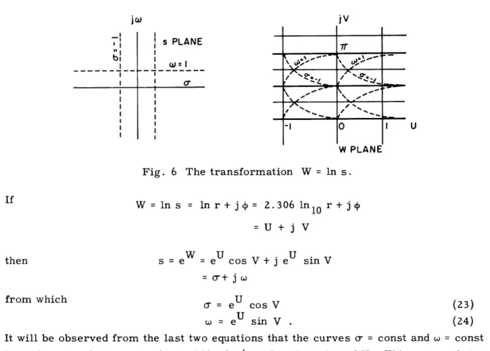
The transformation
W = n s = n r + j(O + 2n1r)
where s = re j and W = U + j V maps the whole s plane into a strip of width 2 in the W plane. The whole W plane thus corresponds to an infinite number of sheets in the s plane. A sketch of the transformation is given in Fig. 3.
s PLANE 1W IV w LANt S _ _ _ _ -47r 2wr -_-____ -_- -- Fig. 3 0 U In r The transformation -27r W = lns. -47r
-9-The problem of limiting the analog to a single. sheet in the s plane may be solved in the following manner.
1. Imagine that each sheet in the s plane has a distribution of poles and zeros. The configurations will be identical and they will all be symmetrical about the real
axis because of the nature of impedance functions. 2. Make the branch cut along the positive, real axis.
If these steps are followed, no current will flow from one Riemann sheet to the next. Accordingly, a single sheet may be set up to represent the analog. In the W plane,
this corresponds to two half-planes separated along the V = 0 axis, and with a sym-metrical distribution of poles and zeros repeated every distance of 2r in the V direction. Because of the symmetry, no current will flow across any line V = nTr. Thus, additional cuts may be made along any line V = n r without altering the distribution of potential, and a single strip of width r will represent the complete analog. (These additional cuts are not branch cuts. )
Advantages of the Analog
1. The finite-size problem is solved by the logarithmic nature of the coordinates. 2. A linear spacing of the probes may be used for both the gain and the phase. The
curves are then plotted against n (frequency).
3. The logarithmic coordinates are convenient for many problems. They correspond to the gain-phase analysis of circuits and log-db analysis of servomechanisms. 4. Calibration is simple using the ln-db techniques.
5. The accuracy is uniform over the useful region of the plane.
6. If a small area near each end is left unused, the errors due to the finite size of the plane will be negligible.
The advantages of the logarithmic transformation led to the construction of the physical analog in the logarithmic plane. In order to facilitate the operation of the device a conformal map of the original s-plane coordinates was printed on the conducting material in the logarithmic plane.
General Description of the Analog Device
The essential elements of the analog device are shown in the block diagram of Fig. 4. The conducting plane is a rectangular strip of Teledeltos paper which represents a semi-infinite strip in the logarithmic plane. Theoretically it should extend to infinity at both ends, but very little error is introduced by using a finite length and placing a conductor at each end, one to represent zero, and one to represent infinity in the logarithmic plane. The j axis from the s plane maps into a line along the center of the strip from one end to the other. The positive, real axis in the s plane maps as the bottom edge of the strip in Fig. 4.
CONDUCT(
AT ZERO
Fig. 4 Block diagram of the analog device.
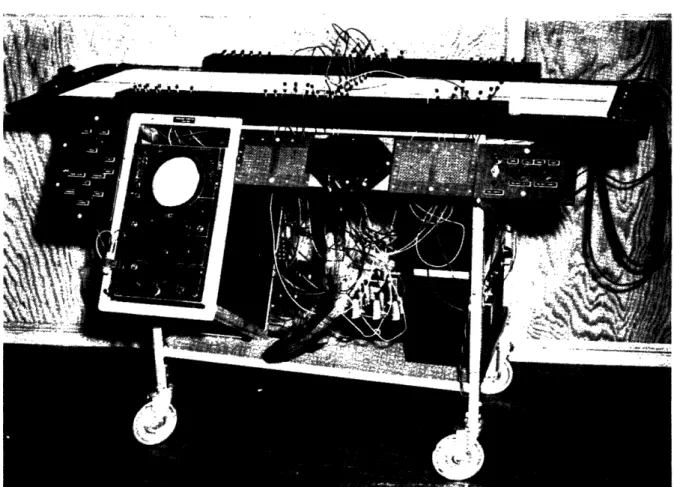
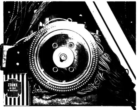
Fig. 5 The complete machine.
-11-Currents are introduced into the conducting plane by means of current probes. These probes are simply steel needles mounted in polystyrene holders. Ideally the sources feeding the current probes should be pure current sources. In practice this ideal is approximated by using 300 kilohms in series with each one, and a d-c source of either plus or minus 300 volts.
The voltage along the frequency axis is picked up by means of two rows of permanent probes. These probes are phonograph needles, mounted from beneath the plane so that only their tips come through the paper. Two rows are used so that both the gain and the phase function may be obtained. To obtain the former the average voltage of the probes in the two rows is used, and to obtain the latter the difference in voltage is used. There are 300 probes in each of the two rows and the commutator is capable of handling only one-third of these at a time. Hence a range switch is provided to select the three sections of the plane in turn. The output voltage from the commutator is amplified and displayed on the cathode ray tube for the gain function. For the phase function an extra stage of integration is required. The complete machine is shown in Fig. 5.
The Method of Operation
The method of operation of the machine is fairly simple. The desired form of the gain or the phase function is pasted upon the cathode ray tube and the poles and zeros are moved around from place to place in the conducting sheet until the picture on the cathode ray tube agrees with the desired one to within the desired tolerances.
In this manner the approximation problem of network synthesis can be solved in a few moments. The corresponding analytical procedure would require several days in many cases. Above all it should be noticed that problems requiring a large number of poles and zeros are handled in the analog with almost the same facility as the sim-plest problem. The same thing is not true at all of the analytical approach.
The Elements of the Machine The Teledeltos Paper
Teledeltos paper is a carbon-impregnated paper with a surface resistivity of about 4000 ohm-meters per meter. It has a current-carrying capacity of about 9 ma per
linear inch. (It burns at about 40 ma per linear inch.) The paper is fairly uniform. Deviations from uniformity and the errors introduced into the analog are discussed in Sect. 5. In the analog a strip of Teledeltos paper 55 inches long and 13.6 inches wide was used for the conducting plane. This size corresponds to a length of 10 inches per decade. This was chosen as a convenient value. It allows a plane of 5 decades in length without exceeding the size which could be handled on the printing presses in the Boston area. The three decades in the center of the plane represent the working space; one decade at each end is left free to minimize the errors due to the finite size of the plane.
The steps which were followed in printing the coordinate graph on the Teledeltos paper were
1. A template was made up which represented the curves a = const and o = const in the W plane.
2. A draftsman used this to produce one decade of the final graph.
3. This was photographed and duplicated to produce the required five decades. 4. Graphs were then printed on the paper by an offset process by the Buck Printing
Company of Boston. The Design of the Templates
The first step in the design of the template is to show that a single template will represent all the lines = const and = const in the W plane. For this purpose, the transformation W = In s is reproduced in some detail in Fig. 6.
i ijv -II I .. I bi uI bl s PLANE II I = 1I ._ I_ _ _ _
-O!
UFig. 6 The transformation W = In s.
W = n s = n r + j = 2.306 ln10 r+ j
=U+j V
W U U.
then s = e e cos V + j e sin V
-= + j co
from which = eU cos V (23)
w =e sin V . (24)
It will be observed from the last two equations that the curves a = const and = const have the same form except for a shift of /2 - V in the value of V. This means that the same template can be used for both curves. It is necessary merely to turn it over and shift its axis by 90° when passing from one curve to the other.
Finally it must be shown that all the curves of either family are of the same shape. For this purpose consider two curves
eU cos V = l (25)
eU sin V'= c2. (26)
The distance between the two curves on the real axis where V = 0 is
C2
U- U' = in cl . (27)
If this value is added to the value of U for curve one in Eq. 25, the curve will become identical to curve two of Eq. 26. Thus
U+lncl/c 2 e cos V = cl (28) becomes (29) e X Cos V c1 (29) or U e cosV = c2 . (30)
This equation is identical with the equation of the second curve, 26. This result shows that the second curve is exactly the same as the first except that it is displaced in the U direction by a distance in cl/c2.
The final conclusion is that a single template will represent all the curves in the W plane. The equation of this curve may be taken for the simple case of cl = 1. Then
U
e cos V = 1 (31)
1
U = loge cosV (32)
The curve of V against U can be calculated from this equation. The values must still, however, be converted to inches.
The scale factor is
10 inches = 1 unit of log1 0
= 2. 3026 units of loge .
Thus 1 unit of loge = 10/2.3026 = 4.343 inches and the value of V in inches = 4. 343
x (value in radians). (33)
1 The value of U in inches = 4. 343 X loge cos
= 4.343 X 2.3026 log10 1
= 10 log10 cosV (34)
To make the template, a graph of Eq. 34 was glued to a sheet of brass of 40-mil thick-ness. The brass was then cut out to this form, but slightly larger than required. The final shape was obtained by careful filing.
The next step in the process was the construction of the graph from the template. A draftsman used the template to produce one decade of the completed graph. For ease
in setting the template, a second template was constructed of a ten-inch logarithmic scale. This was used to determine the points along the axis where the curves were to start.
The final step was carried out by the Buck Printing Company of Boston. By a photographic process they made an offset plate which was five decades long, and from
this they printed the final graphs on the Teledeltos paper. This graph is plainly visible in the picture of the machine in Fig. 5.
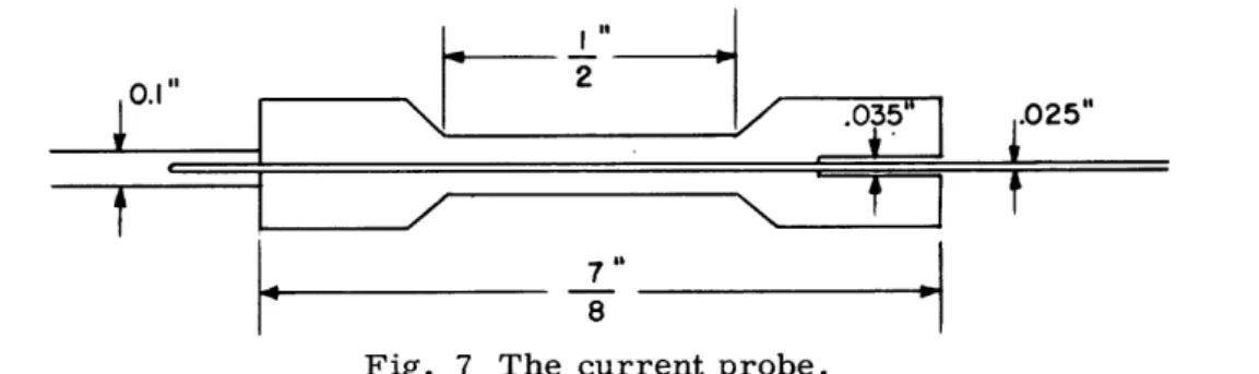
The Current Probes
The purpose of the current probes is to introduce positive and negative currents of constant magnitude into the conducting plane at specified positions. The method of constructing the current probes was evolved after considerable experimentation. The probe holders are made from a 7/8 inch length of 1/4 inch polystyrene rod. To make them easier to hold, the center 1/2 inch is turned down to 3/16 inch diameter. A hole, 0. 028 inch in diameter, is then drilled longitudinally through the rod. This diameter is sufficient to pass the steel needles which are to be used as the probes. One end of the hole is drilled out 0. 035 inch diameter to a depth of 1/4 inch. Then a 0. 034 inch sleeve is spot-welded to the needle. It is 1/4 inch long, and its position on the needle is 1/4 inch from the sharp end of the needle. In order to make a successful spot weld it is necessary to use a nickel sleeve.
The needle is fitted into the holder and a half-inch length of 0. 1 inch nickel tubing is spot-welded to the free end, thus securing the needle firmly in its mount. The wire which connects to the needle is soft-soldered to the free end of the 0. 1 inch tubing and an insulating shield is glued to the outside. Figure 7 shows the complete assembly.
OII1I 2..
0I" I N / nr-," ! w"
Fig. 7 The current probe.
The allowable current density in the Teledeltos paper is 9 ma for no heating, 40 ma for burning.
Steel needles are used to introduce currents into the plane. They have a diameter of 0. 025 inch. The corresponding total currents which they can carry are
I= x 0.025 X 9 = 0.8 ma for no heating = r X 0. 025 x 40 = 3. 5 ma for ignition.
From these results, the current chosen for the current sources was 0. 835 ma. This is about the maximum which can be used without running into nonlinear effects in the vicinity of the probes. However, it is worth noting that values greater than this can be used without introducing significant errors except in the neighborhood of the probes. This conclusion follows from the fact that the current from a probe is determined by the current source and will not be changed by a change in the surface resistance adjacent to the probe. Any other fields which exist in the plane will be distributed in this vicinity only.
-15-Poles and zeros at zero produce a uniform current flowing the full length of the plane in the logarithmic analog. For convenience in calibration, a switch is provided to introduce poles and zeros of any order at the origin.
Multiple order poles and zeros require currents in the analog plane which are multiples of the basic current. This follows from the fact that taking the logarithm of
an impedance function of the form
Z(s) = (s - sk)n
gives lnZ(s) = nln Is-skJ + j n arg(s-sk). (35)
Both the gain and the phase are multiplied by the order of the pole or zero. The corre-sponding result in the analog plane is obtained by multiplying the current emerging from the pole or zero by the order of the pole or zero.
Poles and zeros on the real axis have been split in two by the conformal mapping. That is, half of the current which would flow from them in the s plane flows in the upper half-plane and half flows in the lower half-plane. Only the upper half-plane is mapped into the logarithmic strip and so the current must be reduced by half for the probes on the axis. To accomplish this the series resistance for these probes is doubled.
It has been explained that the accuracy of the device is increased if the mirror image problem in the j axis is solved simultaneously with the original problem. It was also pointed out that the mirror image probes would have to have all their currents reversed in order to obtain the phase. In the analog there are two boxes of probes. One is used for the original solution and one for the image solution. The currents from the second box are automatically reversed when the device is switched from magnitude to phase.
The Voltage Probes
The logarithm of the magnitude of the impedance function is the voltage along the V = 90° axis in the W plane. A linear spacing of the voltage probes is used along this axis and, in conjunction with a linear sweep on the cathode ray tube, a plot of the logarithm of the magnitude of the impedance function against the logarithm of the frequency is obtained. Because of the necessity of making phase measurements, two rows of probes are used instead of one. They are on either side of the axis at a distance of 0. 05 inch from it.
The physical size of the probes was set by the size of phonograph needles which could be conveniently obtained. The diameter of the needles used is about 0. 025 inch. The number of probes which could be used per decade of the plane was set partly by the physical size of the probes, and partly by the fact that the commutator could handle only 100 lines at a time. For convenience, it was desirable that the commutator should scan one decade at a time. This set the number of probes per decade at 100 in each row, and the spacing between them at 1/10 inch since 1 decade is 10 inches in the analog plane. This value was actually the fundamental design parameter for
-16-the whole machine. The practical problem of setting -16-the probes in -16-the plane made -16-the 1/10 inch spacing very attractive. In addition, with the size of probes used, the error caused by the finite size of the probes is less than 1 percent (see below).
The usual procedure in operating the machine is to take the log magnitude function to be the average of the voltages on the two rows of probes. A switch is provided, however, which allows the operator to view the voltage on either set independently. If necessary, the plane may be shifted until the 90° axis lies along one of the rows of probes. In this case, the error introduced by the two-row system of measurements
can be reduced to zero. A discussion of the magnitude of this error is given below. It has been shown that the derivative of the phase with respect to the frequency is equal to the derivative of the logarithm of the magnitude of the function with respect to the damping ratio a. This relation held in the s plane. In the logarithmic plane, the derivative of the phase with respect to the real axis variable U, is equal to the derivative of the logarithm of the magnitude of the impedance function with respect to the imaginary axis variable V. The integral of this quantity with respect to the variable U is the phase as a function of U, (i. e. as function of log frequency). This integration is performed by means of an analog computor and the result is displayed on the cathode ray tube as phase vs. log frequency.
The slope of this curve is also of some interest and a separate switch is provided by which it may be viewed. It is related to the delay of the network; for
d 14)d do d= d S
= a q = 2ir f -W = w (36)
and d4/dw is the delay function of the network. The quantity which is measured on the analog plane is the derivative of the logarithm of the magnitude of the impedance func-tion with respect to the imaginary axis variable V. In order to measure this, two rows of probes are placed one on either side of the imaginary axis, and the voltage difference between them is measured. These discrete readings of the derivative are made into a continuous step curve by the commutator action, and the phase function is the integral of this curve.
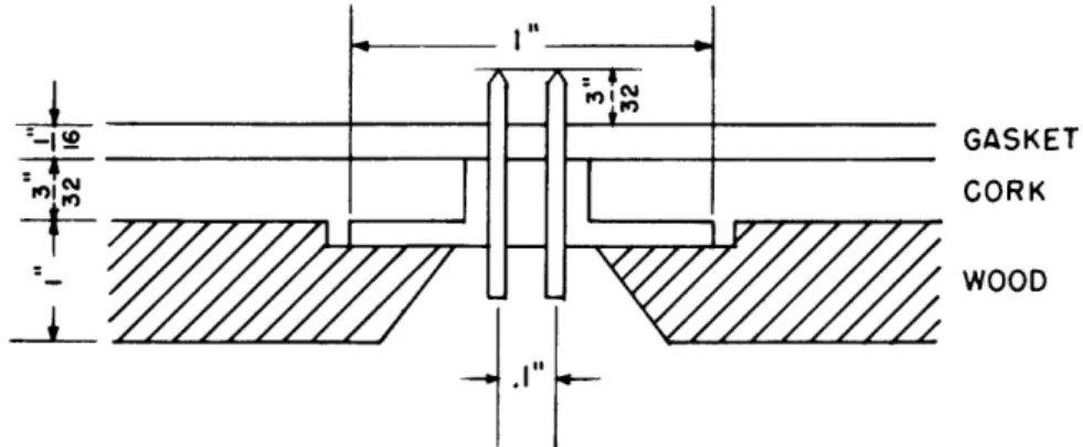
The voltage probes were constructed prior to the current probes. Steel phonograph needles were used instead of the steel needles, and they were held in place by means of a pressed fit in bakelite, rather than by a spot-welded sleeve. The main disadvantage of this method of construction was the difficulty of soldering the lead-off wire to the butt end of the phonograph needles. This was an extremely exacting and laborious task and it was not found possible to entrust it to a technician. A cross section of the mounting detail is shown in Fig. 8.
The phonograph needles are 5/8 inch long and about 0. 045 inch in diameter for the part which is embedded in the bakelite. (Because of the taper they are only 0. 025 inch where they enter the paper. ) The hole in the bakelite was drilled through with a No. 59 drill (0. 041 inch) and then the ends were reamed out with a 56 drill (0. 046 inch) to a depth of 3/64 inch. This was necessary to prevent splitting the bakelite when the
needles were forced into place.
The bakelite strip was milled to size, and then drilled while in place on the milling machine. This allowed the tolerance on the setting of any one hole to be held to about 0. 002 inch. The forced fit was also carried out on the milling machine, so that the tolerance on the vertical setting of the probes is also a few thousandths of an inch.
1
I
GASKET
CORK WOOD
Fig. 8 A cross section of the voltage probes.
The plane itself is of wood. The slot was cut on a circular saw, and the ledge to receive the bakelite member was chiseled out by hand. In the final assembly, the bakelite was glued to the wood. Before this step the solder connections were made from the separate probes to the terminal board below. This was necessary because of the delicacy of the probe to lead-off wire junction. When it is recalled that there are 600 of these junctions, and that they are spaced 0. 1 inch apart in two rows, it will be appreciated that this order of procedure was indeed necessary.
The Range Switch
The range switch is necessary because there are 600 voltage pick-up probes, and the commutator can handle only 200 at a time. For calibration purposes, it is con-venient to be able to look at a decade at a time, and so the division has been made in this fashion. The range switch consists of three sets of 200 female banana plugs which are connected to the probes in the respective decades of the plane, and a single set of 200 male banana plugs which is connected to the commutator. The general arrangement may be seen in the picture of the machine.
The female receptors are made from 3/32 inch bakelite strips, 7 inches 4 3/4 inches. Around the outside of each is a supporting shield of 5/32 inch brass, 1 inch wide, which adds necessary rigidity. The banana plugs are mounted in two square
10-by-10 arrays, with a center-to-center spacing of 1/4 inch between them. The male member is identical with the ones which have been described except that a square box has been built to cover the connections which are made to it. This provides pro-tection and at the same time a convenient handle when the switch is moved from one position to another. The bakelite pieces for the three female and the one male member were set up in a jig and drilled at the same time. This procedure was necessary to
-18-assure that they would be identical and fit properly when they were completed. The switch operates very satisfactorily, but it has been found advisable to add vaseline to the contacts to reduce the pressure required to insert and to remove the two hundred probes. When this procedure is followed, the switch may be moved from position to position with relative ease.
The Commutator
The purpose of the commutator is to scan the 200 probes in each decade at a linear rate. The output of the commutator is then applied to the vertical deflection plates of the cathode ray tube. A linear sweep is applied to the horizontal plates, and the
curve which results on the face of the scope is a plot of the voltage on the probes against the distance along the axis, or, in other words, the logarithm of the magnitude of the impedance function against the logarithm of the frequency.
The commutator is a mechanical one. It consists of a fixed member which contains the 200 contacts and two slip rings, and a rotating member which carries two copper brushes that make connection between the slip rings and the individual contacts. The individual contacts are connected to the probes through the range switch, and the slip rings are connected to the cathode ray tube through a buffer amplifier.
The picture in Fig. 9 gives the arrangement of the contacts in the stationary mem-ber. The circular contacts are brass fillet-head screws which have been countersunk in the bakelite support and faced off smooth in a lathe.
Fig. 9 The commutator.
The diameter of the screws is 1/16 inch. The diameter of the heads, as faced off, is 7/64 inch. The space between the contacts is 1/16 inch on the outer row, and 3/64 inch on the inner row. The radius at which the outer contacts are placed is 3 inches. The radius for the inner contacts is 2-3/4 inches.
The moving contacts were more difficult to design than the fixed ones. In their final form they consist of a "U" shaped strip of 15 mil beryllium copper. The depth of the "U" is 1/2 inch for both sets of brushes, and the width is 3/4 inch for the out-side one, and 3/8 inch for the inout-side one. The actual rubbing surfaces are coated with silver, which is soldered on to the copper. The area of the rubbing surface is just slightly larger than the area of a fixed contact. Thus wear is minimized and a very short dead time between contacts is achieved.
In order to prevent chatter it was necessary to make the spring constant of the brushes quite high. The resonant frequency is about 2000 cycles per second. At the speed at which the commutator is used (10 cycles per second, with 100 contacts) the fundamental vibration component occurs at 1000 cycles per second. With this ratio
of natural to applied frequency no damping has been found necessary, but when the speed is raised by any appreciable amount a rubber damper must be added to obtain satisfactory operation.
It has been found advantageous to lubricate the commutator with vaseline. This practice reduces the friction and helps to prevent wear of the bakelite. At the present time the commutator will operate satisfactorily for 10-15 hours with no attention. After this time, however, it needs cleaning and adjusting.
For protection a terminal board was mounted on the commutator, and permanent connections were made from the fixed contacts to the terminal board. The whole unit is removable, however, in order that it may be serviced with the greatest possible ease.
The addition of an extra contact to the rim of the rotating member provides a syn-chronizing pulse which is used to start the linear sweep on the cathode ray tube, and the linear sweep of the phase-slope control (see the buffer amplifier below).
The Buffer Amplifier and Integrator Unit
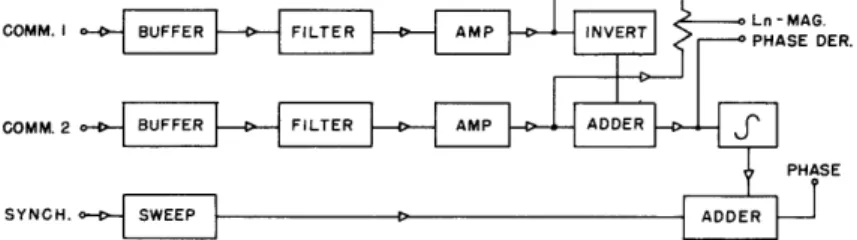
The buffer amplifier and integrator unit was designed to receive the voltages from the two channels of the commutator, and to deliver as outputs, the magnitude function, the slope of the phase function, and the phase. The magnitude function is the average of the two input voltages, the slope of the phase function is the difference of the two voltages, and the phase is the integral of this difference voltage. A block diagram of the system is shown in Fig. 10. The complete diagram appears in Fig. 11.
Before the details are explained, the overall operation will be discussed. The system is a novel one, in that it uses a-c amplifiers throughout and at the same time retains the full duty cycle. This effect is accomplished by performing the required operations on the ac components and on the dc components separately, and then adding
-20-the two components at -20-the output. For -20-the magnitude this involves merely -20-the addition of a constant term at the output. This operation is the equivalent of setting the zero db line on the cathode ray tube, and can conveniently be carried out on the cathode ray tube.
COMM. I
COMM. 2
SYNCH.
Fig. 10 Block diagram of the buffer amplifier and integrator unit.
For the phase the procedure is more complicated, since an integrated constant or a sweep wave must be added. The amount of sweep wave which must be added is deter-mined from the fact that the phase curve must be flat at very low and at very high frequencies.
In terms of the block diagram, the operation is as follows. In the magnitude posi-tion the inputs from the two commutators are identical. They are fed through buffer amplifiers and filters and then to a mixer tube in which the average of the two voltages is taken. This voltage is proportional to the logarithm of the magnitude of the impedance function. In the phase position the inputs from the two commutators are slightly dif-ferent. They pass through buffer amplifiers and filters as before, but one of them is then inverted and added to the other, thus giving the difference between them. This difference is the derivative of the phase function. Finally the derivative of the phase function is integrated and the necessary sweep wave is added, giving the phase. Each of the elements in the block diagram will now be discussed in detail.
The Buffer Amplifiers
The buffer amplifiers are cathode-followers which are shown as tubes 1 and 2 in the complete circuit diagram, Fig. 11. The input impedance of the circuit is about 10 megohms. The internal impedance of the probe source to which they are connected is
about 15, 000 ohms, and so there is very little loading on the circuit. The coupling capacitor in the input is likewise critical. If it is too small the circuit will lack the necessary low frequency response to pass the 10 cycle per second fundamental which is delivered by the commutator. If it is too large the commutator hash is accentuated. A value of 0. 05 ufd has been found experimentally to be a suitable compromise.
The Filter
The filter is designed to remove the commutator hash. The majority of the un-desirable signal occurs at the fundamental commutator ripple frequency of 1000 cycles per second. The filter is composed to two rejector circuits in series, both of which are tuned to approximately 1000 cycles per second, and an input capacitor which cuts
-21--4 10 D -i -22-__
down the high frequency response in general. The purpose of using two tuned circuits in series was to obtain the required impedance level with coils of relatively poor Q.
A switch has been provided which removes the filter from the circuit for testing purposes.
The Mixer Stage
A 12AU7 tube (No. 3) is used to mix the voltages from the two channels of the com-mutator. The tube is a double triode with separate cathodes, and each half is used as a cathode follower. The voltages which appear at the respective cathodes are the fil-tered voltages from the two separate channels of the commutator. By varying the set-ting of a potentiometer connected between these cathodes, the output voltage can be made the average of the two cathode voltages with any weighting factor that is desired. Thus the operator can view at will the output from either row of probes, or any combination of these outputs. Normally the outputs from the two rows of probes are equal and the potentiometer is in the center position to give a simple average.
The Inverter
An active inverter is used in order to provide the maximum of stability and inde-pendence of tube parameters. The feedback scheme has been described elsewhere (9)
and will not be discussed in detail here.
The amplifier for the inverter comprises tubes 10, 11, and 12 in the complete cuit diagram. The first tube is a high gain pentode, the second is a double triode cir-cuit that is equivalent to a cathode follower feeding a grounded grid stage, and the third is a cathode follower output. The requirements on the amplifier are stringent. It must have a high gain and a wide bandwidth, but it must not break into oscillations when large amounts of feedback are applied. In addition the output impedance must be low,
and the output must be 180° out of phase with the input. All these requirements are satisfied by the design used here. The amplification is about - 1000, the output im-pedance is about 100 ohms, and the bandwidth with feedback extends from about 1/10
cycle per second to about 200 Kc.
In order to prevent oscillations when the feedback is applied it is necessary to re-duce the bandwidth of the 6J6 stage to a few hundred cycles, from about 75 cycles per second to about 300 cycles per second. The overall bandwidth, however, remains large as shown by the data of the preceding paragraph.
The Adder
The principle of the adder is similar to that of the inverter. In the complete circuit diagram the adder is composed of tubes 4, 5, and 6. The two inputs are
1. The voltage from one of the rows of probes.
2. An inverted form of the voltage from the other row of probes.
Thus the output of the adder is the difference be-tween the voltages on the two sets of probes, a function which is proportional to the derivative of the phase curve (except for a possible constant term).
The Integrator
The principle of the integrator is not unlike that of the active adder and the active inverter. With a value of R = 1 megohm, and C = 0. 01 ufd, and the amplifier which
has been discussed above the finite-gain and bandwidth errors are of the order of 1 percent. This result has been checked experimentally with a square wave input.
In the complete circuit diagram the integrator is made up of tubes 7, 8, and 9. The input to the integrator is the voltage representing the slope of the phase curve. The output is proportional to the phase, except for the addition of the integral of a constant as explained at the beginning of this section.
The Phase Slope Generator
The phase slope generator is a standard thyratron sweep circuit. It is synchronized with the commutator by means of the same positive pulse which is used to start the linear sweep on the cathode ray tube. The thyratron is tube No. 16 in the complete circuit diagram. Tube No. 17 is an amplifier and inverter which produces sweep waves of opposite phase at its cathodes. The front panel control "phase slope" is a potentiometer between these cathodes, which can select either phase, and any amount of the sweep wave. The output from the potentiometer goes directly to the output phase mixer circuit, and also through a low-frequency compensation circuit to the grid of tube No. 18. The output from tube No. 18 is added to the phase in the phase mixer.
The Phase Mixer Circuit
The phase mixer circuit is composed of tubes 13, 14, and 15 in the complete circuit diagram. It is an adder circuit identical to the one which has been discussed previously. The inputs to this circuit are:
1. The phase minus the integral of any d-c components in the derivative curve.
2. A compensated sweep wave which replaces these lost components. The output of this circuit is the phase.
General Arrangement
The general arrangement of the machine can be seen in the picture in Fig. 5. Front panel switches are provided for viewing the Gain, the Phase, or the derivative of the phase. In addition a front panel switch allows multiple poles and zeros to be introduced at the origin.
Controls are also provided on the front panel for the magnitude of the sweep wave which is added to the phase, and for mixing the outputs from the two rows of probes in
any desired proportion when the Gain function is being viewed.
Two regulated power supplies supply the plus and minus three hundred volts which are required for the current probes. The buffer amplifier and integrator unit is sup-plied with power from the plus three hundred volt supply.
The Calibration and Operation of the Machine
The calibration procedures for the machine depend upon a knowledge of the charac-teristics of the so-called "log-db" type of curve. The output curves from the machine are in the form of Gain or Phase vs. log-frequency. These curves have been discussed
extensively in the literature (13), but a short summary will be given here of the results which are pertinent to the operation of the machine.
The "log-db" theory
Any impedance function Z(s) can be written in the form
A (TlS + 1) (...)(T 2 s2 + 2T2 2s + 1)(...
z(s) T2 2 (37)
(T3s +
1) (.
)(T4
s + 2T4t 4 s + 1)( ...Terms of the form (Ts + 1) are produced by single poles (denominator) or by single zeros (numerator) on the negative real axis. The quadratic terms are produced by pairs of conjugate poles or zeros. (If is greater than one the quadratic term is factored into two linear terms). If the logarithm of Z(s) is taken the result is
n Z(s) = nTl T1s + 1 +. 2 2T2 2 s + 1 +...
2 2
-In
T
3
s + 1 In T42 s2+ 2T44 s + 1-. (38)arg (Z(s)) = Arg(T s + 1) +... Arg (T2 s2 + 2T2 2 s + 1) +...
2 2 (39)
-arg (T3 s + 1)-... arg (T 2 s2 + 2T44 + 1)-...(39)
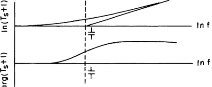
It is apparent from Eqs. 38 and 39 that the logarithm of the magnitude of the im-pedance function and the phase of the imim-pedance function are both obtained as the alge-braic sum of the contributions from terms of the form (Ts + 1) and (T2 s2 + 2T ts + 1). In the "log-db" method of analysis, the logarithm of the magnitude and the phase of these standard forms are recorded graphically. The form of the curve for (Ts + 1) is shown in Fig. 12.
The curve for the logarithm of the magnitude is asymptotic to the zero db line at low frequencies, and to a +6 db per octave line at high frequencies. The asymptotes meet at a frequency of 1/T, and at this point the actual curve is 3 db above the asymptotes. The curve for the phase is asymptotic to the zero phase line at low frequencies and to the 900 phase line at high frequencies. It is symmetrical about the frequency 1/T.
In the analog plane the term (1 + Ts) is represented by a zero on the negative real axis. In the W = n s plane this point is at the edge of an infinite strip. The current flows from the probe along the strip to a conductor at infinity. The voltage along the
C +, In I-01 , IInf I13 IT iT
Fig. 12 The "log-db" curves for the factor (Ts + 1).
axis is zero to the left of the probe, and it approaches a constant slope (of 6 db per oc-tave) when the current flow in the sheet becomes uniform at high frequencies. Thus the 6 db-slopes of the "log-db" theory are identified with a uniform current flow of one unit in the analog.
Terms of the form (T2 s2 + 2 T s + 1) have zero db log-magnitude asymptotes at low frequencies, and +12 db per octave asymptotes at high frequencies. The junction of the asymptotes is again the frequency 1/T. The exact behavior in the neighborhood of this point depends on the value of . Families of curves are plotted for various values of (ref. 10). The phase curves are asymptotic to the zero phase line at low frequencies and to the 180° phase line at high frequencies. They are symmetrical about the fre-quency 1/T, and have different slopes for different values of .
In the analog a term of the form (T2 s + 2T s + 1) is represented by a pair of con-jugate zeros at the points
- T T (40)
= 1 + j tan -1 1 (41)
Equation 41 shows that the radius at which the zeros occur is independent of the value of , and that the angle at which they occur is independent of the value of T. In the W plane, the position of the zeros along the strip is fixed by T, and the distance of the probes from the axis is fixed by . The current spreads out from these probes and flows along the strip towards infinity. The voltage along the V = 90° axis is zero to the left of the probes, and it approaches a constant slope (of 12 db per octave) when the
current flow becomes uniform in the sheet. Thus the 12-db slopes of the "log-db" theory are identified with a uniform current flow from a pair of conjugate probes in the analog. The distance between the probes and the 90 axis is associated with the damping factor .
Calibration of the Log-Magnitude Plots
The calibration of the frequency scale in the log-magnitude plot presents no diffi-culty. The commutator scans one decade at a time in the frequency scale, from a re-lative frequency of 1 to a rere-lative frequency of 10. The frequency scale therefore covers just one decade.
The calibration of the log-magnitude scale is accomplished by using the results above. In particular it has been shown that a single pole or zero has a "log-db" response which is asymptotic to + 6 db at high frequencies. If the pole or zero is located at the origin this slope exists throughout the whole frequency spectrum. The corresponding result is achieved in the analog by introducing a uniform current at the zero end of the W plane and allowing it to flow to the other end which represents infinity. The curve which is obtained may be used to calibrate the scale on the cathode ray tube. Examples of 0, + 6, and + 12 db slopes which were obtained in this way are shown in Fig. 13.
The infinite slopes shown in Fig. 13 provide a calibration for the vertical scale, but the problem of setting the zero db line remains. If there are no poles or zeros at zero, the asymptotic behavior at low frequencies is zero, and this fact determines the zero db line to within the constant A of Eq. 37. When poles or zeros are present at zero they can easily be removed for the purpose of calibration.
The limited range of the commutator also poses the problem of matching the curves obtained over two or three decades. The calibration is carried out as before in the decade nearest to zero, and the other decades are matched to it by adjusting the levels at the boundaries. An example of this process is shown in Fig. 14.
The Calibration of the Phase
The frequency scale for the phase is the same as the frequency scale for the log-magnitude, and requires no further calibration. The vertical scale for the phase plots is calibrated by measuring the phase of a single pair of conjugate poles, or zeros. The distance between the low and the high frequency asymptotes is 180° for conjugate probes
of either polarity. A calibration curve for the phase is shown in Fig. 15.
In the absence of poles or zeros at zero the phase curve has a low frequency asymp-tote of zero. The addition of poles or zeros at zero does not change the phase as it is measured on the machine. Therefore poles or zeros at the origin must be added into the calibration. A pole at the origin changes the calibration of the low frequency asymp-tote to -90 , and a zero at the origin changes it to +90° . Multiple poles or zeros change the calibration by multiples of 90° .
The Experimental Results
The experimental results which are presented in this section show the accuracy of the machine, and the scope of its operation. The first results are simply reproductions of the standard "log-db" curves for the quadratic factor (T2 s2 + 2T s +
1)-lwith various values of the damping ratio . The accuracy of the machine can be judged by the
L,-0 If, II lf t o oA 11 11 I I LI + + 0 ) E _I -n N I . . + + I d C N + N o1) C) C O d d . o ala) U 'ti l r ·-01 . - ; *n 0 - cd4 · o ' LA - L 1A) 0 r-O N O C; bD D bD bS ba .-4 .- - E -H 0 0 0 0 C A (4 A 3J1 3-1 c1 0 bS"-4 -28-Ln tZO -4r 8 O FT-, m
accuracy with which it will reproduce these curves. The magnitude functions are shown in Fig. 16 and the phase functions in Fig. 17.
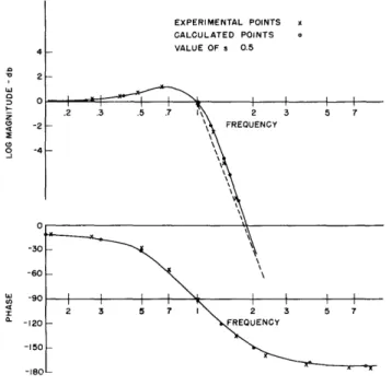
The experimental values for = 0. 5 are plotted in the graph of Fig. 18 along with the calculated values. 4 2 o C D -2 o -4 J -30 -60 u -90 -120 -150 -1RA EXPERIMENTAL POINTS x CALCULATED POINTS VALUE OF s 0.5 .2 .3 .5 .7 I 2 3 5 7 \ FREQUENCY
Fig. 18 The quadratic factor 1/s2 + 2 s + 1.
The agreement between the experimental and the calculated values is within 1 percent for the log-magnitude, and 3 percent for the phase. The experimental values were obtained from the negatives of the photographs by means of a projector-enlarger.
A Butterworth Filter
The prototype, low-pass Butterworth filter is represented by the transfer impedance Z12 in the formula
12
Z = IZn (42)
12 1 + s 2 n (
The zeros of this function are all at infinity, and the poles are distributed uniformly around the circumference of a unit circle in the s plane. For n = 4 the locations of the poles are shown on Fig. 19.
In order to realize the filter by a physical network, Z12 must be identified with the poles in the left half-plane. (This usage corresponds to the symmetry conditions about the j axis which were discussed earlier. ) The log-magnitude and the phase plots for this filter are shown in Fig. 20.
-29-I
"
i i I i 2 3 5 7 1\ 2 3 5 7 QREUENCY --U) I =~~~~~t I w~~~~~IV. . -4 N 4-N +j --4I a ) ., Q h ) u . 0 cd E r. V --U) 4 U -Q + 0N ) 3 _ . L b0 w a) 44H -4 '0 U ) U) 4-' ed = e0-4
~
r-_ , cC . o ; Y .H > F N S CC OC Ob bfl U) b.-bb cd 4~iI .r t E a, E (d -I V I 2 O ·- O o N N N ·r .~ .~ . M M bS bS o N b _-i .--30-0 r14 4-4 -QO-4 4 Cdcl C4-4 0 C-C U) -44 ) U)) C4 ,M d~~~~~-ci) U U) 0 ,-kc)0 N;a b. N N -31-___I