Displacement Sensors
by
SaiBun Wong
M.Eng., Electrical and Electronic Engineering
Imperial College of Science, Technology and Medicine (1995)
Submitted to the Department of Electrical Engineering and Computer
Science
in partial fulfillment of the requirements for the degree of
Master of Science
at the
MASSACHUSETTS INSTITUTE OF TECHNOLOGY
May 1998
©
Massachusetts Institute of Technology 1998. All rights reserved.
Author
... .
.-...
Department of Electrical Engineering and Computer Science
May, 1998
Certified by
...
David L. Trumper
Rockwell Associate Professor of Mechanical Engineering
Thesis ;Supervisor
Certified by
...
"Charles G. Sodini
Professor of Electrical E eer
g and Computer Science
Tu
u&exvisor
e~i
Accepted
by...
Arthur C. Smith
Chairman, Departmental Committee on Graduate Students
Displacement Sensors
by
SaiBun Wong
Submitted to the Department of Electrical Engineering and Computer Science on May 08, 1998, in partial fulfillment of the
requirements for the degree of Master of Science
Abstract
Capacitive displacement sensors are currently used in high-resolution non-contact displacement measurements such as wafer thickness and flatness. Currently these sensors are fabricated from discrete mechanical and electrical parts, with a triaxial cable connecting the sensor electrode at the mechanical sensor head to the sense elec-tronics on a printed circuit board. By having an integrated front end located in close proximity to the mechanical sensor, we expect to achieve nanometer-order resolution with a precise digital representation of displacement as the output, through elimina-tion of the triaxial cable. This is an improvement over the current sensors in terms of performance and cost. The main tasks of the thesis work are low-noise capacitance measurement circuitry design, high-resolution sigma-delta analog-to-digital converter design based on switched-capacitor techniques, and fabrication of a prototype of the design using a standard CMOS process.
Thesis Supervisor: David L. Trumper
Title: Rockwell Associate Professor of Mechanical Engineering Thesis Supervisor: Charles G. Sodini
I would first like to thank Professor David Trumper and Professor Charles Sodini who gave me the opportunity to work on this research. Their knowledge and guidance have provided me with a learning experience, both technically and (more importantly) otherwise, which I consider far more rewarding and important than anything I have learnt over the previous years.
This project would not be possible without the generous funding provided by the National Science Foundation and our industrial sponsor ADE Corporation.
Many people have also contributed technically and provided assistance throughout the course of this research. Many thanks to Professor Harry Lee for providing techni-cal guidance regarding the layout and circuit level design of the prototype chip when Charles was on sabbatical in Hong Kong. I would like to thank especially Michael Perrott, Don Hitko, Jeff Gealow, Iliana Fujimori, Ginger Wang, Dan McMahill, Pablo Acosta Serafini, Steven Decker, Jennifer Lloyd, Kush Gulati, Tracy Adams, Pradeep Subrahmanyan and Stephen Ludwick for their help in setting up my computer, get-ting me started with Cadence, and its associated technology files and various scripts, as well as providing me with helpful insights and advice on the prototype chip design and debug. Without their help I would not be able to make the fab deadline and to test the prototype chip. I would like to thank Maureen Lynch and Patricia Varley for handing the numerous administrative details of the research project.
In addition, I would like to thank Chao Wang for being my friend and also my study partner. Without her support and encouragements, I would not be able to survive the demanding course-works and the doctoral qualifying examinations. I also want to acknowledge my roommate Yu Sui for providing many helps, big and small, to make my life easier at MIT. I want to say a big 'thank you' to Lynn Wood who helped me out in various ways being my international student host under the Host for International Students Program of the International Student Office.
Kong Student Bible Study Group. With them I have spent some of my most enjoyable and memorial moments at MIT. I would especially like to thank Winnie Choi, Ernest Yeh, Oliver Yip, Ada Cheung and Jacky Ho for their support in prayers when I needed them most.
Finally I would like to thank my family members, in particular my parents and my brother whose support and encouragements are always there whenever I needed them. I would also like to thank God for being by my side always. I know I would not be able to be where I am now without Him.
SaiBun WONG May 1998
1 Introduction
1.1 Motivation ... .. ...
1.2 Objective ... .. ... 1.3 Highlights of the Project . . . .. 1.4 Thesis Organization ... .
2 Capacitive Displacement Sensing 2.1 Introduction ... ...
2.2 Currently Employed Sensing Schemes . . 2.2.1 The Resonance Method . . . . .
2.2.2 The Oscillation Method ... 2.2.3 The Charge-Discharge Method. . 2.2.4 The Transformer Coupled Charge 2.2.5 The Constant Current Method .
8 . . . . 8 . .10 . . . . . . . 11 . . . . . 12 14 . . . . . . . . . . .. . 14 . . . . . . . . . 16 . . . . . . . . . . . 17 . . . . 17 . . . . . 19 Pump Method . ... 20 . . . . . . . . . . 2 2 3 Sigma-Delta Analog-to-Digital Conversion 3.1 Introduction ... .... ... 3.2 Principles of Sigma-Delta Modulators . . . .. 3.3 Order and Noise-Shaping Function Selection . . . . 3.3.1 Design Constraints and Tradeoffs .. . ... 3.3.2 Obtaining Prototype Filter . . . .. 25 . . . . 25 .. . . . . 27 .. . . . . 32 .. . . . . 32 . . . . . 33
3.4 Coefficient Selection . . . . . . . . . .... 3.4.1 Derivation of Modulator Transfer Functions 3.4.2 Matching Coefficients and Approximations 3.4.3 Optimal Coefficient Selection . . . . 3.4.4 Numerical Verification . . . . . ..
4 Operational Amplifier Design
4.1 Introduction...
4.2 Folded Cascode Design . . . .. 4.3 Gain Enhancement ... .
4.4 Common Mode Feedback at Outputs . . 4.5 Common Mode Feedback at Inputs . . . 4.6 Choppers at Inputs and Outputs . . . .
4.7 Opamp Noise Considerations . . . .
5 Circuit Implementation
5.1 Capacitance-to-Voltage Conversion . . . 5.2 5th Order Modulator ...
5.2.1 Integrator . ... ... 5.2.2 Small Coefficients for Zeros . . . 5.2.3 Single-Bit Comparator . . . . 5.2.4 Distributed Differential Feedback 5.3 Layout . ... .... ... ...
5.3.1 Pin Assignment . . . .. 5.3.2 Opamps ... . ... 5.3.3 Capacitors ... ....
5.3.4 Electrostatic Discharge (ESD) Pr
45 . . . . . . . .. . 4 5 . . . . . . . . . . . . 46 . . . . . . 50 . . . . . . . . . . 53 . . . . . 56 . . . . . . . . . . 60 . . . . . . . . . . . 6 1 64 . . . . . . . . . . . 64 . . . . . 6 6 . . . . . . . . . 66 . . . . . . . . . . . . . . 6 7 . . . . . . . . . 69 . . . . . . . . . . 70 . . . . . . . .. . 72 . . . . . . . . . . . 72 . . . . 73 . . . . 73 tection . ... 74 .. 37 .. 37 .. 39 .. 42 .. 43 o1
6 Results
6.1 Simulation Results . . . . . . . . . ..
6.1.1 Capacitance-to-Voltage Conversion Circuitry . . . 6.1.2 5th Order Modulator ... ...
6.2 Measured Results . ... . . ... 6.2.1 Test Board Implementation . ...
6.2.2 Bit-Stream Capture Scheme . . . . . .. 6.2.3 Capacitance-to-Voltage Conversion Circuitry . . . 6.2.4 5th Order Modulator . ... ...
7 Conclusions
7.1 Conclusions ... ...
7.2 Suggestions for Future Directions . . . .. 7.2.1 Integration of C-V Circuit into Modulator Design
7.2.2 On-chip Constant Current Drive Circuitry . . ..
75 . . . . 75 . . . . 75 . . . . 77 . . . . 80 . . . . 80 . . . . 83 . . . . 84 . . . . . 86 92 . . . . . 92 . . . . . 93 . . . . . 94 . . . . . 96
Introduction
1.1
Motivation
The rapid evolution of the semiconductor industry, with emphasis on feature size re-duction to achieve high performance circuits, demands the development of high preci-sion displacement measurement systems for use in wafer steppers and mask aligners. Such systems are also used in wafer flatness and thickness measurements [1, 2, 3]. Ca-pacitive displacement measurement is frequently used for these measurements because of the inherent contact-less nature of the process. The currently available sensors are fabricated using discrete mechanical and electrical parts. Typically, electronics on a printed circuit board drive a triaxial probe through a triaxial cable. The triaxial electrodes on the probe are sense, guard and ground. The guard electrode is required both to null the cable capacitance and to improve the probe linearity by terminating fringe fields. Figure 1-1 [4] shows an example of such a capacitive displacement probe. A number of problems are associated with the current approach. First, the assem-bly process is challenging and expensive. The assemassem-bly of the probe triaxial structure must be accurate and be reliably connected to the triaxial cable with no sense/guard
sensor housing guard
insulator
triax
Figure 1-1: Typical capacitive displacement probe (Figure taken from [4])
leakage. The probe sense electrodes must then be precision finished by grinding and lapping to establish a smooth planar surface. Since the sensing electronics is sensitive to femtofarads of capacitance change, the cable must be of a special fabrication to avoid triboelectric charging effects which appear as noise when the cable is moved. The cable is then connected to the sense electronics using a triaxial connector, which is expensive and presents a reliability problem. In addition the cable is a strong source of electrical noise pickup, especially at 60Hz. Finally the fabrication cost is high even in volume production.
By going to an integrated solution, that is, by close integration of the sensor electrodes and the sense electronics, preferably on the same substrate, the above problems can be largely eliminated. A conversion circuit in close proximity to the sensor electrodes can then be used to obtain equivalent digital representations of the sensitive analog measurements. The assembly steps equivalent to those men-tioned above, in particular the triaxial cable assembly, probe, and connectors, will be eliminated, leading to lower cost, increased reliability, and increased resolution of capacitive displacement sensing. Such improvements can lead to a much wider range of applications for these sensors.
employed in the auto industry [5, 6, 7, 8, 9, 10] in which micromachining enables the construction of the sense element together with the electronics required for sensor readout on the same substrate. Similarly the integrated pressure sensor [11, 12] is yet another example. In these examples, sensors and actuators are placed in close proximity with signal processing circuitry leveraging existing integrated circuit man-ufacturing technology [13]. The most compelling reasons for such an approach is to improve the performance and to lower cost. Often the change in the physical param-eter, for instance the capacitance for an integrated acceleromparam-eter, is so tiny that it can easily be corrupted by noise introduced by the readout circuitry as well as that coupled via packaging, thus limiting the sensing system resolution. In addition, the increased use of digital signal processing systems dictates a digital sensor output. Consequently an integrated analog-to-digital conversion circuitry [5, 12] based on the sigma-delta approach is favored due to the high resolution, band-limited requirements for the conversion.
1.2
Objective
The objective of this thesis is to investigate the issues involved in the implementa-tion of an integrated capacitive displacement sensor that can satisfy the following specifications:
* digital output as a representation of displacement measured * displacement range: 100 pm ±50 pm
* resolution: 1 part in a million (approximately 20 bits)
The sensor presented in this thesis shows a promising implementation for an in-tegrated capacitive displacement sensor fabricated using a standard CMOS process.
For the displacement ranges we are considering, the most common sensor currently in use has an active circular sensing area with a diameter of 5 mm. The corresponding capacitance has a range of approximately 1.15 pF to 3.48 pF in air, over the typical measured range of 50 ,m to 150 ,m. With our target resolution being on the order of 0.1 nm, the change in capacitance to be measured is thus on the order of attofarads.
1.3
Highlights of the Project
Figure 1-2: Layout of our prototype chip
A prototype test chip was fabricated to demonstrate the feasibility of the integrated capacitive displacement sensor concept. Figure 1-2 shows the layout of the die. In
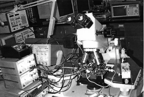
addition, an analog test board, as shown in figure 1-3, was custom designed for characterization and debug of our prototype chip. The test setup can be seen in figure 1-4. The design of our prototype chip and its associated testing is presented in the later chapters of this thesis.
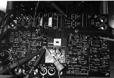
Figure 1-3: Analog test board with prototype chip
1.4
Thesis Organization
Chapter 2 gives an overview of the current implementation of capacitive displacement sensing. The different types of circuitry required to enable a readout of displacement are also presented in this chapter.
The underlying concept of sigma-delta analog-to-digital conversion is presented in Chapter 3. This conversion scheme allows us to achieve high resolution for a limited bandwidth without the use of precision on-chip analog components.
Chapter 4 describes the characteristics of the folded cascode opamp, bias circuit and switched capacitor common mode feedback scheme. This opamp forms the core of our switched-capacitor-based analog-to-digital conversion and is crucial for achieving
ii; iii!!::ii~i! i::iii::ii! : : ! ... : ; !.!i iiii ... ?. ... .. ... ....~~i~ : : .. I W. i .-" ... ::.:!- ..'~f
Figure 1-4: Test setup for prototype chip testing and debug
high performance.
The layout of the opamp is shown in chapter 5. Ideas for the incorporation of the capacitance-to-voltage conversion circuitry into the analog-to-digital conversion circuitry and their corresponding implementations are also presented.
Chapter 6 shows test results with our prototype chip. Chapter 7 concludes this thesis with suggestions for future work.
Capacitive Displacement Sensing
2.1
Introduction
Capacitive displacement measurement systems are currently employed in wafer flat-ness and thickflat-ness measurements [1, 2, 3], where no contact with the target, in this case the silicon wafer, is desired. In addition they also find applications in wafer stepper stages [14] being the fine position sensors for closed loop positioning.
Probe with Sense Area A Guards Displacement d Fixed " Grounded Target
These systems exploit the inverse relationship between the capacitance C and the distance d between the two conducting plates of an ideal parallel plate capacitor with overlapping area A in a medium whose relative permittivity is given by Er as shown in figure 2-1.
ErEOA
C=
d
There are three possible way to change the capacitance of a parallel plate capacitor:
* Variation of the permittivity Er of the dielectric between the plates [15, 16] * Variation of the distance d between the plates [17, 18]
* Variation of the area A of overlap between the plates [19, 20, 21, 22]
Here the interest lies in the variation of the distance d. However the same prin-ciples for capacitive sensing are also applicable generally to areas where either a capacitance or an inverse of capacitance has to be measured. The ideal relationship holds well for small values of d, provided that one of the plates has an area much larger than the other one, and the smaller plate has guard electrodes driven synchronously with the sensor plate.
Present systems can provide non-contact measurements, while delivering a high resolution, often measured by nanometers. The drawbacks include the constraint to a small displacement range, measured in terms of hundreds of microns, as well as an analog output. The increased use of digital signal processing systems dictates such an analog output be converted to its digital equivalent for data acquisition, storage and analysis. The main difficulty lies with the interface between the sensor and the high-resolution analog-to-digital converter. In the conversion process the sensitive
analog signal is likely to get compromised [14, 23]. It is envisioned that if the analog-to-digital conversion is performed as an integral part of the capacitive sensing process the sensor noise limits should be improved.
External Excitation
Analog Digital
Capacitance Capacitive Voltage Analog-to-Digital Output
C Displacement 0 Conversion
1Probe Circuitry
Displacement
d
Figure 2-2: Main blocks for capacitance displacement measurement
Hence in order to have a digital representation of the displacement to be measured, the current implementations involve two main components, namely the capacitive-to-voltage conversion circuitry and the analog-to-digital conversion circuitry, as shown in figure 2-2. It is desirable to achieve an integration of these two components for improved overall performance.
2.2
Currently Employed Sensing Schemes
The currently available sensors exploit the Q = CV principle. Here the capacitance
C is varied by the distance between the sensor electrode and the grounded target.
Numerous techniques exist for measuring small varying capacitances. However not all of them are realizable as an integrated circuit. In addition, a high performance system mandates a minimization of the effect of stray capacitances and a reduction in the baseline drift of the capacitance measurement circuits. A number of these techniques will be reviewed in the following sections.
2.2.1
The Resonance Method
C1
fr L Cx
Figure 2-3: Simplified circuit for resonance method
As shown in figure 2-3 [24], the voltage source outputs a sinusoidal signal to a voltage divider formed by a known capacitor C1 and a LC parallel circuit consisting of a
known inductance L and the unknown capacitance C. By adjusting the frequency fr of the sinusoidal signal, resonance can be found, and the unknown capacitance C can then be calculated:
(27fr)2L(Ci + C)= 1
The main limitation is the need to manually adjust the sinusoidal signal frequency until resonance occurs. This is not suitable for monitoring the continuously changing capacitance as in our intended application. In addition the difficulties in the realiza-tion of large inductances on an integrated circuit make the method less attractive.
2.2.2
The Oscillation Method
Yet another possibility is to incorporate the sensor capacitance into a network such that the oscillation frequency, or the time it takes to charge and discharge the sensor capacitance back to its original state, changes with the varying capacitance [11, 25, 26, 27, 28, 29, 30, 31, 32, 33]. The cycle time can then be measured using a simple synchronous counter. This is also known as the capacitance-to-frequency conversion
method.
o+( o Vout
Cx Schmitt Trigger
Figure 2-4: Circuit showing capacitance-to-frequency conversion
One possible implementation is shown in figure 2-4. Here C. is the unknown capacitor and I,+ and Io- are constant current sources. The output of the Schmitt trigger determines if C. is connected to the top or the bottom current source such that it is charged or discharged at a constant rate. As a result the voltage across C, rises or falls linearly with time. The output voltage Vout is a square wave whose period depends on the charging and discharging currents and C,. Ideally the oscillation frequency is:
Io
S2CxVh
where Vh is the hysteresis of the Schmitt trigger.
A further improvement is obtained by monitoring the supply currents to the Schmitt Trigger constructed from CMOS circuits, taking note that large currents flow only during transitions. From these current spikes then the oscillation frequency can be measured such that a 2-wire [25, 26] solution is possible.
The main advantage is the ability to be implemented as an integrated form with stray capacitances of lead wires are eliminated. However, this topology offers no
correction for any stray capacitances that appear in parallel to Cx. In addition, at least one complete cycle of charge-discharge is required. This sets a limit on the resolution and the bandwidth of the topology. Given a fixed clock rate for the counter, higher resolution calls for reduced charging and discharging currents and hence longer cycle time and lower resulting bandwidth. Finally the small changes in a relatively large capacitance makes it difficult to obtain high resolution due to the corresponding small changes in the oscillation frequency.
2.2.3
The Charge-Discharge Method
•I
ci Vout
Figure 2-5: Example Circuit for Charge/Discharge
Another possibility would be to charge the unknown capacitor C up to a known voltage Vref via a CMOS switch S1 and then discharge it into a charge detector via a second switch S2. This topology is essentially a switched-capacitor based
implemen-tation [15, 34, 35, 36].
As shown in figure 2-5, the charge transferred from Cx to the detector in a single charge/discharge cycle is Q = VC,. A detector can be implemented such that the charge Q is accumulated on an integrating capacitor Ci for multiple charge/discharge cycles before the voltage across Ci is measured.
A stray insensitive implementation is feasible if both terminals of the unknown capacitor C, is available. However we have access only to one terminal of our sense
capacitor.
Another switched-capacitor approach uses the charge-balancing concept [37, 38, 39]. In these implementations, the output of a DAC drives the reference capacitor such that the charge on it balances that on the sense capacitor on each charge/discharge cycle. When charge balance occurs, the DAC output is directly proportional to the capacitance C. to be measured.
One main advantage of this topology is the suitability for integrated circuit design as it is essentially switched-capacitor-based. One drawback is that any stray capaci-tance in parallel with C, is indistinguishable from C.. However, unlike the oscillation topology, the bandwidth is now constrained by the minimum time to charge/discharge C. fully rather than the cycle time of a synchronous counter.
2.2.4
The Transformer Coupled Charge Pump Method
Cprobe
V L - D2 _
lout
Figure 2-6: Transformer coupled charge pump circuitry
Figure 2-6 shows the transformer coupled charge pump circuit [40]. The inductance L represents the transformer inductance. The voltage source V is a high frequency
source with magnitude V. The drive frequency f, is much greater than so that the ac voltage developed across the probe capacitor Cprobe is essentially the same as the drive voltage, ignoring the diode drops. On each cycle, Cprobe is charged to V, through D1 and then discharged to -V, through D2. Thus an average current Iout
flows through resistor RF giving rise to an output voltage.
lout = VsfsCprobe D1 R C V D2probe V L D2 C2 Variable f Voltage Drive V
Figure 2-7: Improved transformer coupled charge pump circuitry
An improved version of the transformer coupled charge pump is shown in figure
2-7. By using a variable voltage drive V, the average current flowing out from Cprobe is
forced to assume the value Iref. Now the magnitude V, of the voltage drive V bears an inverse relationship to the capacitance Cprobe to be measured.
One main drawback of the design is the use of a transformer that cannot be readily realized as an integrated circuit. An transformer-less implementation [41] based on the charge pump idea is also feasible. However they both suffer from the use of diodes. Although diodes can be easily realized as part of an integrated circuit, the diode drops
are not negligible because the drive voltage is small due to technology limitations.
2.2.5
The Constant Current Method
The inherent advantage of measuring the inverse of capacitances is to have outputs that are directly proportional to the displacements of interest. The inversion is thus performed as an integral part of the design. To do so, one possibility is to transfer a fixed quantity of charge onto the sense capacitor such that the voltage developed is measured. Essentially the average current flowing through the sensor capacitor is kept constant, hence constant current method.
An example of such a design is shown in figure 2-8 [42]. In essence the target and the output of A2 are grounded. The capacitive displacement probe shown has the sense electrode, connected to the inverting input of A2 such that the capacitor formed by the sense electrode and the target is connected across the feedback path of
A2. The guard electrodes are connected to the non-inverting input of A2. The high
gain of A2 ensures that the guard electrodes are driven to the same potential as the sense electrodes.
Probe
_
TargetR
Vin + A 1
Assuming the stray and fringe capacitances is additive to the actual capacitance value measured, the variable resistor VR can be used such that the output voltage, if taken from the non-inverting input of A2, is directly proportional to the distance between the grounded target and the sense electrodes of the probe. With the as-sumption that the amplifiers are ideal, i.e. the positive and negative inputs have the same voltage due to feedback action and no current flows into the amplifier inputs, the following relationships can be derived:
VotA1 = 2V-A1 - Vin
Resistors R and VR essentially forms a voltage divider such that
R R
V+A1 R + VRV+A2 R +VR
From charge conservation,
0
oA
(VoutA1 - Vout)Cr = VoutCprobe = Vout
Thus the following relationship between the distance of interest and the output voltage results:
- VinCr
out = + Co - (2 - 1)Cr
where A is the area of the sense electrode, d is the displacement to be measured,
Co represents stray and fringe capacitances.
Hence an ac analog voltage Vout that bears a proportional relationship to the displacement d of interest can be obtained by adjusting the value of VR such that the term Co - (2R - 1)Cr is set to zero. Demodulation will then enables a dc
One main drawback of the design is that the power supplies of both opamps Al and A2 have to be referenced with respect to Vout taken from the non-inverting input of A2. In the current implementation this is achieved with the use of transformer which can not be readily realized as an integrated circuit.
Sigma-Delta Analog-to-Digital
Conversion
3.1
Introduction
The advent of VLSI digital IC technologies has made it attractive to perform many signal processing functions in the digital domain. Oversampled converters are becom-ing a dominant architecture for high-resolution and band-limited analog-to-digital conversion applications. This technique has been shown to provide high resolution without trimming or high precision components [43, 44, 45].
Anti-Aliasing Sigma-Delta Digital Decimator
Analog Filter Modulator and Filter PCM Output
Input
OverSampling Nyquist
Clock Fs Clock Fo
Figure 3-1: Block digram of a typical Sigma-Delta ADC
As shown in figure 3-1, the analog input signal, after passing through an anti-aliasing filter, is oversampled by the modulator at many times the Nyquist rate to produce a coarse quantization. The output is then decimated digitally to give the desired high resolution representation of the original input signal at the Nyquist rate. Quantization noise is effectively moved out of the signal band and can thus be removed by an appropriate digital filter with relative ease.
fb
fs
Nyguist Rate ADC
fb fs/2=fn fs-fb fs fs+fb
OverSampling ADC
Figure 3-2: Antialias filter requirements for Nyquist and oversample converters
One major advantage of an oversampled A/D system is the reduction in the com-plexity of the analog circuitry if the encoding is selected such that the modulator needs only to resolve a coarse quantization (usually a single bit). Also, if high over-sampling rates are used, the baseband will be a small portion of the over-sampling fre-quently. As shown in figure 3-2, with the baseband bandwidth being fb and the sampling frequency f,, the analog anti-aliasing filter has a transition band of f, - fb
in the Nyquist rate converter compared to fs - 2fb in the oversampling converter.
Clearly the more relaxed constraints permit a more gradual roll-off, linear phase and easy implementation. The precision filtering requirements is now relegated to the digital domain, where a 'brick-wall' anti-aliasing filter is required to low pass filter and decimate the digital output down to the Nyquist rate. Additional benefits can be gained with the digital processor which can also be used to provide other functions such as equalization, etc. A system that can provide integrated analog and digital functions and be compatible with digital VLSI technologies is feasible.
In our design, the oversampled sigma-delta modulator forms the core of our im-plementation that satisfies high-resolution (20-bits) and relatively low-bandwidth (1kHz baseband) requirements. The modulator order, together with a particular noise transfer function, is chosen to meet the analog-to-digital resolution require-ment. The implementation is switched-capacitor based and the design is performed in the discrete-time domain based on a linear system model [46, 47]. Simulation was then used for design verification and optimization of filter coefficients. Finally, the modulator was implemented by means of relative scaling of capacitor sizes on silicon. The capacitance-to-voltage conversion is also chosen to be a switched-capacitor based approach that eliminates the need for an anti-aliasing frontend filter.
3.2
Principles of Sigma-Delta Modulators
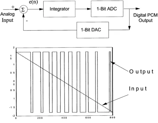
The simplest form of an oversampled interpolative modulator consists of an integrator, a 1-bit ADC and DAC, and a summer as shown in figure 3-3. The integrator has high gain at low frequencies. Feedback forces the output to lock onto a band-limited analog input. Unless the input exactly equals one of the discrete DAC levels, a tracking error
e(n) results. The integrator accumulates this error over time with the DAC output
levels such that its average is approximately equal to the average of the analog input. Digital PCM Output O utput Input 200 400 600 800
Figure 3-3: First order modulator and its time-domain waveform
The operation of the delta-sigma modulator is analyzed by modeling the integrator with its discrete-time equivalent and the quantization process as an additive noise source Q(z) as shown in figure 3-4. Q(z) is assumed to be a white noise source that is statistically uncorrelated with the input X(z) [43, 48]. Using this linearized model, it can be shown that
Y(z) = z-X(z) + (1 - z-')Q(z)
The overall closed-loop transfer function Y(z)/Q(z) for the quantization noise
Q(z) is a high-pass filter whereas that for the input signal Y(z)/X(z) is a pure delay.
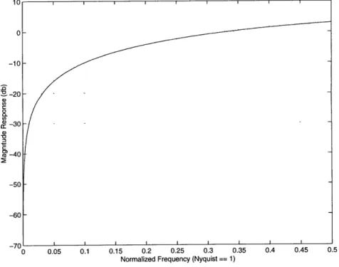
plot of the noise shaping function IY(ejw)/Q(ejw) = I1 - e-j I as shown in figure 3-5,
it is clear that by having the modulator sampling at much higher than the Nyquist rate, quantization noise in the base-band is greatly attenuated. Although a coarse quantization is made by the modulator, most of the quantization noise is pushed to higher frequencies which can then be removed by subsequent digital filtering. Once removed, the final output is a high-resolution digital representation of the input.
Q(z)
X(z) Z1 +
- 1 -Z + Y(z)
Integrator
Figure 3-4: Discrete time model of first order modulator
S-20 0 0. CL 0) CC -30 S-40 0 0.05 0.1 0.15 0.2 0.25 0.3 0.35 0.4 0.45 0.5 Normalized Frequency (Nyquist == 1)
The single-bit encoding scheme used has several advantages:
1. The format is compatible for serial data transmission and storage systems. This is important in our implementation since we want to minimize the number of connections between the sensing electronics and the sense electrodes [49]. 2. Subsequent digital signal processing operations are greatly simplified as
addi-tions and multiplicaaddi-tions are reduced to simple logic operaaddi-tions as these oper-ations can be reduced to simple bit-wise operoper-ations.
3. The inherent linearity of the in-loop 1-bit DAC guarantees highly linear con-verters. The integral nonlinearity of the in-loop DAC often limits the harmonic distortion performance of many oversampled A/D converter [50]. A multi-bit DAC has many discrete levels that must be precisely defined to prevent linear-ity error. With only two discrete values, a one-bit DAC always defines a linear transformation between the analog and digital domains [51]. This guarantees the linearity of the converter.
However many problems arise when implementing a sigma-delta A/D converter. The quantization noise is signal dependent [44, 52, 53] and not statistically uncor-related as assumed. This is uncor-related to the number of state variables in the system. For a sigma-delta modulator, the state of the system is determined by the integrator output value along with the input value. With only one state variable, the loop can lock itself into a mode where the output bit stream repeats itself in a pattern. As a result, the output spectrum can contain substantial peaks centered at multiples of the repetition frequency. To minimize this effect, dithering has been used to randomize the input to avoid the formation of repeating bit patterns. However such a technique lowers the input dynamic range.
(D/ g -40 -60 -80 / 1st Order -.-/ 3rd Order --100 -5th Order ----120 L 0 0.05 0.1 0.15 0.2 0.25 0.3 0.35 0.4 0.45 0.5 Normalized Frequency (Nyquist == 1)
Figure 3-6: Magnitude response for noise-shaping functions of the form (1 - e-j")N
loop, repeating bit patterns are less likely to occur, and, consequently, the quantiza-tion noise tends to become less signal dependent. In addiquantiza-tion, the higher order causes the quantization noise to be further attenuated in the low frequency baseband and to rise more sharply in the higher frequencies, with the net effect being a reduction in the total quantization noise power in the baseband, leading to a higher resolution for the same oversampling ratio. Figure 3-6 shows the magnitude responses of the
noise-shaping functions NS(ej") = (1 - e-j )N, for N=1, 3 and 5.
Our implementation is based on the single loop 5th order modulator. Single loop higher order modulators are conditionally stable systems, and no exact mathematical analyses exist for such nonlinear systems. In the following sections, the design issues about the order selection, stability analysis and simulation, modulator coefficient selection are presented.
3.3
Order and Noise-Shaping Function Selection
Here the emphasis is on the modulator resolution and bandwidth with power con-sumption and area being only secondary considerations. Consequently the ideal mod-ulator was designed to resolve better than 20-bit, to account for the inevitable res-olution loss once the capacitance measured is inverted to obtain the corresponding displacement values. The modulator design was chosen to give around 140dB signal-to-noise ratio over a baseband of 1kHz.
3.3.1
Design Constraints and Tradeoffs
The design was performed by starting with the noise-shaping function NS(z) of the modulator, assuming a linear additive quantization noise model, as NS(z) will de-termine the signal-to-noise ratio in the final output. The modulator coefficients can always be derived from NS(z) by algebra. These functions are all discrete-time func-tions such that it is well-suited for switch-capacitor based implementafunc-tions. In this phase brick-wall decimation filters, i.e. filters with zero transition region width, are assumed available.
There is as of yet no closed-form solution for the design of stable high-order loops. Instead, the design approach adopted by R. Adams [43, 44, 54] is to ensure that
NS(z) exhibit the following properties: 1. NS(z) is a high-pass filter.
2. The high frequency gain of NS(z) is about 1.4.
3. The first value of the impulse response of NS(z) is unity.
The first requirement is a direct result from the need to move the quantization noise out of the low-frequency baseband. The second one comes from the fact that
high frequency gain of NS(z) determines the low-frequency comparator input am-plitude, which in turn determines the low-frequency comparator gain as seen by the loop. According to R. Adams [43, 44, 54], such a requirement usually yields a stable first-cut NS(z) whose coefficients are then further adjusted. The loop filter of the modulator has at least one sample delay, as a delay-free loop cannot be easily imple-mented in the actual switched-capacitor based circuit. Assuming a linear quantizer model, the quantization noise input will then immediately appear at the modulator output. Hence the third requirement results.
The oversampling ratio was chosen to be 512 such that the master clock for the modulator is about 1MHz for a baseband of 1kHz. These were chosen such that the modulator is clocked at a rate that allows full settling of the opamps that make up the design implementation.
NS(z) was chosen to be a 5th order filter. A 4th order NS(z) can just meet the
noise shaping requirements. However, the use of a 5th order design allows extra room to account for contributions from other noise sources such as the input referred noise of the amplifiers. In addition, a 5th order design allows using 2 complex zero pairs, producing nulls for quantization noise in the signal passband of the modulator. This leads to further improvements in the signal-to-noise ratio by lowering the quantization noise over a wider range of frequencies compared with a design that places the zeros at DC. As a result, the prototype filter for NS(z) is a 5th order inverse Chebychev filter.
3.3.2
Obtaining Prototype Filter
Using MATLAB, a 5th order inverse Chebychev filter was designed to satisfy the requirements outlined in section 3.3.1. The cutoff frequency w~ and the stopband attenuation Rs were the two variable design parameters. An iterative approach was
-50-100 -1501-101 Figure 3-7: 102 103 Frequency
Ideal Inverse Chebychev
104 10
s
106
Noise-Shaping Response
taken to determine optimal w,, and Rs. Figure 3-7 shows the frequency response of the resulting NS(z) with w, = 0.002 and R, = 180.6 which meets the design requirements to give an approximate total attenuation of 142.5db for the 1kHz baseband. This translates to approximately 23 bits [55] under ideal conditions.
The zero pairs of the inverse Chebychev filter have frequencies very close to DC such that they are not obvious in the pole-zero plot of figure 3-9. However the nulls they introduced can be easily seen in figure 3-8 which shows the low frequency region of the frequency response.
The resulting NS(z) exhibit the following form:
1 + al1z 1+j a2Z2 + 3Z - 3+ z4 z - 4 05 - 5 Iv Sz) = 1 + 01Z - 1 + 02 Z-2 t /03 z-3 + / 4 Z-4 + / 5 Z-5 with r.n fin I' . .- . ~ 13 I . . . .
-140 -160 S-180 'a ~-200 -220 -240 -260 ' . . . .. 10- 1 100 103 110 Frequency (Hz) 1_40 200 400 600 800 Frequency (Hz) 1000 1200 1400
Figure 3-8: Baseband of Ideal Inverse Chebychev Noise-Shaping Response
al1 2 a3 a4 a5
-4.2567630520 7.2958465820 -6.2888002393 2.7245733959 -0.4744049808
01 /2 03 /4 /5
-4.9999506520 9.9998519565 -9.9998519565 4.9999506520 -1.0000000000
The incorporation of noise-shaping zeros at frequencies other than DC shifts the O's slightly. A better appreciation of their presence is the zero and pole locations given below: Poles: pl = 0.9096625695 + 0.2024658718i p2 = 0.9096625695 - 0.2024658718i p3 = 0.8221883699 + 0.1130974371i -160 m -180 S-200 -220 -240 -260 0 I I ' ' I
0.5 - "
-0.51--1 -0.5 0 0.5 1
Real part
Figure 3-9: Ideal Inverse Chebychev Filter Pole-Zero Plot
p4 = 0.8221883699- 0.1130974371i p5 = 0.7930611733 Zeros: - 0.9999827148 + 0.0059756367i - 0.9999827148 - 0.0059756367i - 1.0000018418 - 0.9999916903 + 0.0036931540i - 0.9999916903 - 0.0036931540i x x • .x ... O ... I .. .. .. .. . .. . . .
3.4
Coefficient Selection
3.4.1
Derivation of Modulator Transfer Functions
Once the desired noise shaping function is selected, the next step is to determine the coefficients of the linear discrete time modulator model as shown in figure 3-10, i.e. the b's, c's and y's. The implementation is based on a cascade of 5 integrators with distributed feedback. Two local resonators implement the noise-shaping zero pairs at frequencies other than DC. The distributed feedback nature of the quantized feedback signal in such a realization enhances the stability characteristics even under conditions when one or more of the integrators are in saturation [51].
Vin cl z- ei - c2z-1 e2 cz e3i- _ c4z-1 e4 c5z-' e5 Vout
+ 1-z1 + 1 -Z- +1-+' + _ -z1 + _
1-z-bl=1 b2 b3 b4 b5
Figure 3-10: Discrete-time model for 5th order modulator
Using a linear model for the quantizer, we can replace the quantizer by a model where the relationship Vt = Q + e5 holds [43, 48]. The following equations can then
be derived: C1 -1 el (= (Vin - bl Vout) 1 - z-1 c2z-1 e2 = 1 - -C 1 (el - b2Vout - 73e3) 1- z-1 C3Z - 1 e3= - - 1(e2 - b3 Vout) 1 - z-( c4 z-1 e4 1 - - 1(e3 - b4Vout - 7y5e5)
C5Z - 1 e5 = 1
(
e4 - b5Vout)
1 - z-1
With these relationships the signal transfer function ocan be found as shown below. It is essentially a low-pass filter function such that signals falling within the baseband can get through the modulator unattenuated.
Vout(z) c1C2C3C4C5z - 5 Vin(Z) D(z) where D(z) {(1 - z-1)5 + yc2C3 -(1 - z-1)3 + -5C4c5-§(1- z-1)3 +y35c2C3C4C5z-4(1 - z- 1) + b3C3C4 5 -3(1 - z-1) 2 +b2C2c3C4C5- 4(1 - z- 1) + blC1C2C3C4C5Z- 5 +b4C4C5 -2(1- z-1)3 + Y3C2C3b4c4c5z-4( - z- 1) +c5b5z-1(1 - z-1)4 + 73C2C3C5b5z-3(1 - z-1)21
Similarly, the noise transfer function Vou Q can be derived. Essentially it is a high-pass filter with large attenuation in the baseband of interest. The width of the baseband, the magnitude of the attenuation and the transition characteristics are the design parameters.
Vout
(z)
N (z)
Q(z)
D(z)
where
+ Y375C2C3C4C5 z-4(1 - z- 1)
Both the noise transfer function and the signal transfer function have the same denominator D(z), a direct consequence of the linear model assumption with Vi, and
Q being the inputs to the loop. N(z) has 4 zeros that are not at z = 1 due to
the resonators implemented by 73 and y5 which shift them from DC towards higher
frequencies to achieve a improved noise attenuation in the baseband of interest.
3.4.2
Matching Coefficients and Approximations
The more difficult step is to map the coefficients of NS(z) to the ones of the actual modulator implementation comprised of b's, c's and y's. By choosing the appropri-ate values for b's, c's and y's, the swings at the intermediappropri-ate nodes, namely el to
e5, will be within the limits defined by the maximum swings of the opamps. The
smallest capacitor that can be realized is limited by the parasitic capacitance while the largest capacitor by the area consumption. As a result, the capacitor spread, i.e. the coefficient ratios, has to be minimized.
Here, it becomes a problem of choosing 12 unknowns with only 9 equations. The approach is first to make some approximations to simplify the set of equations and then select certain key modulator coefficients and finally solve algebraically for the rest. Difference equation simulations, using MATLAB and a customized simulator written in C by J. Lloyd [12] extended as part of this thesis project to accommodate resonators used for zero implementation, were used to determine if the constraints on opamp swings and capacitor spreads were met. The procedure involved some trial and error because the problem itself was underconstrained. There can be more than one set of modulator coefficients that implement the same noise transfer func-tion. However only a few sets are feasible due to opamp swings and capacitor spread
limitations.
The 9 equations below relates the modulator coefficients to the numerator and the denominator coefficients for the noise transfer function NS(z):
a2 = 10 + 73c2C3 + 7y5C4C5 a3 = -10 - 3-73c2 3 - 37Y5c4c5 O4 5 + 373C2C3 + 37 5C4C5 7375C2C3C4C5 a5 = -1 - 73C2C3 - Y5C4C5 - 7375C2C3C4C5 01 = -5 + cb 5 02 = 10 + ' 3C2C3 + 75C4C5 + b4c4c5 - 4c5b5 /33 = -10 - 373C2C3 - 375C4C5 + b3c3c4C5 - 3b4C4C5 + 6b5c5 + ' 3C2C3C5b5 04
=
5 + 73c2C3 + 3,y5c4c5 + 7375c2C3c4c5 - 2b3C3c4c5 + b2c2C3c4c5 + 3b4c4c5 +73C2C3C4c5b4 - 4c5b5 - 2y73C2C3c5b5 5 = -1 - 73C2C3 - '75C4C5 - 7375C2C3C4C5 + b3c3c4c5 - b2C2C3C4c5 + blC1C2C3C4C5 -b 4C4C5 - 73C2C3C4C5b4 + C5b5 + 73C2C3 5b5where the a's are the coefficients of the numerator and the 3's are the coefficients of the denominator of the noise transfer function. These were determined as described previously.
The first step to approach the problem is to identify which modulator coefficients can be determined first. From figure 3-10 it can be seen that the choice of c5 probably
does not matter because it is a gain term in front of the non-linear quantization block. Assuming the single-bit quantizer is ideal, changing c5 does not change the quantizer
output. Also, bl is chosen to be unity because it is desirable to have Vt following Vin. Considering the modulator as a feedback loop, the path where bl locates is essentially
a negative feedback path such that by setting the gain, i.e. bl, to be unity, the error
el is minimized and Vout tracks Vi,.
From the a's, it can be seen that they contain only the following combination of modulator coefficients, namely c2C3'y3 and c4C575 such that the zeros of the noise
transfer function are the solutions of the following equations in the z-domain:
(-l+z) = 0
(1 - 2z + z2 + C2C33) = 0 (1 - 2z
+
z2 + C4C575) = 0By solving for the zero locations, c2C3y3 and c4C575 can be determined. They
were found to be on the order of 10-5. An approximation was then made regarding the denominator coefficients i.e. O's. The terms that involve C2C3Y3 and c4cC55 were
ignored. This simplified the f-related equations greatly as they are now free of 73
and 75. Now the denominator coefficients are essentially the same as those of the modulator that does not have resonators which give rise to the y's.
The simplified equations relating the modulator coefficients to the denominator coefficients of the noise-shaping function NS(z) are as follows:
01 = -5+ c5b5
02 = 10 + b4c4C5 - 4c5b5
f3
= -10 + b3C3C4c5 - 3b4C4C5 + 6b5c5f4
=
5
- 2b3c3c4C5+
b2C2C3C4c5+ 3b4c4c53.4.3
Optimal Coefficient Selection
The coefficient selection process is a trial-and-error process. With the approxima-tions and preliminary selecapproxima-tions made in section 3.4.2, the problem is now reduced to choosing 9 unknowns with 9 equations. However, the difficulty now is that the unknown coefficients are not linearly independent of each other. It seems that these
coefficients form pairs such that c5b5 has to be determined first, followed by C4b4, C3b3,
c2b2 and finally c1bl.
The approach is to provide initial guesses of cl, bl, c3, c4 and c5 such that
corre-sponding b2, C2, b3, b4 and b5 can be derived. Difference equation simulations were
then used to check the swings at individual integrator outputs and conditional sta-bility. Simulations were also used to determine how the capacitor spread and the integrator swings are affected by the initial guesses. Based on the trends observed, if any one of the integrator swings becomes too large, another informed guess of the modulator coefficients will be made and the simulation re-run. After some number of iterations, the following modulator coefficients were found:
Coefficient bl b2 b3 b4 b5 Value 1.0000000 0.6246587 0.4869796 0.4838783 0.2972948 Stable Range ±5% ±17% ±14.4% +8.3% ±23.5% Coefficient Cl c2 c3 C4 C5 Value 0.0378000 0.1000000 0.2150000 0.2222000 1.0000000 Stable Range ±74% ±15% ±9.7% ±22.5% ±98% Coefficient 73 75 Value 0.0006344 0.0000643 Stable Range ±10x ±10x
device-level implementation will be covered in section 5.2.
3.4.4
Numerical Verification
Numerical simulation were used extensively for guiding the modulator design and ver-ification. On the system level, a MATLAB program and the simulator from J. Lloyd were used to independently to numerically verify the implementation and their re-sults cross-checked. For a given sinusoidal input signal, the corresponding modulator spectrum was calculated and the modulator stability verified.
One level down for the implementation is the switched-capacitor based simulation. SWITCAP2 was used for the task. In essence, after the optimal modulator coefficients are determined, they are implemented as capacitor ratios as described in section 5.2. SWITCAP2 then take these capacitor ratios and simulate the whole modulator using ideal switches and amplifiers giving rise to simulation results that are checked against those from numerical simulations.
Figure 3-11 shows a spectrum for the modulator output, using a differential si-nusoidal signal of 1kHz at 1.6V peak-to-peak. Numerical accuracy of the simulation makes calculating the signal-to-noise ratio for the implementation difficult. On the other hand, the high frequency noise shaping characteristics match those predicted by numerical simulations and the original prototype filter. This gave a good indication of the correctness of the switched-capacitor implementation.
-20 -401 ) 60 --80 -100 -120 -140--1601 10 Frequency (Hz)
Figure 3-11: SWITCAP2 simulated modulator spectrum
w i r I II Ali ~ ; 1 10
Operational Amplifier Design
4.1
Introduction
As our implementation is a switched-capacitor based, the most important component is the operational amplifiers (opamps) which form the heart of the design. Two fully-differential designs are used. The only major difference is the implementation of common mode feedback, which is required to ensure the opamp outputs are not saturated.
The performance requirements of the opamps are determined by those of the delta-sigma modulator itself. As the modulator is switched-capacitor based, each individual amplifier has to settle to the desired 20-bit target resolutions of the modulator within half of the period of the clock driving the MOS switches. This means the total settling time is approximately 14 time constants. As the designed clock rate is 1.024MHz, the total settling time is assumed to be half of the period of q2 plus 20% margin of
error. This translates into a time constant T of:
If the feedback ratio around the amplifier is 3, the relationship between the time constant 7 and the unity gain bandwidth
f,
can be shown to be:1
T
Assuming a minimum feedback ratio
3
of -, we will require the amplifier to exhibit a unity-gain bandwidth of approximately 143 MHz in order to meet the 20-bit settling requirement.The following sections will discuss the fundamentals of the opamp designs, the two different common mode feedback schemes and the reasons behind their usage, and the sizing and biasing of the transistors for gain, settling and noise considerations.
4.2
Folded Cascode Design
Because of the fabrication process chosen, the intrinsic output resistance of the tran-sistors are limited. Cascoding is thus used to boost the overall output resistance.
Here a folded-cascode design, essentially a single stage topology, is chosen. An im-portant feature is that the settling behavior is dominated by a single-pole resulting from the amplifier output resistance and the load capacitance. A high phase margin is achievable if only this pole affects the frequency response at crossover. The second pole of this topology arises from the gate and drain capacitances seen at the drains of transistors M1, M2, M3 and M4. This second pole prevents a full 90 degrees phase margin to be achieved.
In figure 4-1, PMOS transistors M1 and M2 form the input differential pair. The use of PMOS input transistors enables NMOS transistors to be used as M3 and M4. These two transistors carry the largest current and thus have the largest sizes. Being NMOS they can be made approximately 3 times smaller than if they are
Vdd lb2a lb2b 0- --_0 0 0n+ Vout- Vb2 Vout+ Vin+ n-M5 M6 Vb1 M3 M4 Vss
Figure 4-1: Folded cascode opamp design
PMOS, leading to a corresponding smaller capacitance at their drains. Consequently the second pole of the amplifier is high in frequency that the single dominant pole assumption of the design is valid. Transistors M5 and M6 are the folded cascode transistors. Voltages Vbl and Vb2 are fixed bias voltages. The small signal differential voltage gain can be derived by considering only the half-circuit (M1, M3 and M5) as the design is symmetrical.
Figure 4-2 shows the simplified half-circuit schematic used to derive the differential gain. Here the bias current source Ib2a is assumed to be ideal and have finite output resistance Rop, which can be derived later from the actual circuit implementation. The source of transistor M1 is assumed to be at analog ground for fully differential small-signal input voltages. Hence the output resistance associated with the bias current source Ibl can be safely ignored in the analysis. Being fixed bias voltages,
Rop
Vin
oL
M5
- M3
Figure 4-2: Half circuit of folded cascode opamp
Vbl and Vb2 at the gates of M3 and M5 respectively are assumed to be at analog
ground for small-signal analysis.
From figure 4-3, the following current-voltage relationships can be derived:
Vo + Vgs 5 Vs5
gmsVgs5 + r 7 = gmVi
ro7
T1//rI
T
The small signal differential voltage gain is thus given by:
Vo
Gain
=-Vi
mi(rop((1 o/ro )( l 3 + m5ro5) + o5)
((ro1//o)(1 3 + gm5ro5) + ro) ± Rop5
To maintain a high overall amplifier output resistance, the current sources Ib2a and 1b2b are implemented as cascode current mirrors. Their output resistances can be derived using the simplified small signal model as shown in figure 4-4.
ro3 0 Vgs5 Vout Rop
ro5
gm5 Vgs5 gmlVgslFigure 4-3: Small signal half circuit of folded cascode opamp
Ro9
Vgs7
Figure 4-4: Small signal model of cascode current mirror
Another important design criteria is the frequency response. The dominant poles of the amplifier are the ones due to the output load capacitor CL and the parasitic capacitance CL2 seen at the node where the drains of transistors M1 and M3 join with the source of transistor M5.
The first dominant pole for small differential signals is at: 1
pl 27r(Ron//Rop)CL
Vin=Vgsl
O-where
Ron = (1 + gm5ro5)(ol//ro3) + ro5
The resistance seen at the node where CL2 is located can be found using open circuit time constant analysis:
(rol//ro3)r o5
RL2
ro5 + (rol / /ro3)(1 gm5o5)
Hence the second dominant pole for small differential signals is at:
To5 + (rol//To 3)(1 + gm5ro5) 9m5
2 = CL2(o 1//ro3)ro5 2FCL2
4.3
Gain Enhancement
To improve the overall gain of the amplifier a feasible way is to boost the output resis-tance. One possibility would be adding yet another cascode transistor. However the associated further reduction of output swing [56] is undesirable. Another possibility is to use devices with a wider gate lengths which raises the intrinsic output resistances. Unfortunately the high bias currents required for the settling requirement dictates a high penalty in terms of chip area. As a result, the gain enhancement topology, as shown in figure 4-5 is employed.
Without the amplifier A the output resistance seen at the drain of transistor M2 is of the order gm2rolro2, ignoring that of the biasing current mirror Ibias, with the gate of transistor M2 being held at small-signal ground. With the amplifier A in place, the output resistance is raised by a factor equals to the gain of the amplifier to Ag,2rolro2. The amplifier A provides extra isolation of the drain of transistor M1 from the output node and hence enhances the overall output resistance.
Vdd
Q
Ibias Vout M2 Vin o0 M1 VssFigure 4-5: Circuit illustrating simple gain enhancement
A shown in figure 4-5. The advantage of the approach, as shown in figure 4-6, is the
simplicity of the implementation. However, the gain enhancement is limited to just a fraction of a single gr.
The gain resulting from MG1 and current source Ibg is gmG1(roG1//rolbg). In reality Ibg is implemented using a single transistor. Its output resistance is thus the transistor's intrinsic output resistance. Here the bias current of MG1 is small com-pared to that of the main amplifier. The transistors making up this gain enhancement topology have long gate lengths to boost their intrinsic output resistances raising the overall output resistance of the active cascode of the order g r3
By using a similar approach it is possible to design an amplifier which has an differential small signal gain which has the order gr 3 A simplified circuit schematic is shown in figure 4-7. The devices MG1, MG3, MG6 and MG8 are the single transistors that implement the gain enhancement. These transistors, as they are not driving the output capacitance directly, can be biased with smaller bias currents and