Air Trenches for Dense Silica Integrated Optics
by
Milos Popovid
Submitted to the Department of Electrical Engineering and Computer Science
in partial fulfillment of the requirements for the degree of
Master of Science in Electrical Engineering
at the
MASSACHUSETTS INSTITUTE OF TECHNOLOGY
February 2002
@
Massachusetts Institute of Technology 2002. All rights reserved.
Author...
Department/of Electrical Engineering and Computer Science
February 4, 2001
Certified
by...
Hermann A. Haus
Institute Professor Emeritus
Thesis Supervisor
Accepted by...
-Arthur C. Smith
Chairman, Department Committee on Graduate Students
MASSACHUSTh 11; OF TECHNOLOGY
A
PHR...
1
720TTE2
LIB
MITLibraries
Document Services
Room 14-0551 77 Massachusetts Avenue Cambridge, MA 02139 Ph: 617.253.2800 Email: [email protected] http://libraries.mit.edu/docsDISCLAIMER OF QUALITY
Due to the condition of the original material, there are unavoidable
flaws in this reproduction. We have made every effort possible to
provide you with the best copy available. If you are dissatisfied with
this product and find it unusable, please contact Document Services as
soon as possible.
Thank you.
The images contained in this document are of
the best quality available.
* Archives copy contains grayscale images only. This is the
Air Trenches for Dense Silica Integrated Optics
by
Milo§ Popovid
Submitted to the Department of Electrical Engineering and Computer Science on February 4, 2001, in partial fulfillment of the
requirements for the degree of Master of Science in Electrical Engineering
Abstract
Air trench structures for reduced-size bends in low index contrast (e.g. silica) waveguides are proposed. The proposed air trench bends (ATBs) improve on previous structures employing trenches for sharp bending by the introduction of a new "cladding taper" which eliminates junction loss between the low index contrast and air trench regions, and allows a smaller radius (5-15pm) limited by bending loss to be used. This bend geometry is general in the size-for-loss tradeoff, and offers an effective bend radius reduction dictated by the newly
introduced low index material in the trench; a reduction by a factor of 30-60 in effective radius is predicted for silica integrated optics (20-250p-m in size). Design considerations for bends and cladding tapers are presented. Bending, junction and substrate losses are investigated. 2D FDTD/EIM simulations of complete ATBs in representative silica index contrasts are presented. For proper account of substrate loss in the third dimension, an air trench waveguide cross-sectional geometry is investigated that allows for arbitrarily low substrate loss to be achieved at the expense of a deeper trench. The required trench depth, for an acceptable substrate loss, is calculated. A simple, compact waveguide T-splitter using ATBs is presented.
Thesis Supervisor: Hermann A. Haus Title: Institute Professor Emeritus
Acknowledgments
I would like to thank Profs. H.A. Haus and E.P. Ippen for their mentorship over the course of this thesis work, and all of my colleagues for making it a continuing thrill and challenge to work in their midst.
In the context of the work presented in this thesis, I owe a debt of gratitude to my collab-orators on the air trench bend project, Shoji Akiyama, Dr. Jirgen Michel and particularly
Dr. Kazumi Wada, whose suggestions initiated the project.
I am also grateful to my (former and current) officemates Christina Manolatou and M. Jalal Khan, who were happy to bring me up to speed when I began my graduate research. Christina's well-written FDTD simulation code, used throughout this thesis, has saved me countless hours of programming and allowed me to concentrate on the project. Jalal and I have spent hours debating all from waveguiding to world politics, sometimes in an amusing combination but always worth the time. I would like to thank all of my other colleagues (current and former) in the optics group for their part in introducing me to this or their research when I first joined this research group, and for offering their advice when needed. This includes Mike Watts, Dan Ripin, John Fini, Matt Grein, Leaf Jiang, Juliet Gopinath, Pat Chou, Hanfei Shen, Jason Sickler, Laura Tiefenbruck, Pete Rakich, Aaron Aguirre, Charles Yu and Poh-Boon Phua. I would also like to thank Tom Murphy for kindly offering his advice to me, and for letting me use some of his code for dual boundary bends. I have my sister and parents to thank for helping me get this far, and my wife Katherine for patiently putting up with my late hours over the past two months of writing this thesis. It's lucky this thesis is finished before her birthday.
Finally, I am very grateful for the support of an MIT Presidential Fellowship, a National Science and Engineering Research Council (NSERC) of Canada Scholarship, and our grant on the NPACI Cray T-90 supercomputer at SDSC for all FDTD simulations in this thesis.
Dedicated to my super grandparents in Yugoslavia, Kosara and Tomislav Jelenkovi6, and Miroslava Risti.
Posvedeno mojim bakama i deki u Jugoslaviji, Kosari i Tomislavu Jelenkovi, i Miroslavi Risti6.
9
Contents
1 Introduction: Integration of Optical Devices in Silica 15
1.1 Silica in Integrated Optics [42],[28] . . . . 16
1.2 Previous Work on Dense Integration, Sharp Bends and Air Trenches . . . . 18
2 Analytic Tools for Planar Waveguide Structures 21 2.1 Modal Expansion of Fields . . . . 22
2.2 Mode Solvers and FDTD . . . . 25
2.2.1 Electromagnetic Theory on a Lattice [9],[74] . . . . 25
2.2.2 Finite-Difference Time-Domain (FDTD) [74],[63] . . . . 27
2.2.3 Vectorial 2D Cross-section Waveguide Mode Solver [51] . . . . 28
2.3 Effective Index Method [22],[65] . . . . 31
2.3.1 Standard Effective Index Method [22] . . . . 31
2.3.2 Perturbation-corrected Effective Index Method [11] . . . . 32
2.4 Junction Loss at Waveguide Interfaces [65],[47],[5] . . . . 34
2.4.1 Junction Scattering via Mode Expansion and Transfer Matrices . . . 35
2.4.2 Straight-Straight Waveguide Junction Loss . . . . 37
2.4.3 Straight-Bent Waveguide Junction Loss [47] . . . . 38
2.5 Bend Loss in Step-Index Slab Waveguides . . . . 40
2.5.1 Analytic Methods for Single and Dual Boundary Bends [47],[18],[16],[53] 41 2.5.2 Qualitative Dependencies of Bend Loss and the Leaky Mode Field . 47 2.5.3 Optimal Design of Bends Terminating in Straight Waveguides . . . . 52
2.5.4 Optimal (Non-circular) Terminating Bend Geometry . . . . 56
2.6 Substrate Loss in Straight Leaky Waveguides . . . . 58
CONTENTS
2.6.2 Substrate Loss of 2D Cross-section Waveguides by the Equivalent
Source Method ... ... 67
3 Air Trench Bends: Design and Simulations 73 3.1 Limiting Factors of Integration Density in Silica . . . . 74
3.1.1 Index Contrast and Bend Loss in Integration Density . . . . 74
3.1.2 Scattering Loss and Fiber-to-Chip Coupling Limitations ... 78
3.2 Silica Waveguides and Optical Circuit Layout . . . . 79
3.3 Air Trench Waveguides . . . . 81
3.3.1 Cross-sectional Geometry for Strong Lateral Mode Confinement . . 81
3.3.2 Bends in Air Trench Waveguides . . . . 85
3.3.3 The Cladding Taper: A Low-Loss Interface to the Silica Waveguide. 92 3.4 Air Trench Bends for Silica PLCs . . . . 101
3.4.1 ATB Geometry . . . . 102
3.4.2 Numerical Simulation of ATBs . . . . 103
3.4.3 Loss Mechanisms: Substrate and Scattering Loss . . . . 114
3.4.4 Fabrication . . . . 115
4 Beyond Air Trench Bends 121 4.1 Waveguide T-splitter using Two Air Trench Bends . . . . 121
4.2 Concluding Remarks . . . . 122
4.2.1 Future Directions . . . . 124
A Reflection of Complex Waves at a Planar Boundary
10
11
List of Figures
1-1 Integrated optical components for which bend radius is an important parameter 17 1-2 Techniques for low-loss sharp bends on low and high index contrast platforms 19
2-1 Grid/field definitions for a discrete electromagnetic theory on a lattice (FDTD) 27 2-2 Electric field distribution of air trench waveguide quasi-TE and quasi-TM
fundamental modes . . . . 30 2-3 Effective Index Method for buried, rib and air trench waveguides . . . . 31 2-4 Field distributions comparison from (2D) Effective Index Method and (3D)
vectorial mode solver . . . . 33 2-5 Scattering at a junction: dielectric stacks; straight and bent slab interfaces 34 2-6 Single and dual boundary waveguide bend geometry and the radiation caustic 40 2-7 Index profile of a bend and the equivalent straight waveguide (conformal
m apping) . . . . 42
2-8 WKB and Airy function field distribution solutions for leaky mode of bend 45
2-9 FDTD simulations of single and dual boundary air-clad bends . . . . 49 2-10 Leaky modes of single and dual boundary silica bends . . . . 51 2-11 Single boundary bend loss vs. index contrast and radius . . . . 53 2-12 Generic dual boundary bend dimensions; illustrated total loss optimization 54
2-13 Schematic of optimal bend geometry progression over a range of loss values 55
2-14 Leaky mode diagram of a layered ID waveguide . . . . 60 2-15 Substrate loss of layered (ID) leaky waveguide . . . . 63 2-16 Equivalent current sheet configuration for layered 1D waveguide . . . . 64 2-17 Equivalent current sheet configuration for air trench (2D) waveguide . . . . 68 2-18 Substrate loss results for straight, truncated air trench (2D) leaky waveguide 72
3-1 Crosstalk and bend loss effect on integration density: example circuit layout 76 3-2 Waveguide crosstalk and bend loss bounds on integration density . . . . 77 3-3 Polarization-independent integrated optical circuit topology . . . . 81 3-4 Air trench waveguide cross-sectional geometry . . . . 82 3-5 Air trench waveguide mode (dominant E-field component) contour plots for
exam ples A-C . . . . 84 3-6 Idealized (infinite) and actual (finite-depth) air trench waveguide . . . . 85 3-7 Bend loss and whispering gallery mode width in the air trench waveguide 87 3-8 Straight ATW-straight silica waveguide junction loss vs. index contrast . 89
3-9 FDTD simulations of dual boundary, finite-angle ATW bends . . . . 92
3-10 Conventional tapers and the problem of interfacing ATWs to silica waveguides 93
3-11 Cladding taper geometries . . . . 94
3-12 Ray-optical estimate of required cladding taper angle for low loss . . . . 97
3-13 Guided power confinement of fundamental TE mode in slab waveguide . . . 99
3-14 Search algorithm for finding the optimal cladding taper, and example data. 100 3-15 FDTD electric field amplitude plots of cladding taper designs for case study
exam ples A-C . . . . 101
3-16 Schematic of Air Trench Bend geometry and free parameters . . . . 103
3-17 Definition of the Total Size Box for silica and air trench bends . . . . 104
3-18 FDTD field plots of TE mode, CW excited structures of examples C and B 108
3-19 Transmission and reflection spectra of ATB examples A-C . . . . 109
3-20 FDTD field plots of TE mode, CW excited structure of example A . . . . . 111
3-21 FDTD field plots of TE mode, CW excited ATBs without cladding tapers . 113
3-22 Fabrication process steps for Air Trench Bends . . . . 116 3-23 SEM of photoresist mask of ATB T-splitter trench on a plain Si wafer . . . 117 3-24 SEMs of two ATB waveguide and air trench masks and corresponding FDTD
sim ulations . . . . 119 4-1 FDTD field plot and transmission/reflection spectra of air trench T-splitter 123
4-2 SEM of ATB-based waveguide T-splitter masks . . . . 124
A-1 Complex wave reflection at a planar boundary . . . .
12 LIST OF FIGURES
13
List of Tables
2.1 Effective Index Method and Vectorial Mode Solver Propagation Constants . 33
2.2 Leakage Loss (dB/Mm) of ID Waveguides by Analytic and ECS Method . . 62
3.1 Single-mode Silica Waveguide Square Core Width and Eff. Indices for Ex. A-C . . . .. ... ... ... . .... . 80
3.2 Air Trench Waveguide Core Width and Eff. Indices for Examples A-C . . . 83
3.3 Cladding Taper Dimensions and Loss for Examples A-C . . . . 102
3.4 Air Trench Bend Design Dimensions for Ex. A-C . . . . 105
3.5 Air Trench and Simple Silica Bend Sizes for Ex. A-C . . . . 106
3.6 Air Trench Bend Loss Budget for Ex. A-C . . . . 110
15
Chapter 1
Introduction: Integration of
Optical Devices in Silica
This thesis is concerned with the problem of increasing the integration density of silica technology integrated optics. The basic principle investigated is the careful engineering of etched air trenches introduced into the silica optical device geometry, to provide strong light confinement (index contrast) for sharp bends with low loss and low reflection.
Integrated optics is a developing technology intended to drastically reduce the cost and increase functionality of components for optical communication networks [52]. For wave-length division multiplexed (WDM) optical networks, such components are optical cross-connect switches, wavelength multiplexers/demultiplexers, individual channel add/drop fil-ters, and the associated lasers and photodetectors to interface the optical layer to the endpoint electronics. A comprehensive treatment of optical (fiber) networks, and of the potential role of integrated optics, is given in the book by Ramaswami and Sivarajan [52].
Integrated optics has its origins in 1969, in a series of papers by the AT&T Bell Labs technical staff ([41],[33],[15],[32],[34]), proposing a "miniature form of laser beam circuitry" [41]. In these papers, already the major issues in integrated optics were addressed: poten-tial optical circuit geometries [41], modes of dielectric optical waveguides [15], coupling of parallel waveguides in proximity [33], and radiation loss in curved waveguides [32],[34].
The last of these, bending loss, has been an area of active research over the last 30 years, and is a major limiting factor in the achievable density of integration in low index contrast (e.g. silica) integrated optics [28].
The sections that follow describe the problem being addressed in this thesis and the previous work on the subject. Chapter 2 reviews the analysis of planar waveguide structures in the context of the work in this thesis, and discusses junction, bend, and substrate leakage losses of planar waveguides. In Chapter 3, the subject of this thesis - the Air Trench Bend with cladding tapers - will be introduced, the design and simulation results presented, along with SEM (scanning electromicrograph) images of some preliminary fabrication steps. Chapter 4 briefly describes more complex structures based on the Air Trench Bend such as a waveguide T-splitter, and discusses future directions for this work.
1.1
Silica in Integrated Optics [42],[28]
Since 1969, the field of integrated optics has expanded to include many major research areas, including fixed and frequency-tunable integrated lasers, modulators, (semiconductor opti-cal) amplifiers, wavelength-selective optical filters and multiplexers, and optical switches. The platforms for integrated optics, in addition to silica which translated directly from optical fibers, have grown to include electronically-active semiconductor materials such as GaAs and InP. The range of refractive index contrasts in these platforms ranges from low (e.g. silica) to very high (e.g. silicon-on-insulator, SOI), the latter offering extremely high density of integration [30].
In this thesis, silica technology is considered. A review is given in [28],[42]. Low index contrast silica bench technology - referred to as PLC (planar lightwave circuit) or SiOB (silicon optical bench) - has gained widespread use in practice in the fabrication of passive integrated optical components, by virtue of its use of well-tested IC industry manufacturing processes and technology [42]. Large silica waveguide cross-sections offer low fiber-to-chip coupling and propagation losses. A major drawback of SiOB technology is the relatively large component size, where a critical factor is the minimum waveguide bending radius. This radius is large - normally in the millimeters - in the low index contrasts (A = 0.25%-1.5%) found in silica [42]. Low density of integration keeps production cost high and invites yield problems.
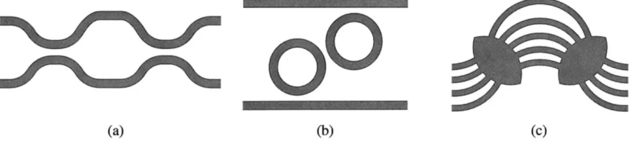
In addition to bends required to route waveguide paths between components on a densely integrated optical circuit, Fig. 1-1 shows several basic components of planar integrated optical circuits whose size critically depends on the bend radius: a directional coupler-based Introduction: Integration of Optical Devices in Silica 16
(a) (b) (c)
Figure 1-1: Some integrated optical circuit components for which bending radius is an important
factor for integration density: (a) Mach-Zehnder interferometer from two cascaded directional couplers, (b) second-order ring resonator channel add/drop filter, and (c) the Arrayed Waveguide Grating multiplexer/demultiplexer.
Mach-Zehnder interferometer, a ring resonator channel dropping filter, and an Arrayed
Waveguide Grating (AWG) - an integrated wavelength multiplexer/demultiplexer based on
wave interference. Proposed in 1988 by Smit [56], the AWG, also known as the Waveguide Grating Router (WGR) and Phased Array Grating (PHASAR), has become one of the most practical and promising integrated optical components [67],[64],[13]. Primarily implemented in silica, it is commercially available from, among others, Lucent Technologies, Hitachi and NT&T/PIRI. One of the limiting factors in the size of the AWG is the minimum bend radius of the "grating arm" waveguides. Keeping the bend loss within acceptable bounds can limit the bend radius to over 5mm, while junction loss that results at straight-bent waveguide interfaces can further push the minimum bend radius to over 10-15mm [8].
A technology that allows a drastic reduction in the bending radius would overcome one of silica's major obstacles to attaining truly large-scale optical integration. We propose a scheme using air trenches to provide locally enhanced lateral mode confinement. Air trenches have been investigated in the past in the context of bend loss (e.g. [73]), and have been used to make compact bends in ridge waveguides (referred to as deep etching in that context, [59],[47]). For low index contrast buried waveguides (e.g. silica), large junction losses occur at the interfaces between the straight silica waveguide and the air trench. We introduce a new "cladding taper" to remove abrupt junction-induced mode mismatch and Fresnel reflection in order to miniaturize optical waveguide bends while preserving low-loss performance [49].
At the time of writing of this thesis, new results were published by den Besten et al. on a low-loss (<4dB), compact (1mm x 1mm) 8x8 AWG in indium phosphide (InP) ridge
Introduction: Integration of Optical Devices in Silica
waveguides, by the use of deep etching [12]. This is precisely the type of application aimed at in buried silica waveguides with the work in this thesis.
1.2
Previous Work on Dense Integration, Sharp Bends and
Air Trenches
Prior to delving into the design of small Air Trench Bends for buried silica waveguides, we review the previous work on dense integration, sharp bends and air trenches.
While silica PLCs in general have low integration density with component sizes on the order of centimeters [42], high index contrast platforms such as silicon-on-insulator (SOI) offer very dense integration. Sharp, low loss 90 bends, on the order of a wavelength in radius, have been proposed for SOI [31], shown in Fig. 1-2d. Their operation is based on a low-Q resonant cavity, but also relies on bend-guiding and corner mirror reflection (like Fig. 1-2b). A detailed description of ultra-compact components in high index contrast is given in [30]. However, high index contrast platforms pose challenges of fiber-to-chip coupling loss due to mode shape mismatch and misalignment because waveguides are small (e.g. -0.2pm). They also have high scattering loss and sensitivity to other fabrication defects and tolerances, and pose fabrication processing challenges. The case is similar with high contrast, forward looking platforms like photonic crystal waveguides [40] (Fig. 1-2e).
In low index contrast, integration density is limited by, among other factors, the mini-mum bend radius for acceptable loss. An extensive literature exists on the analysis of bend loss ([32],[18],[47],[16],[53]). In bends which terminate in straight waveguides, there are ad-ditional contributions to total loss from scattering at the straight-bent waveguide interfaces, due to mode mismatch. To reduce this "junction loss", a lateral offset between the straight and bent waveguides was proposed by Neumann [45], to align the laterally shifted modes of the straight and bent waveguides. Pennings showed that, in addition, the widths of the straight and bent waveguides should be unequal for optimum mode matching [47].
Numerous techniques for the reduction of loss in bent waveguides of small bend radii have been proposed. In 1986, Korotky et al. proposed a "crowning" technique which formed
increased-index triangular prisms in the core of a LiNbO3 diffused waveguide bend, in order to steer light and reduce bend loss at small radii [24] (Fig. 1-2a). They achieved a three-fold reduction of radius (to 5.5mm) in comparison to standard LiNbO3 bends, with a loss of 18
1.2 Previous Work on Dense Integration, Sharp Bends and Air Trenches
(a) (b)
(c)
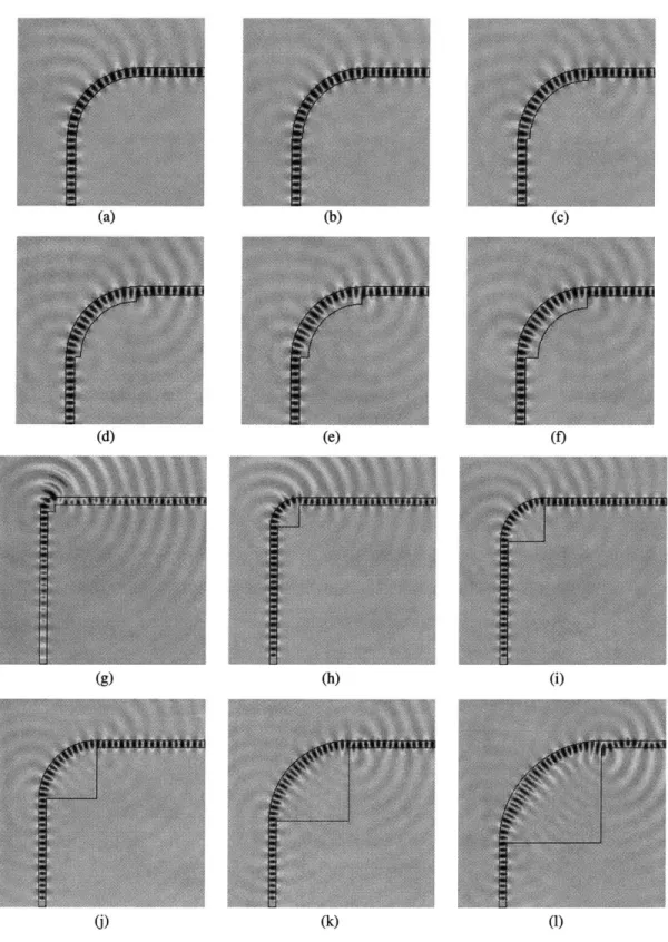
(d) (e)
Techniques for low-loss sharp bends in: low index contrast - (a) "crowning" in LiNbO3 diffused waveguides [24], (b) corner mirrors [2],[59], (c) doubly-etched bends for ridge waveguides (with waveguide cross-sections before and in the bend); and high index contrast - simulations of a (d) low-Q resonant cavity bend for SOI waveguides [31], and (e) 2D photonic crystal waveguide bend [40], both with high transmission efficiency.
~0.1dB.
More recently, several techniques for the better quality, lithographically etched waveg-uides have been proposed. One of the first was the use of etched-wall corner mirrors, proposed by Benson [2] (Fig. 1-2b). Such corners have not been able to yield losses much lower than -1dB [59], so attention turned back to the design of efficient curved waveguides. The introduction of an asymmetric cladding or air trench into bent waveguides has been studied by numerous authors (e.g. [73]) as a method to reduce bend loss by artificially increasing the index contrast at the outer radius. Pennings described an extension of the air trench to ridge waveguides [47]. Referred to as "doubly etched" (or deep-etched) bends, these were fabricated by Spiekman et al. [59] achieving compact radii (30pm) with rela-tively low loss (0.6dB total loss, 0.2dB bend loss only) in InP/InGaAsP ridge waveguides.
Figure 1-2:
Introduction: Integration of Optical Devices in Silica
Results on an Arrayed Waveguide Grating mux/demux using such ridge waveguide bends in InP were recently published [12].
Although bend radius can be reduced, a significant loss in all air trench-aided bends is the junction loss between the low index contrast waveguide and the air trench section, due to mode mismatch and Fresnel reflection. This problem is particularly serious in silica index contrasts, where junction loss is estimated to be limited to >0.1dB per junction, when optimized.
In this thesis, an Air Trench Bend structure is proposed for silica buried waveguide PLCs which uses air trenches to achieve tight bend radii, and eliminates abrupt junctions between the trench and silica waveguides by employing a new "cladding taper". This taper ensures an adiabatic transition can be achieved between the low and high index contrast regions. The geometry proposed is general in the loss-for-size tradeoff, in that a set of dimensions for this geometry can be found for any desired bend loss value with no fundamental lower limits on the loss. Furthermore, the tapers allow the use of bend radii limited by bend loss and taper-bend junction loss rather than the silica-air trench junction loss. As well, the air trench waveguide is etched well below the core. It is shown that in this manner the substrate leakage in the air trench region can be reduced to arbitrarily low values.
Chapter 2
Analytic Tools for
Planar Waveguide Structures
In this chapter, analytic tools are discussed for the analysis and design of the integrated optical structures (air trench waveguides, bends, cladding tapers) presented in Chap 3. Modal expansion of fields is reviewed for lengthwise-invariant dielectric waveguides, though used also for bending waveguides in Sec. 2.5. The Finite-Difference Time-Domain method, a popular numerical simulation tool used for the simulation of all complex structures in this thesis, is briefly reviewed in terms of a discrete formulation of electromagnetic theory on a lattice. A vectorial mode solver for 2D cross-section waveguides which also follows from this discrete formulation, and is consistent with-FDTD, is described, and used for subsequent waveguide design. All FDTD simulations, as well as bend and junction loss analyses in this thesis are two-dimensional (2D). The Effective Index Method (EIM) is a commonly used and very accurate method for reducing 3D (2D cross-section) planar waveguides to equivalent 2D (ID cross-section) structures. The standard EIM and a perturbative correction applied for more accurate buried waveguide analysis are described.
We next discuss junction, bend and substrate loss. Focusing on 2D (ID cross-section) waveguides, we consider junction scattering at interfaces between dissimilar straight waveg-uides, as well as at junctions between straight and bent waveguides. We then discuss bend loss in circularly bent slab waveguides and single boundary bends under whispering gallery operation. We review two very practical and insight-lending mode solution methods: WKB analysis, and boundary matching with Airy function form modal field solutions. The
de-pendence of bend loss on index contrast, radius, wavelength and bent waveguide width is reviewed. Finally, the optimization of bent waveguides which terminate in straight waveg-uides is described, considering bending and junction losses. From gained insight, an optimal geometry (in terms of total size for a given loss and index contrast) for a bend terminating in straight waveguides is suggested.
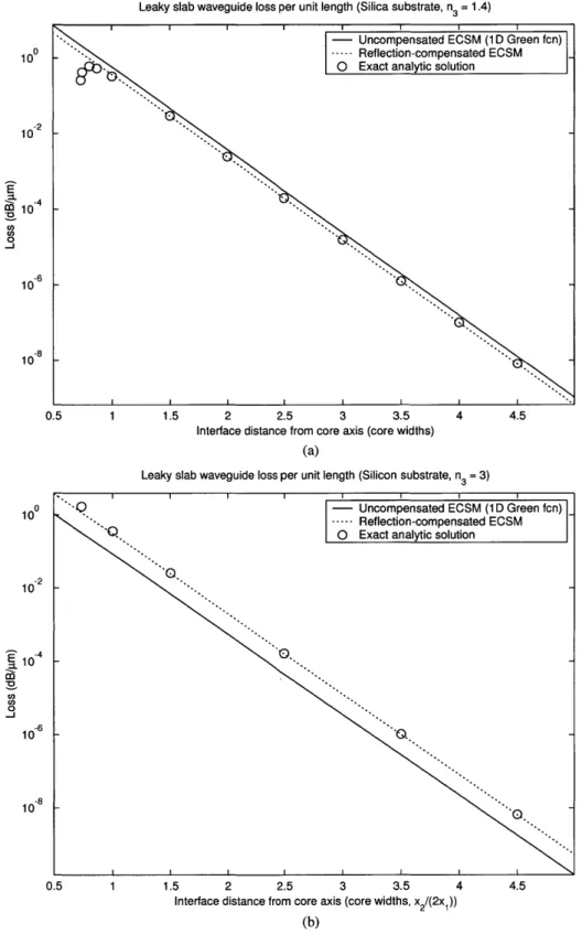
The treatment of the above structures in 2D by the Effective Index Method ignores possible leakage loss to a substrate. Substrate loss of 3D (2D cross-section) waveguides is treated last, by an equivalent source method with perturbation. In the analysis, a dyadic Green's function is integrated over a source equivalent to an ideal, guiding waveguide, to find the radiation field in the leakage loss region perturbed to represent the actual, leaky waveguide. The method is also applied to a 2D (ID cross-section) example with an analytic solution, for a validity check of the approximate method.
2.1
Modal Expansion of Fields
Analysis of electromagnetic field propagation in straight (e.g. z-invariant in Cartesian coordinates) structures is conveniently described in terms a set of guided and radiation modes. Mode solution and field expansion in dielectric waveguides is well-covered in liter-ature ([39],[43],[65],[58]). We briefly review it here, starting with Maxwell's equations for isotropic media in time-harmonic form (e.g. [23]),
V x E = iwpH (2.1) V x H= -iWfE+
f
(2.2) V - CE = p (2.3) IP -p 0with electric and magnetic field phasors, E and H, volumetric current density J and charge density p, and the permittivity e and permeability /t all spatially dependent in general. For p constant, propagation of the electric field is described by the vector wave equation resulting from the curl equations (2.1) and (2.2),
V x V x E - k2 = ipJ (2.4)
with dispersion relation k2 = W2pE.
Eigenfunctions of the Source-Free Vector Wave Equation
Modes are the eigenfunctions E of the source-free electric field vector wave equation
(f
= 0). In a z-invariant structure, E = E(x, y) and E(x, y, z) = E(x, y)eiz, where each mode is associated with a propagation constant (eigenvalue)p.
Using the simple z-dependence, the wave equation for modes of the structure can be formulated in terms of two out of the six E and H field components. In terms of the transverse electric field components Ex(x, y) and E.(x, y) the vector wave equation is
22\&/ Dc 1 &c\
-2
2!3- - 2EX(25
VS+ 2Ex + a1Ex aE+ -Ey - =#2E (2.5)
ax E ax E ay
(Ey
+ Ey + +3 E ) = 2Ey (2.6)and the third component (Ez) is determined by Gauss' law (2.3), while the magnetic field results from Faraday's law (2.1). Alternatively, a wave equation can be obtained in terms of transverse magnetic field components (Hx, Hy), or the longitudinal electric and magnetic fields (Ez, Hz). The wave equation can be written more compactly in operator form [72],
FX
PX
Ex
1
=02 E~
E (2.7)PYX
vYY Ey EyThe modes are found by solving for the eigenfunctions/values of this matrix equation. The eigenvalue equation for 3 is set by the determinant of the matrix P - 321,
D(O) = PX PXY -2T
=o.
Pyx
PyyWe solve this determinantal equation numerically by discretizing the operators P as shown in Sec. 2.2.3. The D(O) notation is used later in solving for leaky modes of straight and
bent structures (Sec 2.6.1,2.5).
In the one-dimensional (e.g. slab) waveguide case, &/&y = 0 and (2.5),(2.6) degenerate to the familiar slab wave equations for the TM and TE polarizations, respectively,
2 + k2 Ex + IEx
= 2
EX (TM)
(2.8)
2 + k EY = /2EY (TE) (2.9)
The equations for the two polarizations are decoupled in the 1D waveguide. This is not so in the general 2D waveguide, where (2.5),(2.6) must be solved simultaneously for modes.
Sometimes a semi-vectorial approximation is made to the wave equation set (2.5),(2.6) to decouple them for two principal polarizations, termed quasi-TE and quasi-TM [61],[68]. Neglecting a field component contribution in each equation (Ey -+ 0 in (2.5), E - 0 in
(2.6)), the decoupled wave equations are
P..E. = # (Eys 0) quasi-TM
PyyEy = 6(E , I 0) quasi-TE.
This is usually a fairly good approximation as can be seen from the relative mode component amplitudes plotted for the modes of a waveguide in Fig. 2-2.
Orthogonality of Modes [381
For z-invariant structures, an orthogonality relation can be defined for the guided and radiation modes [38]. For forward guided modes in lossless waveguides it is given by
S
(Em
x H*)where P is the guided power of mode m = n. For orthogonality relations among radiation
modes, or between guided and radiation modes, see e.g. [38]. Orthogonality is useful in the projection of an arbitrary field distribution onto the basis set of modes. For an arbitrary electric field distribution at z = zo in a lossless waveguide (satisfying Gauss' law, of course), and its corresponding magnetic field from eqn. (2.1),
E(x, y, zo) = (an + bn)En(x, y)
n
N(x, y, zo) = (an - bn)Hn(X, y)
n
the individual mode amplitudes an for guided modes are given by
a = ' x *) - da+ I* x H -da
b = 1 f x
N*)
- da f\EZ
x - da.2.2
Mode Solvers and FDTD
Numerical methods are necessary for simulation of the dielectric optical structures consid-ered in this thesis. Design and modeling of waveguides with a 2D cross-section requires an
accurate method for obtaining their modes.
It is known that idealized 1D cross-section slab waveguides have simple analytic mode solutions (e.g. [17],[23],[39]). The eigenvalue equation for the propagation constants is transcendental, but relatively easy to evaluate. General multilayer slab (ID cross-section) waveguiding structures have fully decoupled determinantal equations for TE and TM modes, conveniently reduced to the scalar wave equation (with a slight modification for TM), as pointed out in Sec. 2.1. Multilayer ID waveguides have simple analytic forms for the mode field solution in each layer, and a simple analytic determinantal equation. Solving for the modes of this type of structure is not pursued here, but the solution follows a similar line of reasoning to the mode solution for the 1D leaky waveguide presented in Sec. 2.6.1.
Waveguides of 2D cross-section do not in general have simple solutions, and much literature exists on numerical methods for finding the modes. They divide into scalar, semi-vectorial (approximated for decoupled TE/TM equations) [61] and full-vector (most accurate) methods [72]. Among the numerical approaches taken are circular harmonic ex-pansion [15] or free-space mode matching, finite difference (e.g. [61],[72],[51]) and finite element methods, and the spectral index method (e.g. [68]).
We use a full-vector mode solver based on an accurate and self-consistent finite-difference formulation of Maxwell's equations [9], which obey a full set of discrete conservation laws. This is exactly the Finite-Difference Time Domain algorithm ([74],[63]), commonly used for simulation of microwave and optical wave propagation in structures of arbitrary dielectric distribution. We use 2D FDTD for the simulation of all structures in this thesis.
2.2.1 Electromagnetic Theory on a Lattice [9],[74]
A discrete electromagnetic theory, defined on a lattice, has been formulated by Chew [9] in a very compact and intuitive form. Replacing differential equations with difference equations, it obeys a discrete law of charge conservation, and has an equivalent reciprocity theorem, Poynting's theorem and uniqueness theorem. This theory is of great use in numerical modeling because it applies to a discretized grid and gives rise to no spurious solutions or
instabilities as guaranteed by its discrete conservation laws.
It is based on a discrete version of vector calculus with discrete forms of Gauss', Stokes' and Green's theorems and Huygens' principle, and is described in detail in [9]. We quote only the resulting discretized Maxwell's equations,
VxH
2 = Jm2V.B7 M
V m = PM (2.10)
with constitutive relations
B m 1 fm Bm±
Dm Em B 1
where ft and I are the spatially dependent permeability and permittivity tensors. In the above discrete formulation, integer vector m = (in, p) is the spatial grid variable while integer 1 is the temporal grid variable, with uniform spatial grid spacing A = Ax = Ay = Az and time t = lAt (Fig. 2-1a). E, B, H and D are vector variables with spatial (m) and temporal (1) dependence. Finally, peculiar to this discretization is the use of the tilde (~)
symbol on field quantities to indicate "fore-vectors" with :, and i components defined at grid points (m + 1/2, n, p), (m, n + 1/2, p) and (m, n, p + 1/2). The hat (^) similarly denotes "back-vectors" with the components defined at (m - 1/2, n, p), (m, n - 1/2, p) and
(*, n, p - 1/2) (Fig. 2-1b). Likewise, tilde and hat define partial derivatives as forward and backward differences, e.g. 5tFt = (Ft+l - Ft)/At. The del operator is defined in terms of
corresponding partial derivatives, e.g. V = s5& + 6y + 2z.
With this type of discretization, illustrated in Fig. 2-1, all derivatives are central dif-ferences, resulting in an O(A 2) numerical accuracy with respect to continuous Maxwell's equations. The arrangement also makes possible the fulfillment of the discrete conservation laws mentioned above.
This formulation is precisely the FDTD algorithm first proposed by K.S. Yee in 1966 [74]. We use FDTD for simulation of all structures studied in this thesis. We also use a finite-difference vectorial mode solver for 2D cross-section waveguides, based on the above discrete equations in time harmonic form, which is consistent with FDTD (based on [51]).
2.2 Mode Solvers and FDTD 27 z ----m,n,p+1) Y
~-
------ - m- 2n12p 12 (m-1 ,n+,p+ ) x (m+%n'-Mp+%)(m S-+ n+1,p) (m+1,n,p) - + ,n+,p-2) (a) mi (m,n,p) (b)Electromagnetic theory on a lattice: definitions of (a) interleaved grids m and m
+
-1;and (b) the corresponding electic field "fore-vector" (Em, after point m) and magnetic field "back-vector" (Hm+.I, before point m
+
1), associated with m and m + 1.2.2.2 Finite-Difference Time-Domain (FDTD) [74],[63]
The Finite Difference Time Domain (FDTD) method is a popular, numerically rigorous method for simulation of dielectric optical structures, particularly where high index contrast is present and the Beam Propagation Method (BPM) [75] is not applicable [63],[74]. FDTD can be used to simulate propagation in structures with arbitrary dielectric distributions.
Two-dimensional (2D) FDTD code, developed by C. Manolatou [30], is used for the simulation of structures in this thesis (structures are reduced to 2D using the Effective Index Method, Sec. 2.3). The edges of the computational domain are terminated using the perfectly matched layer (PML) absorbing boundary condition [3], and a discretization of
10-20 pixels per wavelength is used for accurate modeling. The details of the implementation, including the time step At for stability of FDTD, sources, and measurement of spectral response, are discussed in [30] and in the FDTD literature [63]. In our simulations, a pulse spanning the spectrum of interest is launched into the optical structure, and the entire spectral response with respect to the ports of interest is obtained in one simulation, which is terminated after the launched pulse has left the computational domain, and all significant residual electromagnetic power has decayed. The FDTD simulations in this thesis were carried out on a Cray T-90 supercomputer, using 64-bit floating point precision.
Figure 2-1:
Analytic Tools for Planar Waveguide Structures
2.2.3 Vectorial 2D Cross-section Waveguide Mode Solver [51]
A numerical finite-difference mode solver based on the discrete Maxwell's equations (2.10) in time-harmonic form was described in [51]. Such a mode solver is consistent with FDTD, and its modes are ideally suited to the excitation of waveguides in FDTD, with no residual power. Such a mode solver was implemented in this thesis for the design of 2D cross-section waveguides. It is briefly described, and some example modal solutions of air trench
waveguides used later in this thesis are shown.
The discrete vector wave equation for modes of a z-invariant structure, resulting from the time-harmonic form of (2.10), and given in terms of transverse field components is [51]
Mms
.X 1 S X E-m -V, ms- 8 EmEm - k2Enm
+
kEm=
0 (2.11)M+ IVS X XH18 s/Lk 2 H _k k2
Hs
, s m jVs 1 p+1H - + Hs Z 1
with propagation constant kz, and s indicating transverse field vectors. These equations can each be represented as a matrix eigenvalue problem for the modes of the form [51]
Ice -Es. -ki Es
In what follows, we use the first (transverse electric field) form of the eigenvalue problem.
Slab (1D Cross-section) Waveguide Discrete Eigenvalue Equation
Consider first an arbitrary ID cross-section waveguide with dielectric profile Em = (x), p constant, and &, = 6, = 0. Eqn. (2.11) results in two decoupled eigenvalue equations, one for each polarization, as expected in the 1D cross-section problem (compare to (2.8),(2.9)),
5x EmE +k 2Ex' = k2Ex"i (TM)
XOXEY+
k2EL
=k
Ey(TE)
where
E
= -E + 9E , and the y- and z- dependences have been removed from the mode field in the equation (indices n,p). The equation above is. the discrete version of the scalar (modified) wave equation for TE (TM) modes of 1D cross-section structures in Sec. 2.1. Step-index ID waveguide mode solutions have a simple analytic form, and can be solved more efficiently using other methods, but the equation above applies to arbitrarydielectric distributions.
2.2 Mode Solvers and FDTD
2D Cross-section Waveguide Discrete Eigenvalue Equation
The 2D cross-section waveguide is of most interest in this thesis for the design of rectangular silica and air trench waveguides (Chap. 3) because simple, exact analytic solutions do not exist. In terms of the transverse electric field, eqn. (2.11) yields a matrix pair of eigenvalue equations where the two transverse electric field components are coupled,
- x Em-
k2
E +[Dy x
XIyEm
Elm' = -k E[-mo Em .
- ~ ± -
k1
E5"8-B 1 6Em Ex + [-6x28- 5y 6 'Edm- k 2Em = - k 2EY
Em .
E
mI Mand can be represented as a matrix eigenvalue equation (compare (2.7))
Pix Ek2 EM
prp~1.
=-ki
-l
P MY P& EY -m EM
This matrix is of size (M x N)2, where the computational domain is sized M x N. We
implement a perfect electric conductor (PEC) boundary condition at the edges of the cop-mutational domain. A number of methods can be used to find the eigenvalues, kz, and eigenvectors (mode fields) of the above operator. An efficient algorithm is described in [51]. We simply use MATLAB's sparse matrix eigenvalue solver that uses the Arnoldi algorithm.
2D Mode Solutions of Example Silica and Air Trench Waveguides
We use this mode solver to find the guided modes of the waveguiding structures in this thesis: buried, square core silica waveguides; and, ideal air trench waveguides (see Fig. 2-3c, Sec. 3.3).
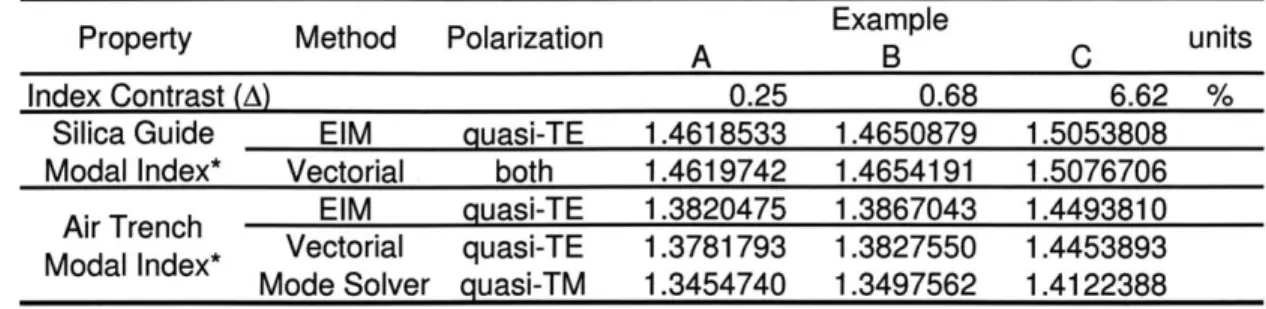
Fig. 2-2 shows the electric field distributions of the lowest order guided mode, of each polarization, in an ideal air trench waveguide. The parameters of this waveguide are given under Example C in Table 3.2. Contour plots of the fundamental dominant electric field component for each polarization, for all three air trench waveguide examples used in this thesis are given in Fig. 3-5. Computed propagation constants are used to evaluate the accuracy of the approximate Effective Index Method in Sec. 2.3 (see Table 2.1).
Analytic Tools for Planar Waveguide Structures Quasi-TE E -o Quasi-TM Ex (dominant) =i 0.8 0.4--0.2 -0.02 0.01 -0.01 15 -0.02 05 -1 - -- 0.5 y( m -0.5-0 .1 X (A ) 0.5 -1.5 E y(dominant) 0.8 -U0.4,,
.
RD0.2 05 LL - 0 -1 -0.5 -0.6 y( 0-1 X(pm) 0.5 -1.5 Ez 0.15 0.1 0.05 d0 75 -0.05 -- --LL -0.1 -0.5 -0.15 0 - -.5-0.5 y (Am 0 1 X (AM) 0-5 -1.5 0.04-1.5 0.02 -0.02-1. -0.04 M)-1 -- 0 -0.5 -0 - -AM 0 -X (Am) 0,5 -. Ez 0.3 - -0.2 0.1 1.5 -0.11. . -0.2-- --0.3 -- 0.5 -0.4 ...-- 0 -0.5 --. X (pM) 05-1.Figure 2-2: Electric field component disributions for air trench example waveguide C (Table 3.2); (a)-(c) Quasi-TE, and (d)-(f) Quasi-TM fundamental mode distributions.
30
uu~i~T - - _______
31
(a) (b) (c) (d)
Figure 2-3: Effective Index Method: (a) buried, (b) rib, and (c) air trench waveguides can be reduced to (d) an equivalent slab waveguide with effective indices.
2.3
Effective Index Method [22],[65]
All integrated optics problems are physically posed in three dimensions. Analytic tools for 2D structures, however, are much simpler and thus more powerful. A very successful technique used to reduce 3D waveguides to equivalent 2D (slab) waveguides, introduced by Knox and Toulios [22], is known as the Effective Index Method. A detailed treatment is given in [65]. The EIM is difficult to derive as an approximation to an exact mathematical formulation, but has great intuitive appeal and has proven very accurate, particularly for rib, ridge and even buried waveguides (e.g. [65],[76],[48],[39]).
The EIM simplifies the 3D waveguide to an equivalent slab waveguide by collapsing the third ("vertical") dimension out of the way. This is done by solving the slab waveguide problem in the vertical (y in Fig. 2-3)direction, and using the mode's effective index, 3/ko, for the index of the equivalent slab in the appropriate region (here 1, 11 or III) [65],[39], [76]. For buried waveguides, this cannot be done in the cladding where no guided slab mode exists in the cladding cross-section, so the lateral cladding index is not modified in the equivalent waveguide. Better results are obtained by using a perturbative correction to the Effective Index Method that yields effective indices for the lateral cladding.
We use the Effective Index Method in this form for all waveguides in this thesis, straight and bending. However, for bent waveguides the correct formulation of the Effective Index Method is slightly different, as pointed out in [47]. We disregard this in our calculations.
2.3.1 Standard Effective Index Method [22]
The original EIM was proposed for use in buried waveguides [22], where an effective index
N, is found for the core, but the cladding index is not modified, Ne1 = nci. However, it is
Analytic Tools for Planar Waveguide Structures
in rib waveguides that it has found much use, and shown great accuracy.
We consider the fundamental guided mode. The rib waveguide in Fig. 2-3b is divided into three lateral regions to correspond to the equivalent slab in Fig. 2-3d. The effective index of the equivalent slab is then assigned the value of the modal index of the fundamental mode of the slab waveguide in the vertical cross-section for the corresponding region. The problem is thus reduced to 2D. The propagation constant of the rib mode can be approximated by solving for that of the equivalent slab [65].
To stay consistent with quasi-TE and quasi-TM mode polarizations, the Effective Index Method is applied to collapse the third (y) dimension using TM boundary conditions if the equivalent waveguide is to be used in TE configuration, and vice versa.
2.3.2 Perturbation-corrected Effective Index Method [11]
The structures of interest in this thesis are buried (Fig. 2-3a) or air trench (Fig. 2-3c) waveguides, which do not have guided slab modes in the y-section of the lateral cladding regions, for purposes of the Effective Index Method.
Here, the core effective index is found by the regular EIM, while the cladding effective index, Nd, is calculated as a perturbative correction of the former. The assumption made is that the cladding region has a y-dependent field distribution identical to that in the core, and only the perturbation of the propagation constant due to a different index distribution in the cladding is calculated. The perturbatively calculated effective cladding index, Ni, is
Ne, = NcO - AN
with
-1 2 (Y)ID(Y)12dy
2NcO0
J7(Y)2dy
Ari(y =ni~y - rij(y) = rijII(y) - ni(y
where I(y) represents the field distribution from the effective index calculation in the core region I. A more detailed treatment can be found in [11],[30].
For three example buried silica waveguides (Fig. 2-3a), in Table 2.1 we give comparison of the perturbation-corrected Effective Index Method modal index solutions to the numer-ically exact modal index obtained using the vectorial mode solver from Sec. 2.2.3. The 32
2.3 Effective Index Method [22],[65] 33
Table 2.1: Effective Index Method and Vectorial Mode Solver Propagation Constants
Property Method Polarization A Example C units
Index Contrast (A) 0.25 0.68 6.62 %
Silica Guide EIM quasi-TE 1.4618533 1.4650879 1.5053808
Modal Index* Vectorial both 1.4619742 1.4654191 1.5076706 Air Trench EIM quasi-TE 1.3820475 1.3867043 1.4493810 Modal Index* Vectorial quasi-TE 1.3781793 1.3827550 1.4453893
Mode Solver quasi-TM 1.3454740 1.3497562 1.4122388
*Straight waveguides with cross-sections as in Fig. 2-3a,c. Dimensions for examples A-C given in Tables 3.1, 3.2. Calculated indices at free-space wavelength of 1550nm.
x-dependent modal field distribution of the equivalent slab waveguide is compared to the 2D solution from the vectorial mode solver along the x-axis in Fig. 2-4, for the case of the Air Trench Waveguide (Table 3.2) of example A (silica contrast of A = 0.25%). It shows very good agreement. The equivalent waveguide is used in 2D FDTD simulations of the structures in this thesis, and it is important that both the modal index and field distribution resemble the original 3D waveguide.
EIM Slab Mode 2D Vector Mode 0.8 -S0.6 --E co
0.4-0.2 - -/ .,/... llilllli / -.. A:.rerA 4 \ 0 ' -3 -2 -1 0 1 2 3 Displacement (microns)Figure 2-4: Lateral (x-axis) field distributions of the Air Trench Waveguide of example A (Ta-ble 3.2) using the 2D cross-section vectorial mode solver (dashed line), and that of the equivalent slab waveguide obtained using the Effective Index Method (solid line).
34 Analytic Tools for PlanarWaveguide Structures
(a) (b) (c) (d)
Figure 2-5: (a) Multi-junction dielectric stack with mode rays indicated, and (b) straight-straight, (c) straight-bent and (d) bent-bent waveguide junctions. Forward and backward am-plitudes of the nth mode in regions 1,2 are indicated in (b),(c).
2.4
Junction Loss at Waveguide Interfaces [65],[47],[5]
Junction analysis investigates scattering at an interface between two different structures, for each of which a set of modes describes propagation relative to the interface. A simple example is a (ID) dielectric stack, for which the modes in each layer are plane waves; more complex junctions are shown in Fig. 2-5. A scattering matrix formalism is convenient, where the solution is obtained by expanding the field distribution on either side of the junction in terms of the its modes and matching the boundary conditions using this expansion. An extensive literature is available on scattering and transfer matrix methods for analysis of junctions (e.g. [65],[47],[5]). Concepts of use in this thesis are briefly summarized.
The full potential of planar junction scattering analysis is realized in its application to lengthwise(z)-varying structures such as step-index waveguide tapers and directional cou-plers [39], and recently to more complex structures like photonic crystals [5]. By discretizing the z-varying structure into a large number of short z-invariant sections, the behaviour of the total structure can be obtained by cascading a set of transfer matrices, obtained in terms of the Local Normal Modes of each section [39]. The scattering parameters of the entire structure can be obtained at the end by converting the total transfer matrix to a scattering matrix (e.g. [50]).
In this thesis, we are primarily concerned with single abrupt junctions between dissimilar straight or straight and bent waveguides, in the context of optimizing the transfer of power from a chosen source mode in one waveguide to a target mode in a second waveguide. Only
2.4 Junction Loss at Waveguide Interfaces [65],[47],[5]
two-dimensional (slab) waveguide problems are considered, with the Effective Index Method used to reduce 3D problems to 2D (see Sec. 2.3).
2.4.1 Junction Scattering via Mode Expansion and Transfer Matrices
Consider the junction of the two z-invariant slab (layered, in general) waveguides in Fig. 2-5b. The TE modes of each waveguide are fully described by the electric field distribution
lein)eiz, a single scalar distribution for one vector component ( in Fig. 2-5b). The set
of modes (these scalar distributions) is composed of guided and radiation modes, and is a complete and orthogonal set. The transverse fields at each side of the interface z =
0+,-are represented as a superposition of the modes of each structure,
Ei = Z(ain + bin)Iein)
n
HiX=
-E
An(ain-bin)Iein)n
W-in regions i = 1, 2, with forward and backward mode amplitudes ain and bin, respectively,
for the nth mode, and modal field Iein) = ein(x). By matching these fields at the boundary, and making use of orthogonality relation (eimlein) = 6mn, a transfer matrix to find mode amplitudes in region 2 given those in region 1 is obtained (refer to Fig. 2-5b),
[
2 = F 1=T - I
b2 b
where, for example, d2 is a "vector" of amplitudes of all modes a2n, or, for a single mode
in region 2,
a2m
1
Fi1
1 T mn Tm1F ain= Tmn -[=
b2m n b 2(e2mle2m) n T T bin
with matrix elements
Taa Mn = T bb mn = \ 1 + 32m /e2len(emein)
T a = T ba = 1 - Oin
(e2mlein)-The 1D overlap integral above is defined as
(e2mlein) = Jesm()ein(x)dx.
Transfer matrices are handy because they can be cascaded easily with free-space propagation and other junction transfer matrices to yield a total system transfer matrix. However, out-going waves are not known at the outset, so a more desireable representation is a scattering matrix which gives outgoing mode amplitudes in terms of given incoming mode amplitudes,
bim
[
a1n Smnsmn
1
an
= ESmn- *
I
S2 s22=a2m n b2n n mn mn bin In terms of the above transfer matrices, the scattering matrix elements are
S" mn = T bb-1mn
S12 = - [Tbb] -I. rba
S 21 mnmn Taa - Tab mk -[Tbb]-1.Tbak1 1n
Smn =Tmank ' [T
kn-with the understanding that repeated indices imply Einstein summation (i.e. matrix mul-tiplication). This representation makes clear that the insertion loss between a source mode n and target mode m in regions 1 and 2 respectively, S21, is dependent not only on the overlap integral of those two modes, but of all modes, due to the second term in the
ex-=21
pression for S which involves the overlap integrals of all modes (if the T-matrices are not diagonal).
The above notation does not make explicitly clear the symmetry of the scattering matrix implied by reciprocity. Making use of the completeness property of the mode expansion ((e2mlelk)(elkle2n) = 6
mn, summed over k, for region 1) and of reciprocity, an explicitly
symmetric set of s-parameters is found by Pennings [47],
S = - (eikte2p)#2pq(e2qlelm) + #Ikm} {(ek e21)21r(e2rlein) + Likn
S2 n= (e2k~e1p)1pq(e1qle2m) + 2kmJ -12(e2ke11)O1n (2.12)
with the remaining two obtained by swapping indices 1,2 in the above expressions, and the propagation constant matrix /9imn = 3
im6mn. Einstein summation is implied. These
expressions have a more clear connection to the approximate junction loss formulas we will
use.
Suppose that the set of modes (eigenfunctions) is identical for regions 1 and 2, while
their respective propagation constants may or may not be the same. The overlap integral
2.4 Junction Loss at Waveguide Interfaces [65],[47],[5]
matrices (eimlejn) in (2.12) are then diagonal because all overlap integrals are zero, except for m = n when they are unity. In addition, the 3 matrix is diagonal by definition, so the
insertion loss s-parameter in this case simplifies to
S2 1 2 (e2mlelm) 31m
m - 2
01M
mm (e2mleim)/31m(eimle2m) + 02m /31m+/2m
This is valid for a dielectric stack (Fig. 2-5a) where modes are plane wave, and a single
plane wave in one layer excites one and only one mode in the following layer because of
perfect mode overlap. It is also possible in slab waveguides with the right constraints, and has been used to describe limits of fiber match to high index optical chips [44](p.103-4), and to design extremely low-loss, high strength integrated optical Bragg reflectors [66] and high-Q integrated Bragg resonators [70].
2.4.2 Straight-Straight Waveguide Junction Loss
It is of interest to us in this thesis to evaluate the insertion loss as defined in the context of
transfer of power from a source mode in region 1 to a chosen destination mode in region 2.
To avoid the necessity to compute a large (ideally infinite) number of modes, as required by expr. (2.12), we make a simplification by assuming that the overlap integral of the source mode with all modes in region 2 except the destination mode is very small. This is consistent with a "low-loss" junction. Then the reflection modes of region 1 are all neglected in matching the boundary conditions, except the reflection into the source mode
=21
in the reverse direction. A simple formula for the S parameter results,
S2 = 2I31n 2) (e2mleln) (2.13)
mn \ 1n + 02m ) (e2mle2m) The net power carried in the +z direction in a mode is
Pik = (Iaik12 -| bik 2) Oik (eikleik).
2wp-Assuming no incident mode amplitude in region 2 (b2n = 0), normalizing only to the incident
source mode power in region 1, and using (2.13) the insertion loss is
21 02m 2
#1n
2 (e2mlein)2lqmn(ss) = . 2.4
mn k 1 + /2mJ (e2mle 2m)(einlein)(
Variations of this formula are common in literature (e.g. [28],[18]). It is used for all straight-straight junctions in this thesis, and is valid for low loss. A comparison of junction loss 37
![Figure 2-8: WKB (solid blue) and Airy function (dotted red) solutions for the leaky mode distri- distri-bution of a single boundary bend (SBB), identical to the example in Table 5.1 in [47]](https://thumb-eu.123doks.com/thumbv2/123doknet/13912532.449045/46.918.140.763.119.629/figure-function-dotted-solutions-distri-boundary-identical-example.webp)
![[PDF] Manuel pour apprendre à utiliser iDVD 7 [Eng] | Cours informatique](data:image/gif;base64,R0lGODlhAQABAIAAAP///wAAACH5BAEAAAAALAAAAAABAAEAAAICRAEAOw==)