HAL Id: hal-02539646
https://hal.archives-ouvertes.fr/hal-02539646
Submitted on 10 Apr 2020
HAL is a multi-disciplinary open access
archive for the deposit and dissemination of
sci-entific research documents, whether they are
pub-lished or not. The documents may come from
teaching and research institutions in France or
abroad, or from public or private research centers.
L’archive ouverte pluridisciplinaire HAL, est
destinée au dépôt et à la diffusion de documents
scientifiques de niveau recherche, publiés ou non,
émanant des établissements d’enseignement et de
recherche français ou étrangers, des laboratoires
publics ou privés.
28 Gbps silicon-germanium hetero-structure avalanche
photodetectors (Contributed paper)
Daniel Benedikovic, Léopold Virot, Guy Aubin, Jean-Michel Hartmann, Farah
Amar, Bertrand Szelag, Xavier Le Roux, Carlos Alonso-Ramos, Paul Crozat,
Eric Cassan, et al.
To cite this version:
Daniel Benedikovic, Léopold Virot, Guy Aubin, Jean-Michel Hartmann, Farah Amar, et al.. 28
Gbps silicon-germanium hetero-structure avalanche photodetectors (Contributed paper). SPIE OPTO
Integrated Optics: Devices, Materials, and Technologies XXIV, Jan 2020, San Francisco, United
States. �10.1117/12.2543499�. �hal-02539646�
28 Gbps silicon-germanium hetero-structure avalanche photodetectors
(Contributed paper)
Daniel Benedikovic
a, *, Léopold Virot
b, Guy Aubin
a, Jean-Michel Hartmann
b, Farah Amar
a, Bertrand
Szelag
b, Xavier Le Roux
a, Carlos Alonso-Ramos
a, Paul Crozat
a, Eric Cassan
a, Delphine
Marris-Morini
a, Charles Baudot
c, Frédéric Boeuf
c, Jean-Marc Fédéli
b, Christophe Kopp
band Laurent
Vivien
aa
Université Paris-Saclay, CNRS, Centre de Nanosciences et de Nanotechnologies, 91120, Palaiseau,
France;
b
University Grenoble Alpes and CEA, LETI, Minatec Campus, F-38054 Grenoble, France;
cTechnology R&D, STMicroelectronics SAS, 850 Rue Jean Monnet, 38920 Crolles, France
ABSTRACT
Owing to its low-cost, high-yield, and dense integration ability, silicon nanophotonics is a good candidate to tackle the needs of exponentially growing communications in data centers, high-performance computers, and cloud services. Moreover, a number of nanophotonic functions are now available on a single chip, as they take advantages of silicon-foundry process maturity and epitaxial germanium integration. Optical photodetectors are key building blocks in the library of group-IV components and their performances are quite successful nowadays. In particular, silicon-germanium waveguide-integrated photodetectors are fixing new standards for next generation of on-chip interconnects in terms of compactness, speed, power consumption and cost. Indeed, conventional pin photodetectors yield good responsivities (~1 A/W in a 1.5 µm wavelength range), high bandwidths (~50 GHz), and dark currents well below 1 µA. Despite recent advances, their optical power sensitivities remain rather modest and speeds are limited to 25 Gbps only, however. Compensating for the insufficient photodetector sensitivity requires higher transmitter output powers and therefore higher energy consumption. Additional energy savings can be obtained by eliminating receiver electronics. Alternatively, an appealing approach is to exploit device structures with an internal multiplication gain to lower even more the power budget and improve energy efficiency of chip-based optical links. In this work, we report on waveguide-integrated photodetectors with lateral silicon-germanium-silicon heterojunctions. Here, we present avalanche photodetectors fabricated on 200-mm silicon-on-insulator wafers using complementary metal-oxide-semiconductor-compatible processes. Devices operate in the low-gain-regime to facilitate high-speed link operations at 1.55 µm wavelengths. An error-free signal detection was achieved at 28 Gbps, with power sensitivity of -11 dBm for 10-9 bit-error-rate, which is a relevant link rate for emerging chip-scale optical interconnects.
Keywords: silicon photonics, complementary metal-oxide semiconductor technology, optical photodetectors, pin mode operation, avalanche mode operation, germanium, impact ionization, gain, gain-bandwidth product, high-speed links
*
e-mail: daniel.benedikovic@c2n.upsaclay.fr
1. INTRODUCTION
Photonic integration technologies are essential for the realization of optical chips and provide an access to many emerging applications. Foreseen applications range from environmental sensing and health monitoring, through object recognition and civil engineering, to optical communications and interconnects, to list a few. The latter areas are key drivers in the field of photonics integration, as optical interconnects are rapidly replacing traditional copper-based electrical wirings in a variety of chip-scale communication links. Indeed, photonic technologies are particularly promising for long-haul optical fiber systems, short-reach data centers, and clouds, among others. Dense integration is a natural route to tackle challenges associated with cost, portability, speed and bandwidth as well as power consumption1-4. Small-sized and high-performance photonic devices were recently integrated in a single chip thanks to a monolithic integration approach4,5. Such achievements were obtained with the help of two group-IV materials: silicon (Si) and germanium (Ge). Si is definitely an indirect bandgap semiconductor, while Ge is almost direct, with a lower bandgap
(0.67 eV 1.14 eV at room temperature). Ge thus provides singular advantages and complementarities over pure Si platforms. Group-IV nanophotonics therefore enable complex on-chip functionalities6-10, from light generation and modulation to waveguiding and light detection11-14.
Optical photodetectors, devices that convert light into an electrical signal, are crucial components in integrated optical circuits. They were extensively investigated since the late 1990s1,14,15-37. Group-IV optical photodetectors integrated in mature silicon-on-insulator (SOI) waveguide platforms provide many advantages. Their fabrication makes full use of mainstream Si complementary metal-oxide-semiconductor (CMOS) processes, with therefore reproducible yields. They can otherwise miniaturized and have potential for large-volume integration and therefore lower costs of ownership. III-V photodetectors on SOI substrates may be used as well, through hybrid or heterogeneous integration with bonding or direct hetero-epitaxy38,39. This, however, typically comes hand-in-hand with increased production costs, fabrication complexity and potentially CMOS line contamination. Therefore, the use of group-IV materials seems optimal for the future needs of monolithic chip integration.
Various types of waveguide-integrated optical photodetectors with a p-i-n structure have been studied the last 10 to 15 years. Since the first fabrication of waveguide-integrated diodes by Ahn, et al.19, a large number of homo-junction (full Ge structures)15-28 and hetero-junction (combined Si-Ge structures)29-37 devices have been proposed, fabricated and experimentally evaluated. Both types of devices make use of p-i-n junctions, with light absorption in the intrinsic zones. The overall performance of homo-junction photodetectors is limited by process issues (ion implantation for p- and n-doped regions and metal vias are performed in/on top of Ge) and optical considerations (ultra-weak optical confinement within the intrinsic zone). Such devices are typically less performant compared to their hetero-junction Si-Ge-Si p-i-n counterparts. Full-Ge p-i-n photodetectors have slower responses, decreased responsivity (quantum efficiency) and higher dark current levels15-28. In stark contrast, hetero-structured Si-Ge photodetectors take advantages of advanced fabrication processes. Hetero-junction devices are fabricated with full Si metal via-contacts and doping (by ion implantation)10. Such an approach avoids Ge process issues and simplifies the process flow. It otherwise yields, because of optical index confinement differences between Ge and Si, a much better light confinement in the intrinsic device zone, significantly improving photodetector performances. Hetero-structured Si-Ge photodetectors have already been demonstrated with significantly better performance metrics across the near-infrared (near-IR) fiber-optic communication wavelengths31-37.
Although promising, conventional p-i-n diodes typically provide only restricted levels of responsivity due to external quantum efficiency limits. From a system point of view, the device sensitivity for high-speed signals is quite modest in p-i-n photodetectors. Furthermore, simple p-i-n diodes also yield low electrical output levels. Because of that, extra electronic stages with trans-impedance amplifiers (TIA) or limiting amplifiers (LA) are typically attached to the devices. Improved performance photo-detectors can be obtained by switching over to devices that exploit an internal multiplication gain1,14,40-48, i.e. on-chip avalanche photodetectors (APDs). In the course of years, APDs have been fabricated with the following structures: metal-semiconductor-metal (MSM) or separate absorption charge multiplication (SACM). MSM devices are operated at low bias, with fabrication, which is compatible with CMOS tools. They however suffer from high dark currents and degraded sensitivity40. In contrast, SACM photodetectors benefit from a low multiplication noise thanks to the use of Si within the region of avalanche multiplication. However, devices with top-illuminated41,42 or waveguide-coupled43 architectures call upon high voltages, typically beyond 20 V, and still operate with a bit rate of 10 Gbps only. State-of-the-art Si-Ge APDs can nowadays be operated with voltages lower than 10 V. The working speeds are still limited to 10 Gbps44, 45 or 25 Gbps46-48, however.
In this work, we present recent results on compact photodetectors with lateral Si-Ge-Si p-i-n hetero-junctions. Photodetectors were fabricated on 200-mm SOI substrates using Si CMOS foundry processes. First, we comprehensively study the opto-electrical properties of waveguide-integrated photodetectors with different waveguide geometries. Photodetectors were operated under low-voltage supplies. At a 1 V reserve bias, devices exhibited dark currents between 5 nA and 150 nA, dark current densities between 0.404 A/cm2 and 0.808 A/cm2, responsivities (quantum efficiencies) spanning the 0.17 A/W - 1.16 A/W range (14% to 93% range), and -3dB bandwidths in the 7 GHz to 35 GHz range. Next, devices that operate in an avalanche regime were demonstrated, yielding improved signal quality for high-speed signal detections at 1.55 µm wavelength. An error-free signal detection was achieved at a link rate of 28 Gbps, with a power sensitivity of -11 dBm for a 10-9 bit-error-rate.
The manuscript is organized as follows. After the introductory Section 1, data on device dimensions, fabrication, and characterization are provided in Section 2. Section 3 reports on a low-bias operation of waveguide-integrated Si-Ge-Si
p-i-n photodetectors, while Section 4 presents recent results for avalanche-mode-operated Si-Ge-Si p-p-i-n photodetectors. Finally, conclusions are drawn in Section 5.
2. DESIGN, FABRICATION AND TESTING
Optical photodetectors with lateral Si-Ge-Si hetero-junctions are shown schematically in Fig. 1. Fig. 1(a) is a cross-sectional schematics of such a photodetector, while Fig. 1(b) is a top view of foundry mask layout. Optical microscopy images of some fabricated photodetectors can be found in Fig. 1(c)
Figure 1. (a) Cross-sectional schematics of a waveguide-integrated photodetector with a lateral silicon-germanium-silicon hetero-junction. (b) Top view of a mask layout with different photodetector geometries. (c) Optical micrograph image of a few fabricated photodetectors.
In this work, optical photodetectors are integrated at the end of SOI waveguides. A butt-waveguide-coupling is used together with lateral p-i-n junctions . The 220 nm thick Si guiding layer is on top of 2-µm-thick buried oxide (BOX). The integration strategy facilitates the fabrication of small-footprint photodetectors at the end of good optical quality waveguides35. The Ge layer (i.e. the intrinsic photodetector region) is ~260 nm thick. This light-absorbing layer is selectively grown in narrow Si trenches. the remaining Si thickness at the bottom of those trenches is about 60 nm. The active layer is embedded between p-type and n-type Si-doped regions with metal contacts formed on top. Variations in widths (wi) and lengths (li) of the intrinsic device region are included on the mask. Surface grating couplers are used to
inject light from an optical fiber into the Si chip. Surface grating couplers and Si interconnecting waveguides are designed to support transverse electric (TE) polarization at 1.55 µm. The injection Si waveguides are mono-mode, with a cross-section of 220 nm by 500 nm (thickness by width)35,36.
Optical photodetectors were fabricated using CMOS-compatible tools in CEA LETI's cleanroom facilitates on 200 mm SOI substrates. The fabricated devices were fully characterized in laboratories of Centre de Nanosciences et de
Nanotechnologies through static current-voltage measurements, small-signal radio-frequency testing, and large-signal
data link measurements for eye diagram acquisitions and bit-error-rate assessments, respectively. A detailed description of the manufacturing flow and the comprehensive opto-electrical characterization techniques used on devices can be found elsewhere35-37.
3. LOW-BIAS P-I-N MODE OPERATION
Dark- and photo-currents have been evaluated using current-voltage tests without and with light injected into the photodetectors, both as a function of the reverse voltage. Photodetectors of different widths and different lengths have been characterized, in this section, for a low-bias operation, ranging from 0 V to 3 V. Dark-current characteristics of different device geometries are shown in Fig. 2(a). Dark-currents under 1 V reverse bias remain consistently low (< 1 µA), typically of the order of a few tens of nA. The largest dark-current levels of around 150 nA are found for the largest devices (1 µm wide and 40 µm long). The dark-currents measured in Si-Ge-Si photodetectors are comparable to others hetero-junction devices29,30 and considerably lower than in devices with pure Ge junctions17,19,20,22,24,26,28. The dark-current increases with the reverse bias (for a fixed device geometry) and becomes higher when the intrinsic region is less wide (for a fixed bias)37. Small-footprint diodes are desired and preferred, as they facilitate low noise operation, i.e. they yield high signal-to-noise ratios (SNRs). Typically, p-i-n devices driven with low voltages are attached to additional electronics such as TIA and/or LA24,28. In such cases, the overall noise is then dominated by the noise of TIA or LA, which is larger than the dark current.
Figure 2. (a) Dark-current and (b) photo-responsivity functions of an applied reverse voltage for different geometries of hetero-structured Si-Ge-Si p-i-n photodetectors. wi and li stand for the width and length of the intrinsic Ge zone.
Figure 2(b) shows the device responsivity as a function as an applied reverse bias at a nominal wavelength of 1.55 µm. Photo-responsivity is determined from the current-voltage measurements under light illumination as a ratio between the generated photo-current (without a dark-current) and the optical power injected into the device. As shown in Fig. 2(b), wider and longer devices yield higher levels of photo-responsivity. Under 0 V voltage, the responsivity of hetero-structured Si-Ge-Si photodetectors is always low due to the weak built-in electric field. The smallest devices (0.3 µm wide and 20 µm long) have only a 0.14 A/W responsivity, while the largest photodetectors (1 µm wide and 40 µm long) have a 0.63 A/W responsivity. Furthermore, the responsivity increases with the reverse bias, as a consequence of a higher electric field within the intrinsic Ge zone. The device responsivity consistently reaches plateau at 0.5 V bias, with a very low36 or a moderate voltage dependency for higher bias37. For Fig. 2(b) device geometries, the measured responsivities at 0.5 V reverse bias are equal to 0.17 A/W, 0.44 A/W, 0.73 A/W and 1.16 A/W, respectively. Consequently, waveguide-coupled p-i-n diodes also yield high levels of quantum efficiency near the theoretical limit of 100%. Corresponding quantum efficiencies, at 0.5 V bias and an illumination wavelength of 1.55 µm, are estimated to be 13.8%, 35.1%, 58.7% and 92.8% for Fig. 2(b) devices.
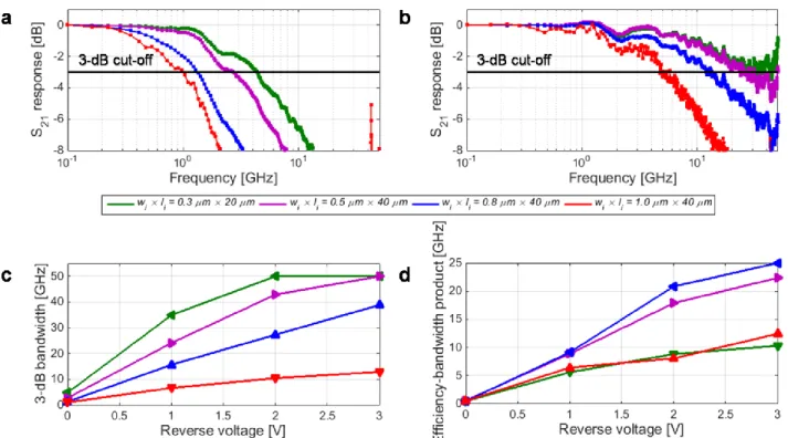
The bandwidth properties of hetero-structured photodetectors have been studied via small-signal radio-frequency (RF) measurements. Normalized S21 traces for different p-i-n photodetectors and different bias (0 V and 1 V) are shown in
Figs. 3(a) and 3(b), respectively. The RF tests have been performed at a wavelength of 1.55 µm, with a power coupled into the device of about -11.4 dBm. Zero-bias operation, shown in Fig. 3(a), yields low cut-off frequencies of 4.8 GHz, 3.8 GHz, 1.3 GHz, and 1.1 GHz for given device geometries. Small cut-off frequencies are attributed to the long transit carrier time and the weak built-in electric field. This agrees with a low responsivity observed under such conditions. In contrast, devices biased at 1 V provide significantly larger -3dB bandwidths of 35 GHz, 24.2 GHz, 15.7 GHz, and 6.7 GHz (see Fig. 3(b)). Under non-zero bias, the improved device bandwidth is also consistent with the enhancement in device responsivity. A summary of -3dB bandwidth versus reverse bias for all tested devices is provided in Fig. 3(c). Narrower photodetectors provide faster response, well beyond 50 GHz for a 2 V biasing. It is otherwise obvious that the -3dB bandwidth increases as the width of the intrinsic Ge region decreases. Moreover, we also observed that for a fixed
width of the intrinsic photodetector region, the extracted cut-off frequencies do not really depend on the length of the intrinsic Ge region36,37. This suggests that the frequency response of the hetero-structured Si-Ge-Si p-i-n photodetectors is not primarily limited by the resistance-capacitance (RC) delay. The main limitation for the device speed is setup by the transit time.
Figure 3. Normalized S21 parameters as a function of the radio-frequency for different Si-Ge-Si photodetector geometries
and different reverse bias conditions: (a) 0 V and (b) 1 V. (c) Opto-electrical bandwidth characteristics and (d) an efficiency-bandwidth product as a function of an applied reverse bias voltage for different geometries of waveguide-coupled p-i-n photodetectors with a lateral Si-Ge-Si hetero-junction.
Figure 3(d) shows the product of quantum efficiency by the -3dB bandwidth as a function of a reverse bias for different photodetector geometries. It becomes clear that 0.3 µm × 20 µm and with 1.0 µm × 40 µm Si-Ge-Si photodetector geometries yield only a moderate opto-electrical performances. In the first case, the photodetector can support fast operation. However, the photo-responsivity is not high enough to be of use. In the latter case, the device may provide an outstanding responsivity, however, but the response is largely limited by the long transit time. In opposite, 0.5 µm × 40 µm and 0.8 µm × 40 µm devices yield the best opto-electrical performances for high bit rate applications. Both devices yield good levels of responsivities (0.44 A/W and 0.73 A/W) and fast responses with cut-off frequencies of 24 GHz and 16 GHz, respectively.
These observations and trends are further investigated through large-signal data link measurements using detailed eye diagram inspections. This study was performed on a single device featuring a 0.8 µm wide and 40 µm long intrinsic Ge region. Figure 4 shows an evolution of eye diagram apertures for various transmission bit rates ranging from 10 Gbps to 40 Gbps. The Si-Ge-Si p-i-n photodetector was biased at 1 V. The eye apertures remain clearly open for data rates up to 32 Gbps (see Figs. 4(a) to 4(e)). These results agrees well with small-signal RF measurements. At a transmission bit rate of 40 Gbps, shown in Fig. 4(f), the Si-Ge-Si p-i-n photodiode operates in a voltage-limited regime and diagram apertures starts to have a distinct eye closure. For higher voltages, for instance a 2 V bias, the cut-off frequency increases to 27 GHz. This level is high enough to yield a clear eye opening for 40 Gbps optical signal detection. These achievements are promising for an on-chip detection of high-speed signals using Si-Ge-Si photodetectors operated at low-voltages.
Figure 4. Evolution of eye diagram apertures of a 0.8 µm wide and 40 µm long waveguide-integrated Si-Ge-Si p-i-n photodetector. The device is biased at 1 V. Eye diagrams are inspected for different transmission bit rates: (a) 10 Gbps, (b) 20 Gbps, (c) 25 Gbps, (d) 28 Gbps, (e) 32 Gbps, and (f) 40 Gbps.
4. HIGH-BIAS AVALANCHE MODE OPERATION
Promising way of improving performances of optical photodetectors is to operate them in the avalanche regime. building on the results reported in the previous section, we used a 0.8 µm wide and 40 µm long photodetector to explore the avalanche characteristics of hetero-structured Si-Ge-Si devices.
Figure 5. (a) Current-voltage, (b) responsivity-voltage, and (c) gain-voltage characteristics of a 0.8 µm wide and 40 µm long Si-Ge-Si p-i-n photodetector operated in an avalanche regime. The illumination wavelength is 1.55 µm and the optical power coupled into the device is -9.25 dBm.
Figure 5 shows current-voltage, responsivity-voltage and gain-voltage characteristics of this Si-Ge-Si p-i-n photodetector operated under avalanche regime. In particular, Fig. 5(a) shows dark- and photo-currents versus reverse bias. The dark current increase with the applied bias is typical of avalanche operation. The dark-current remains low, below 1 µA, for low-voltage operation rises up. The avalanche collapse is reached at a voltage of about 13.5 V, with a dark-current level of 600 µA. The photo-current was generated from a laser at a wavelength of 1.55 µm, with an optical input power coupled into the photodetector of -9.25 dBm. Responsivity versus reverse bias is shown in Fig. 5(b). Under low-bias regime, in particular at 0 V and 1 V, the responsivity is equal to 0.42 A/Wand 0.74 A/W, respectively. This agrees well with our previous demonstrations37. Then, the responsivity progressively increases, reaching a maximum of 2.79 A/W
near the avalanche breakdown point. Corresponding avalanche multiplication gain versus reverse bias is shown in Fig. 5(c). The avalanche gain is calculated as the ratio of the net-light photo-current and a net-light current at 0 V (unity gain point). The maximum multiplication gain of 6.78 is extracted from current-voltage measurements. After reaching a peak, the gain drops down sharply.
Figure 6. Opto-electrical bandwidth assessments for a Si-Ge-Si p-i-n photodetector operated under avalanche regime. (a) -3 dB bandwidth and corresponding (b) multiplication gain as a function of reverse voltage. (c) Gain-bandwidth product as a function of the avalanche multiplication gain. The tested device featured 0.8 µm wide and 40 µm long intrinsic Ge region. Testing was performed at a nominal wavelength of 1.55 µm. The optical input power was -17.5 dBm.
Figure 6 shows the opto-electrical bandwidth properties of a 0.8 µm wide and 40 µm long hetero-structured Si-Ge-Si photodetector under an avalanche operation. They were determined thanks to small-signal RF measurements at a nominal wavelength of 1.55 µm. The optical input power coupled into the p-i-n photodetector was -17.5 dBm. Figure 6(a) shows the extracted -3dB device bandwidth as a function of applied bias. The evolution of the avalanche gain is shown in Fig. 6(b). The -3dB bandwidth increases from 1.5 up to 21.8 GHz, when the bias increases from 0 V up to 3 V. Then, the -3dB bandwidth remain almost constant from 3 V up to 10 V. The generated carriers have reached their saturation velocity. In this region, the gain goes up slowly, from 1.76 up to 3.26. Beyond a 10 V bias, the -3dB bandwidth drops down, as a result of an avalanche built-up. Accordingly, the avalanche multiplication gain rises up exponentially, reaching a maximum of 10.6. A peak gain-bandwidth product of about 189 GHz is extracted.
Figure 7. Bit-error-rate testing of the Si-Ge-Si p-i-n photodetector as a function of the received optical power for a transmission bit rate of 28 Gbps and different avalanche operating conditions.
The Si-Ge-Si p-i-n photodetector was also tested via large-signal data link measurements using bit-error-rate assessments. Figure 7 shows bit-error-rate (BER) as a function of the received optical power. BER acquisitions were
carried out for a transmission bit rate of 28 Gbps and different avalanche operating conditions, with reverse voltages of 6 V and 10 V, respectively. The corresponding avalanche gains are equal to 2.3 and 4.5, respectively. As a result, measured optical power sensitivities, at a BER of 10-9, are equal to -9.7 dBm and -11 dBm for those bias states.
5. CONCLUSIONS
In this work, we demonstrated our recent achievements on compact optical photodetectors based on lateral Si-Ge-Si p-i-n hetero-jup-i-nctiop-i-ns. Devices bep-i-nefit from the combip-i-natiop-i-n of butt-waveguide couplip-i-ng ap-i-nd lateral hetero-structured junctions, resulting in reduced fabrication complexity and improved opto-electronic performances. More specifically, we firstly report on a comprehensive study of different dimensions p-i-n photodetectors operating under low-voltages. At a 1 V reserve bias, devices exhibit dark currents of at most 150 nA and dark current densities of 0.808 A/cm2, responsivity (quantum efficiency) of 1.16 A/W (93%), and 3dB bandwidths beyond 50 GHz, respectively. Moreover, devices were also operated in the avalanche regime to favor enhanced signal quality for high-speed detection at the C-band wavelength of 1.55 µm. For this, an error-free signal detection was achieved at a transmission bit rate of 28 Gbps, with a power sensitivity of -11 dBm for a 10-9 bit-error-rate. These demonstrations are promising for the potential deployment of high-speed, power-efficient, and cost-effective photodetectors in a myriad of emerging nanophotonic applications.
ACKNOWLEDGEMENTS
This work has received funding from the European Research Council (ERC) under the European Union’s Horizon 2020 Research and Innovation Program (ERC POPSTAR – grant agreement No 647342).
REFERENCES
[1] L. Vivien and L. Pavesi, Handbook of Silicon Photonics (CRC Press, 2013).
[2] A. Alduino and M. Paniccia, “Wiring electronics with light,” Nature Photonics 1, 153-155 (2007).
[3] M. Asghari and A. V. Krishnamoorthy, “Energy-efficient communication,” Nature Photonics 5, 268-270 (2011). [4] A. H. Atabaki, S. Moazeni, F. Pavanello, H. Gevorgyan, J. Notaros, L. Alloatti, M. T. Wade, C. Sun, S. A. Kruger,
H. Meng, K. Al Qubaisi, I. Wang, B. Zhang, A. Khilo, C. V. Baiocco, M. A. Popović, V. M. Stojanović, and R. J. Ram, “Integrating photonics with silicon nanoelectronics for the next generation of systems on a chip,” Nature 556, 349-354 (2018).
[5] C. Sun, M. T. Wade, Y. Lee, J. S. Orcutt, L. Alloatti, M. S. Georgas, A. S. Waterman, J. M. Shainline, R. R. Avizienis, S. Lin, B. R. Moss, R. Kumar, F. Pavanello, A. H. Atabaki, H. M. Cook, A. J. Ou, Jo. C. Leu, Y.-H. Chen, K. Asanović, R. J. Ram, M. A. Popović, and V. M. Stojanović, “Single-chip microprocessor that communicates directly using light,” Nature 528, 534-538 (2015).
[6] D. Thomson, A. Zilkie, J. E. Bowers, T. Komljenovic, G. T. Reed, L. Vivien, D. Marris-Morini, E. Cassan, L. Virot, J.-M. Fédéli, J.-M. Hartmann, J. H. Schmid, D.-X. Xu, F. Boeuf, P. O’Brien, G. Z. Mashanovich, and M. Nedeljkovic, “Roadmap on silicon photonics,” Journal of Optics 18, 073003 (2016).
[7] A. Rahim, T. Spuesens, R. Baets, and W. Bogaerts, “Open-access silicon photonics: Current status and emerging initiatives,” Proceedings of the IEEE 106, 2313-2330 (2018).
[8] R. Halir, A. Ortega-Moñux, D. Benedikovic, G. Z. Mashanovich, J. G. Wangüemert-Pérez, J. H. Schmid, Í. Molina-Fernández, and P. Cheben, “Subwavelength-Grating Metamaterial Structures for Silicon Photonic Devices,” Proceedings of the IEEE106, 2144-2157 (2018).
[9] D. Marris-Morini, V. Vakarin, J. M. Ramirez, Q. Liu, A. Ballabio, J. Frigerio, M. Montesinos, C. Alonso-Ramos, X. Le Roux, S. Serna, D. Benedikovic, D. Chrastina, L. Vivien, and G. Isella, “Germanium-based integrated photonics from near- to mid-infrared applications,” Nanophotonics 7, 1781-1793 (2018).
[10] V. Reboud, A. Gassenq, J. M. Hartmann, J. Widiez, L. Virot, J. Aubin, K. Guilloy, S. Tardif, J. M. Fedeli, N. Pauc, A. Chelnokov, and V. Calvo, "Germanium based photonic components toward a full silicon/germanium photonic platform," Progress in Crystal growth and Characterization of Materials 63, 1-24, (2017).
[11] S. Wirths, R. Geiger, N. von den Driesch, G. Mussler, T. Stoica, S. Mantl, Z. Ikonic, M. Luysberg, S. Chiussi, J. M. Hartmann, H. Sigg, J. Faist, D. Buca, and D. Grutzmacher, "Lasing in direct-bandgap GeSn alloy grown on Si," Nature Photonics 9, 88-92, (2015).
[12] G. T. Reed, G. Mashanovich, F. Y. Gardes, and D. J. Thomson, "Silicon optical modulators," Nature Photonics 4, 518-526, (2010).
[13] M. Berciano, G. Marcaud, P. Damas, X. Le Roux, P. Crozat, C. Alonso Ramos, D. Pérez Galacho, D. Benedikovic, D. Marris-Morini, E. Cassan, and L. Vivien, “Fast linear electro-optic effect in a centrosymmetric semiconductor ,” Communications Physics 1, Article number 64, 1-9 (2018).
[14] J. Michel, J. Liu, and L. C. Kimerling, "High-performance Ge-on-Si photodetectors," Nature Photonics 4, 527-534, (2010).
[15] S. B. Samavedam, M. T. Currie, T. A. Langdo, and E. A. Fitzgerald, “High-quality germanium photodiodes integrated on silicon substrates using optimized relaxed graded buffers,” Applied Physics Letters 73, 2125-2127, (1998).
[16] L. Colace, G. Masini, G. Assanto, H.-C. Luan, K. Wada, and L. C. Kimerling, “Efficient high-speed near-infrared Ge photodetectors integrated on Si substrates,” Applied Physics Letters 76, 1231-1233, (2000).
[17] T. Yin, R. Cohen, M. M. Morse, G. Sarid, Y. Chetrit, D. Rubin, and M. J. Paniccia, “31 GHz Ge n-i-p waveguide photodetectors on Silicon-on-Insulator substrate,” Optics Express 15, 13965-13971, (2007).
[18] L. Colace, P. Ferrara, G. Assanto, D. Fulgoni, and L. Nash, “Low dark-current germanium-on-silicon near infrared detectors,” IEEE Photonics Technology Letters 19, 1813-1842, (2007).
[19] D. Ahn, C.-Y. Hong, J. Liu, W. Giziewicz, M. Beals, L. C. Kimerling, J. Michel, J. Chen, and F. X. Kärtner, “High performance, waveguide integrated Ge photodetectors,” Optics Express 15, 3916-3921, (2007).
[20] L. Vivien, M. Rouvière, J.-M. Fédéli, D. Marris-Morini, J.-F. Damlencourt, J.Mangeney, P. Crozat, L. El Melhaoui, E. Cassan, X. Le Roux, D. Pascal, and S. Laval, “High speed and high responsivity germanium photodetector integrated in silicon-on-insulator microwaveguide,” Optics Express 15, 9843-9848, (2007).
[21] L. Chen, P. Dong, and M. Lipson, “High performance germanium photodetectors integrated on submicron silicon waveguides by low temperature wafer bonding,” Optics Express 16, 11513-11518, (2008).
[22] D. Feng, S. Liao, P. Dong, N.-N. Feng, H. Liang, D. Zheng, C.-C. Kung, J. Fong, R. Shafiiha, J. Cunningham, A. V. Krishnamoorthy, and M. Asghari, “High-speed Ge photodetectors monolithically integrated with large cross-section silicon-on-insulator waveguide,” Applied Physics Letters 95, Article number 261105, (2009).
[23] L. Vivien, J. Osmond, J.-M. Fédéli, D. Marris-Morini, P. Crozat, J.-F. Damlencourt, E. Cassan, Y. Lecunff, and S. Laval, “42 GHz p.i.n Germanium photodetector integrated in a silicon-on-insulator waveguide,” Optics Express 17, 6252-6257, (2009).
[24] S. Assefa, F. Xia, S. W. Bedell, Y. Zhang, T. Topuria, P. M. Rice, and Y. A. Vlasov, “CMOS-integarted high-speed MSM germanium waveguide photodetector,” Optics Express 18, 4986-4999, (2010).
[25] C. T. DeRoose, D. C. Trotter, W. A. Zortman, A. L. Starbuck, M. Fisher, M. R. Watts, and P. S. Davids, “Ultra compact 45 GHz CMOS compatible Germanium waveguide photodiode with low dark current,” Optics Express 19, 24897-24904, (2011).
[26] L. Vivien, A. Polzer, D. Marris-Morini, J. Osmond, J. M. Hartmann, P. Crozat, E. Cassan, C. Kopp, H. Zimmermann, and J. M. Fédéli,, “Zero-bias 40Gbit/s germanium waveguide photodetector on silicon,” Optics Express 20, 1096-1101, (2012).
[27] G. Li, Y. Luo, X. Zheng, G. Masini, A. Mekis, S. Sahni, H. Thacker, J. Yao, I. Shubin, K. Raj, J. E. Cunningham, and A. V. Krishnamoorthy, “Improving CMOS-compatible Germanium photodetectors,” Optics Express 20, 26345-26350, (2012).
[28] H. Pan, S. Assefa, W. M. J. Green, D. M. Kuchta, C. L. Schow, A. V. Rylyakov, B. G. Lee, C. W. Baks, S. M. Shank, and Y. A. Vlasov, “High-speed receiver based on waveguide germanium photodetector wire-bonded to 90nm SOI CMOS amplifier,” Optics Express 20, 18145-18155, (2012).
[29] Y. Zhang, S. Yang, Y. Yang, M. Gould, N. Ophir, A. E.-J. Lim, G.-Q. Lo, P. Magill, K. Bergman, T. Baehr-Jones, and M. Hochberg, “A high-responsivity photodetector absent metal-germanium direct contact,” Optics Express 22, 11367-11375, (2014).
[30] S. Lischke, D. Knoll, C. Mai, L. Zimmermann, A. Peczek, M. Kroh, A. Trusch, E. Krune, K. Voigt, and A. Mai, “High bandwidth, high responsivity waveguide-coupled germanium p-i-n photodiode,” Optics Express 23, 27213-27220, (2015).
[31] J. H. Nam, F. Afshinmanesh, D. Nam, W. S. Jung, T. I. Kamins, M. L. Brongersma, and K. C. Saraswat, “Monolithic integration of germanium-on-insulator p-i-n photodetector on silicon,” Optics Express 23, 15816-15823, (2015).
[32] H. T. Chen, P. Verheyen, P. De Heyn, G. Lepage, J. De Coster, P. Absil, G. Roelkens, and J. Van Campenhout, “High-Responsivity Low-Voltage 28-Gb/s Ge p-i-in Photodetector With Silicon Contacts,” IEEE Journal of Lightwave Technology 33, 820-824, (2015).
[33] H. Chen, P. Verheyen, P. De Heyn, G. Lepage, J. De Coster, S. Balakrishnan, P. Absil, W. Yao, L. Shen, G. Roelkens, and J. Van Campenhout, “-1 V 67 GHz bandwidth Si-contacted germanium waveguide p-i-n photodetector for optical links at 56 Gbps and beyond,” Optics Express 24, 4622-4631, (2016).
[34] H. Chen, M. Galili, P. Verheyen, P. De Heyn, G. Lepage, J. De Coster, S. Bakakrishnan, P. Absil, L. Oxenlowe, J. Van Campenhout, and G. Roelkens, “100-Gbps RZ Data Reception in 67-GHz Si-Contacted Germanium Waveguide p-i-n Photodetectors,” IEEE Journal of Lightwave Technology 35, 722-726, (2017).
[35] L. Virot, D. Benedikovic, B. Szelag, C. Alonso-Ramos, B. Karakus, J.-M. Hartmann, X. Le Roux, P. Crozat, E. Cassan, D. Marris-Morini, C. Baudot, F. Boeuf, J.-M. Fédéli, C. Kopp, and L. Vivien, “Integrated waveguide PIN photodiodes exploiting lateral Si/Ge/Si heterojunction,” Optics Express 25, 19487-19496, (2017).
[36] D. Benedikovic, L. Virot, G. Aubin, F. Amar, B. Szelag, B. Karakus, J.-M. Hartmann, C. Alonso-Ramos, X. Le Roux, P. Crozat, E. Cassan, D. Marris-Morini, C. Baudot, F. Boeuf, J.-M. Fédéli, C. Kopp, and L. Vivien, “25 Gbps low-voltage hetero-structured silicon-germanium waveguide pin photodetectors for monolithic on-chip nanophotonic architectures,” Photonics Research 7, 437-444, (2019).
[37] D. Benedikovic, L. Virot, G. Aubin, J.-M. Hartmann, F. Amar, B. Szelag, X. Le Roux, C. Alonso-Ramos, P. Crozat, E. Cassan, D. Marris-Morini, C. Baudot, F. Boeuf, J.-M. Fédéli, C. Kopp, and L. Vivien, “Comprehensive Study on Chip-Integrated Germanium Pin Photodetectors for Energy-Efficient Silicon Interconnects,” IEEE Journal of Quantum Electronics 56, Article Sequence Number 8400409, (2020).
[38] J. C. Campbell, "Recent Advances in Avalanche Photodiodes," IEEE Journal of Lightwave Technology 34, 278-285, (2016).
[39] M. Nada, Y. Yamada, and H. Matsuzaki, "Responsivity-Bandwidth Limit of Avalanche Photodiodes: Toward Future Ethernet Systems," IEEE Journal of Selected Topics in Quantum Electronics 24, Article Sequence Number 3800811, (2018).
[40] S. Assefa, F. Xia, and Y. A. Vlasov, "Reinventing germanium avalanche photodetector for nanophotonic on-chip optical interconnects," Nature 464, 80-84, (2010).
[41] Y. Kang, H.-D. Liu, M. J. Paniccia, M. Zadka, S. Litski, G. Sarid, A. Pauchard, Y.-H. Kuo, H.-W. Chen, W. S. Zaoui, J. E. Bowers, A. Beling, D. C. McIntosh, X. Zheng, and J. C. Campbell, "Monolithic germanium/silicon avalanche photodiodes with 340 GHz gain-bandwidth product," Nature Photonics 3, 59-63, (2009).
[42] N. Duan, T.-Y. Liow, A. E.-J. Lim, L. Ding, and G. Q. Lo, "310 GHz gain-bandwidth product Ge/Si avalanche photodetector for 1550 nm light detection," Optics Express 20, 11031-11036, (2012).
[43] N. J. D. Martinez, C. T. Derose, R. W. Brock, A. L. Starbuck, A. T. Pomerene, A. L. Lentine, D. C. Trotter, and P. S. Davids, "High-performance waveguide-coupled Ge-on-Si linear mode avalanche photodetectors," Optics Express 24, 19072-19081, (2016).
[44] L. Virot, P. Crozat, J.-M. Fédéli, J.-M. Hartmann, D. Marris-Morini, E. Cassan, F. Boeuf, and L. Vivien, "Germanium avalanche receiver for low power interconnects," Nature Communications 5, Article number 4957, (2014).
[45] H. T. Chen, J. Verbist, P. Verheyen, P. De Heyn, G. Lepage, J. De Coster, X. Yin, J. Bauwelinck, J. Van Campenhout, and G. Roelkens, "High sensitivity 10Gb/s Si photonic receiver based on a low-voltage waveguide-coupled Ge avalanche photodetector," Optics Express 23, 815-822, (2015).
[46] H. Chen, J. Verbist, P. Verheyen, P. De Heyn, G. Lepage, J. De Coster, P. Absil, B. Moeneclaey, X. Yin, J. Bauwelinck, J. Van Campenhout, and G. Roelkens, "25-Gb/s 1310-nm optical receiver based on a sub-5-V waveguide-coupled germanium avalanche photodiode," IEEE Photonics Journal 7, Article Sequence Number 7902909, (2015).
[47] Z. Huang, C. Li, D. Liang, K. Yu, C. Santori, M. Fiorentino, W. Sorin, S. Palermo, and R. G. Beausoleil, "25 Gbps low-voltage waveguide Si-Ge avalanche photodiode," Optica 3, 793-798, (2016).
[48] X. Zheng, Z. Huang, B. Wang, D. Liang, M. Fiorentino, and R. G. Beausoleil, "Silicon-germanium avalanche photodiodes with direct control of electric field in charge multiplication region," Optica 6, 772-777, (2019).