HAL Id: tel-00815762
https://tel.archives-ouvertes.fr/tel-00815762
Submitted on 19 Apr 2013HAL is a multi-disciplinary open access archive for the deposit and dissemination of sci-entific research documents, whether they are pub-lished or not. The documents may come from teaching and research institutions in France or abroad, or from public or private research centers.
L’archive ouverte pluridisciplinaire HAL, est destinée au dépôt et à la diffusion de documents scientifiques de niveau recherche, publiés ou non, émanant des établissements d’enseignement et de recherche français ou étrangers, des laboratoires publics ou privés.
domain wall dynamics in FePt and NiFe nanostructures
van Dai Nguyen
To cite this version:
van Dai Nguyen. Magnon magnetoresistance, magnetization reversal and domain wall dynamics in FePt and NiFe nanostructures. Materials Science [cond-mat.mtrl-sci]. Université de Grenoble, 2012. English. �tel-00815762�
THÈSE
Pour obtenir le grade de
DOCTEUR DE L’UNIVERSITÉ DE GRENOBLE
Spécialité : NANOPHYSIQUE Arrêté ministériel :
Présentée par
Văn Đại NGUYỄN
Thèse dirigée par Dr. Alain MARTY
codirigée par Dr. Jean-Philippe ATTANÉ et Laurent VILA préparée au sein du Laboratoire de Nanostructures et
Magnétisme et de l'École Doctorale de Physique
Magnon magnetoresistance, magnetization
reversal and domain wall dynamics in FePt and
NiFe nanostructures
Thèse soutenue publiquement le: 28 September 2012
Devant le jury composé de:
Monsieur Hervé COURTOIS
Professeur, UJF Grenoble, Président
Monsieur André THIAVILLE
Directeur de recherche, Paris XI Orsay, Rapporteur
Monsieur Matthieu BAILLEUL
Directeur de recherche, IPCMS Strasbourg, Rapporteur
Monsieur Dafiné RAVELOSONA
Directeur de recherche, IEF Orsay, Examinateur
Monsieur Alain MARTY
Directeur de recherche, CEA Grenoble, Directeur de thèse
Monsieur Jean-Philippe ATTANÉ
Contents
Introduction 5
1 Domain wall and magnetoresistance in nanostructures 11
1.1 Magnetic domain wall in nanowires . . . 11
1.2 Domain wall motion in magnetic nanostructures . . . 14
1.2.1 Field induced domain wall motion . . . 15
1.2.1.1 Landau-Lifschitz-Gilbert (LLG) equation . . . 15
1.2.1.2 Different regime of domain wall motion without pinning in ideal nanowires . . . 15
1.2.1.3 Different regime of domain wall motion in nanowires: The role of intrinsic defects . . . 17
1.2.2 Current induced domain wall motion . . . 19
1.2.2.1 Early model of current induced domain wall motion . . . 19
1.2.2.2 Model of current induced domain wall motion . . . 19
1.2.2.3 Effect of Oersted field and Joule heating on current induced domain wall motion . . . 20
1.2.3 Applications of current induced domain wall motion . . . 21
1.3 Magnetoresistance effects in nanostructures: Domain wall detection . . . 22
1.3.1 Anisotropic magnetoresistance . . . 22
1.3.2 Extraordinary Hall effect . . . 24
1.3.3 Giant magnetoresistance . . . 25
1.4 Conclusions . . . 28
2 Magnetization reversal in FePt based thin films and nanowires 29 2.1 FePt based thin films . . . 29
2.1.1 Growth of a single FePt thin film on MgO substrate . . . 29
2.1.2 Magnetization reversal of a single FePt thin film . . . 31
2.1.3 FePt based spin valve thin film on MgO substrate . . . 34
2.2.1 Effect of magnetic dendrite width on the magnetization reversal mode
of FePt nanowires . . . 37
2.2.2 Enhancement of coercive field in FePt nanowires . . . 41
2.2.2.1 Experimental observation of coercivity enhancement in FePt nanowires . . . 41
2.2.2.2 Modeling the enhancement of the coercivity in FePt nanowire 42 2.2.2.3 Contribution of the mean edge roughness to the coercivity . 44 2.2.2.4 Effect of nucleation distance on the magnetization reversal modes in narrow FePt nanowires . . . 45
3 Detection of magnetization reversal in FePt nanowires using Magnon mag-netoresistance 49 3.1 Observation of Magnon magnetoresistance in FePt thin films . . . 49
3.2 Detection of magnetization reversal and domain wall position in FePt nanowires 53 3.2.1 Detection of magnetization switching in FePt nanowires . . . 53
3.2.2 Measurement of domain wall position and motion along FePt nanowires 56 3.3 Hall contribution to the MMR measurement . . . 59
3.3.1 Introduction . . . 59
3.3.2 Asymmetric signal in longitudinal MMR measurement . . . 60
3.3.3 Model of Hall contribution to MMR measurement . . . 62
4 Magnon magnetoresistance in NiFe nanowires and nanomagnets 67 4.1 Observation of the Magnon magnetoresistance in NiFe nanowires . . . 68
4.2 Detection of magnetization reversal and domain wall position in NiFe nanowires 71 4.2.1 Detection of magnetization reversal in NiFe nanowires . . . 71
4.2.2 Measurement of domain wall position along a NiFe nanowire . . . 72
4.3 Detection of magnetization reversal of a single nanomagnet . . . 75
4.4 Enhancement of MMR signal . . . 80
5 Stochasticity of domain wall depinning in ferromagnetic nanowires 83 5.1 State of the art of field and current induced domain wall depinning . . . 83
5.1.1 Stochasticity of domain wall depinning under applied field . . . 83
5.1.2 Domain wall depinning under applied current . . . 85
5.2 Studying field and current induced domain wall depinning in FePt and NiFe nanowires . . . 89
5.2.1 Detection of domain wall depinning using transport measurements . . . 89
5.2.2 Simple path . . . 91
CONTENTS
5.2.4 Alternative paths . . . 95
5.2.5 Effect of applied current on domain wall depinning in FePt and NiFe nanowires . . . 98
5.2.6 Effect of the constrictions on domain wall depinning . . . 99
Conclusions and perspectives 103 A Sample preparation 107 A.1 FePt thin films deposition . . . 107
A.1.1 Description of the Molecular Beam Epitaxy system . . . 107
A.1.2 FePt deposition process . . . 108
A.2 Nanostructures fabrication . . . 109
A.2.1 Optical lithography . . . 109
A.2.2 E-beam lithography . . . 110
B Angular dependence of MMR measurements 113
C Further analysis of domain wall depinning by serial paths 117
Bibliography 118
List of publication 131
Introduction
Spintronics
The discovery of the giant magnetoresistance (GMR) [1, 2] which awarded the 2007 Nobel Prize in Physics to A. Fert and P. Grünberg has triggered the rise of a new field of electronics called spintronics. This discovery is associated to a remarkable transition from fundamental research of spin-dependent transport in nanostructures to device applications in the area of data storage technologies. Spintronics devices exploit the spin degree freedom of electron rather than its charge, and offers new ways to store, carry and control the information. Such devices could also combine several advantages such as non-volatility, high speed data processing, reduced power consumption and high integration densities [3].
Among other, research in spintronics address two basic requirements: the detection and the manipulation of the magnetization in ferromagnetic nanostructures, which are the basic building blocks of spintronics. These two points are major challenges for fundamental research and the main topics of this thesis.
Magnetization reversal detection
Magnetoresistance (MR) effects based on spin-dependent transport properties can provide simple and fast ways to detect magnetization reversal in nanostructures. So far, the develop-ment of spintronics is based on few magnetoresistances including the giant magnetoresistance (GMR), the tunneling magnetoresistance (TMR), the anisotropic magnetoresistance (AMR) and the extraordinary Hall effect (EHE).
Important for both fundamental research and applications, the GMR is based on the large change of the resistance of a magnetic multilayer under the application of a magnetic field. The discovery of the GMR is considered to be the starting point of spintronics. Shortly later, spin-valve structures composed of two ferromagnetic layer separated by a nonmagnetic metallic layer, and exhibiting GMR effect were developed [4]. Basically, GMR spin-valves structures reveal the change in resistance depending on the relative orientation of magnetization of the two ferromagnetic layers in which the resistance is low when the magnetization in ferromagnetic layers are parallel and high when anti-parallel.
Later, the observation of room temperature TMR in 1995 [5] in magnetic tunnel junctions (MTJs) [6] was considered as a second breakthrough in the development of spintronics. MTJs consist of two ferromagnetic layers separated by an ultra-thin insulating layer in which the electrons can tunnel from one ferromagnetic layer to the other. As for GMR, the resistance of the stack depends on the relative orientation of the magnetization of the ferromagnetic layers. GMR reaches up to 180 % values whereas TMR goes up to 1000 % in MgO-based MTJ.
GMR and MTJ are the basic elements of spintronics devices which include magnetic field sensors, hard drives, read heads and magnetoresistive random access memory (MRAM) [7]. The higher the MR signal is, the smaller and faster the storage element can be.
Apart from the great potential for application, GMR and TMR are also of great interest for studying novel spintronics nanostructures since the change of resistance is quantitatively proportional to the orientation of the magnetization. Indeed, GMR measurement has been used to study magnetization reversal in an individual nanomagnet such as nanopillar [8] and is particularly used to detect domain wall (DW) position and motion in nanowires [9].
Although it was replaced by GMR for magnetoresistive HDD read heads [7], AMR is still an extremely important tool for studying the magnetic state of nanostructures. AMR was first observed in 1856 by William Thomson [10] and arises from the spin orbit coupling. The amplitude of AMR is much smaller than GMR and TMR (a few percent in some alloys based on 3d metals) but the resistance value is directly related to the orientation of the magnetization and the current lines [11]. AMR measurements have been thus extensively used to study magnetization reversal in materials with in-plane magnetization [11, 12, 13] and have been used more recently to probe the presence of DW in nanowires [14] or to distinguish different type of DW [15].
The EHE arises also from the spin–orbit scattering. The possibility for applications, such as magnetic sensors and nonvolatile MRAM, has been mentioned but no significant progress has reported until recently [16]. For nanostructures with perpendicular magnetization, the EHE is the most common detection technique of magnetization reversal [17]. Additionally, EHE is very important for characterizing DW motion and precise detection of DW position within Hall crosses [18].
It is worth noticing that extensive approach to follow DW motion is the use of imaging techniques such as Kerr, magnetic force microscopy (MFM), Lorentz transmission electron microscopy techniques and so on. In this thesis, we will mostly focus on the ways using magnetotransport measurements.
Magnetization reversal manipulation
The second important requirement for further development of spintronics is the ability to manipulate the magnetization reversal in nanostructures, which has been done conventionally
using magnetic field. In the first generation of MRAM devices, the magnetization of the memory element is switched by local magnetic fields generated when passing current through nearby metallic wires [19]. However, the writing current is high and limited by the CMOS electronic circuit.
For that reason, more efficient ways to switch the magnetization of nanodevices without the use of magnetic fields are sought. For instance, laser induced magnetization switching provide an ultra-fast way to manipulate magnetization [20] which can offer new perspectives for applications.
Recently, the experimental demonstration of current induced DW motion and magneti-zation switching in magnetic nanostructures opened a fast and promising way to manipulate magnetization.
Due to the spin dependent scattering of the electrons in magnetic materials, the electrical current is spin polarized, the direction of the spins being aligned with the direction of the local magnetic moments. The first concept of spin transfer torque induced DW motion was proposed by Berger in 1984 [21]. The idea is that across a DW, the exchange interaction aligns the spin direction of the conduction electron with the direction of local magnetization. To conserve the total angular momentum, it has to be transferred to the local magnetization, which is equivalent to a torque acting on the magnetization. This interaction consequently induces a displacement of the DW in the direction of the electron flow.
Experimental studies on current-induced DW motion have been performed shortly after the theoretical prediction (cf. ref. [22]). However, these early experiments have been mostly studied on thick NiFe films in which several difficulties arise as the extended thin films can result in more complex DW structures. Also, heating and Oersted fields become significant when increasing the film thickness and the current intensity. Importantly, these pioneering studies established the first steps for investigating current-induced DW motion.
The second concept of spin-transfer torque was proposed by Slonczewski in 1996 [23] and predicted that a flow of spin polarized current can exert a torque on the magnetic moments of thin magnetic layers and consequently switch the magnetization. Shortly later, this prediction was experimentally confirmed using point contact geometries [24] and nanopillars [25]. These results have basically shown that in order to observe the spin transfer torque effect, one needs to avoid the effect of the Oersted field and heating by reducing the size of the sample to nanoscale. Thus nanostructures such as nanopillar and nanowires became ideal systems for studying current-induced magnetization switching and DW motion.
Thanks to recent advances in lithographic techniques, magnetic nanostructures with lateral dimensions as small as a few tens of nanometers can be realized. In such nanostructures, the magnetic configuration can be properly tuned. For instance it is possible to study the current induced motion of a single DW inside nanowires, or the magnetization switching in the
macro-spin limit in pillars. Consequently, the topic of current induced magnetization switching became very active, both for experiments and theories [26]. This phenomenon offers an alternative way to conventional field-induced DW motion and new concepts based on DW motion such as the race-track memory or DW logic devices emerged [27]. These devices could simplify the design, integration and down-scaling of device architecture altogether with faster data processing and lower power consumption capabilities.
In the last decade, the number of studies on current induced DWs in magnetic nanowires has boomed. At first, single permalloy (NiFe) nanowires [28] or NiFe based spin valve structures [29] have been used to perform such experiments. As NiFe is the softest magnetic material, the magnetic properties can be well controlled, DW velocities are high (~100 m/s) [30] and the spin torque was expected to be efficient. Nevertheless, the critical current density for DW displacement at zero field is high ∼ 1012 A/m2 [26].
More recently, this topic progressively moved toward systems with perpendicular magneti-zation as CoPt [31], Co/Ni [32] and FePt [33] nanowires. These systems with high anisotropy increase the thermal stability and exhibit narrow DW that should present higher spin torque efficiencies (through the large magnetic gradient) and device densities [26].
On the theoretical side, the studies on current induced DW motion also flourished. Basi-cally, the idea is to extend the Landau-Lifshitz-Gilbert (LLG) equations by adding spin transfer torque terms, i.e., adiabatic and non adiabatic spin torque terms [34]. However, no consensus has still emerged on the origin and magnitude of the non adiabatic term. Moreover additional contributions such as Oersted field [35], Rashba effect [31] or automotive force [36] complicate the precise understanding of the phenomena.
Although such promising devices based on current induced DW motion motivated a large effort of research but several important open question need to be addressed. Discrepancies between theoretical and experimental results which linked to the nature of the current induced torques, the origin, the amplitude or even the existence of the non adiabatic torque term still exist. Different measurement methods and analysis has been used, which induce obviously different conclusions [26]. Additionally, the reduction of current densities for lower power consumption and increase of DW velocities for fast data processing are also major challenges. Also, another promising way to manipulate the magnetization reversal in nanostructures is the use of pure spin currents which are created by either spin accumulation at the inter-face between ferromagnetic and metallic materials [37] or by the spin Hall effect [38]. The generation and detection of pure spin currents which are usually based on lateral spin valve structures [39] are also interesting perspectives in this field.
To conclude, the detection and the manipulation of magnetization reversal in nanostruc-tures are crucial issues for both fundamental research and practical applications of spintronics devices. In this context, this PhD thesis will used a novel magnetoresistance effect, i.e., the
Magnon magnetoresistance (MMR), to detect the magnetization reversal in nanostructures. We will show that this MR is able to provide information such as the DW position during the magnetization reversal. We will emphasis the versatility of this technique by doing so for two typical magnetic systems with planar (NiFe) and perpendicular magnetization (FePt). Having detected the position of DW in nanowires, we will study the DW depinning mechanism from different class of pining sites, either by field or current. For any device based on DW, this effect must be controlled precisely. We will show that similar features are found for both materials and a microscopic description of the phenomena will be given altogether with the comparison of field and current effects.
This thesis is organized as follows:
Chapter 1: Domain wall and magnetoresistance in nanostructures This chapter
de-scribes the micromagnetic origin of DW formation and the basic model of DW dynamics in nanostructures. The magnetotransport measurements which are usually used to detect mag-netization reversal and characterize the DW motion in nanostructures are also presented.
Chapter 2: Magnetization reversal in FePt based thin films and nanowires
Magne-tization reversal in single layer FePt films and nanowires are presented, emphasizing on the dimensionality effect and the variation of reversal modes when reducing the wire width.
Chapter 3: Detection of magnetization reversal in FePt nanowires using the Magnon magnetoresistance This chapter will give a short description of the MMR in FePt thin film.
We then show that MMR can be used to probe magnetization reversal in FePt nanowires and detect the switching field, the position of DW and its propagation along nanowires.
Chapter 4: Magnon magnetoresistance in NiFe nanowires and nanomagnets We
will show that MMR measurements can be extended to systems with in-plane magnetization, as NiFe nanowires. We highlight the transition of MR signature from AMR to MMR by tuning the shape anisotropy and use the MMR to study the magnetization reversal in NiFe nanowires and nanomagnets.
Chapter 5: Stochasticity of domain wall depinning in ferromagnetic nanowires In
this chapter, we study the stochasticity of DW depinning under applied field and current in magnetic nanowires having perpendicular (FePt) or in plane (NiFe) magnetization. By changing the class of DW pinning site, we observe three different behaviors of DW depinning in both systems and provide the associated microscopic descriptions.
Chapter 1
Domain wall and magnetoresistance in
nanostructures
In this chapter, we begin with a short description of the domain wall (DW) structures in magnetic nanowires. We then discuss the theoretical models which have been developed to describe the phenomenon of the DW motion in nanowires driven by the magnetic field or the spin polarized current. The concepts for data storage applications based on the phenomenon of current induced DW motion will be shortly presented.
Finally, we will describe the experimental techniques to probe the position of a DW in nanowires which is a key point for studying field or current induced DW motion. In particular, we emphasize on the magneto-transport measurements which we mostly used in our studies, as they are well adapted to nanoscale structures.
1.1
Magnetic domain wall in nanowires
Magnetic DWs are boundaries between magnetic domain of different magnetic orientations. DWs play an important role in the magnetization reversal process of magnetic materials and have been intensively studied for many decades [40].
Basically, the formation of a domain results from the competition between various energy terms being: exchange, magnetocrystalline, Zeeman and magnetostatic energies. The total energy of the system is simply the sum of those energy terms:
E = Eex.+ EM C.+ EZeeman+ Emag. (1.1) As for all physical systems, the magnetic system tends to minimize its free energy. Since the magnitude of the magnetization vector is fixed, the way to do so is to vary its direction. The exchange energy (Eex.) is minimized when the orientation of neighboring spins are
par-allel to each other. The magnetocrystalline energy (EM C.) is associated to the direction of the magnetization relative to the some structural axes of the crystal. The Zeeman energy (EZeeman.) is minimized when the orientation of magnetization and the externally applied field are parallel. The magnetostatic energy arising from the dipole–dipole interaction is responsible for the formation of domain structures. Indeed, any uniformly magnetized regions will have lines of M that terminate on its surfaces. These sources and sinks of lines of magnetization will give rise to a nonzero divergence at these points. Using the basic relationship B = µ0(H +M ), we can express the divergence of M as:
∇.M = ∇.B
µ0
− ∇.H (1.2)
since the Maxwell’s equation shows that ∇.B = 0, it leads to ∇.M = −∇.H
Hence these sources and sinks of magnetization at the sample surfaces will give rise to a field H that ensures the continuity of lines of B. This field is known as the demagnetizing field. The energy associated with this stray field H is expressed in the form of two equivalent integrals: Emag. = 1 2µ0 ˆ all space H2dV = −1 2µ0 ˆ sample H.M dV (1.3)
Note that the first expression is always positive, the second thus also must be always positive. The system will try to minimize this energy term as much as possible, making the stray field as small as possible. The second expression can be seen as the energy of a dipole
M dV in the field created by the environment. By forming a non-uniform, flux-closed magnetic
state, it is possible to reduce the number of lines of M that terminate on the sample surfaces and hence reduce the magnetostatic energy [41].
In general, one observes large uniformly magnetized regions separated by the regions where the magnetization rotates from the direction of one domain to the next. This region of non-uniform magnetization is called a DW. There are two typical types of DW known as Bloch and Néel (cf., fig. 1.1). Within a Bloch wall, the magnetization is oriented parallel to the plane of the wall. Whereas, in a Néel wall, the rotation of magnetization is perpendicular to the plane of the wall.
1.1. Magnetic domain wall in nanowires
Figure 1.1: Schematics of (a) Bloch and (b) Néel DWs. In a Bloch wall, the magnetization rotates in a plane parallel to the plane of the wall. In a Néel wall, the magnetization rotates in a plane perpendicular to the wall (Figures are reproduced from [40])
In principle, the competition between the exchange and the magnetic anisotropy is respon-sible for the size of the DWs. If the exchange energy dominates, the wall tends to be wider, it is due to the fact that a small angle between adjacent spins results in a smaller exchange energy. On the contrary, the anisotropy energy causes a narrow DW, inside the wall the direction of spins is away from the easy axis of magnetization.
Figure 1.2: (a) Schematic presenting a magnetic wire with two domains pointing in opposite directions (red and blue arrows) and a domain wall (dotted line) separating the two domains. (b) top view of the spin structure of a transverse DW and (c) a vortex DW (Figures are reproduced from [26]).
In the case of nanowires with an in plane magnetization, the spin structures of DWs arising from the competition between the exchange energy and demagnetizating energy are predicted to be transverse walls or vortex walls (cf., fig. 1.2) which depends on the width and thickness of the nanowires [42]. In the transverse wall, the spins rotate in the plane of the structure. Whereas, in vortex wall, the spins curl around the vortex core where the
magnetization is pointing out of the plane with a polarity pointing up or down. Also, the in-plane magnetization can curl clockwise or counter-clockwise around the vortex core leading to multiple configuration states. The energies of the two wall types vary with the geometry and material and it can be calculated from the micromagnetic simulations [26].
In film with perpendicularly magnetized materials, the anisotropy axis is perpendicular to the film plane and the anisotropy K is much larger than the demagnetizing energy K0 = µ0MS2/2 so that the magnetization is oriented perpendicularly to the film plane. The DW exhibit a Bloch configuration inside the layer and tends to the Néel one close to the surfaces (closure). The Bloch wall width is proportional to 4 = q
A
K where A is exchange constant and K is anisotropy constant. In these systems, DW width parameters,4 are typically of the order of a few nanometers. In FePt epitaxial thin films used in our study, the very strong magnetocrystalline anisotropy induces very narrow Bloch DW (4~1 nm).
1.2
Domain wall motion in magnetic nanostructures
In principle, the operation of DW based devices is based on the displacement of DWs between at least two positions using either applied field or current pulses. Therefore, it is important to understand how DWs pin and depin in a magnetic nanostructure. It has been shown that there are several ways to pin DWs in magnetic nanostructures. For instance, the artificial pinning centers which can be properly defined using lithographies allows one to pin a DW at precise position in a nanowire. In nanowires with in-plane magnetization, there are various designs of artificial pinning sites which are mostly the notches or the constrictions with various widths and depths [42, 43]. For nanowires with out of plane magnetization, the pinning sites can be created using the local geometry of nanowires such as constrictions [44, 33], Hall crosses [45]. It can also be obtained by local change of the layer thickness [46], local decrease of the anisotropy using ion irradiation [47], pinning due to the edge roughness or lithographic defects [48]. Importantly, in such high anisotropic systems, the pinning sites due to intrinsic defects of layers are critical and can also efficiently pin DW [49]. The pinning can be due to a decrease of energy through the change of the DW length or by a reduction of the magnetocrystalline energy in the pinning potential landscape.
Once a DW is pinned, it will leave the pinning sites promptly if the strength of DW driving forces are strong enough to overcome the pinning barrier. Otherwise, they can cross the barrier by thermal activation, but with random delay leading to stochasticity. These DW driving forces can be provided by either an applied magnetic field through the Zeeman energy or by the electrical current through the spin transfer torque. This aspect will be discussed on the frame-work of the theoretical models which have been developed to describe the field and current induced DW motion.
1.2. Domain wall motion in magnetic nanostructures
1.2.1
Field induced domain wall motion
1.2.1.1 Landau-Lifschitz-Gilbert (LLG) equation
Understanding and controlling the field induced motion of DWs in nanowires [43, 50, 51] is an important preliminary step for studying their current-driven dynamics.
The dynamic of the DW motion under the influence of an applied field can be described by Landau-Lifschitz-Gilbert (LLG) equation: ∂m ∂t = −γ− →m ×−−−→H ef f.+ α−→m × ∂−→m ∂t (1.4)
where m is the magnetization normalized to the saturation value, Hef f is the effective field which includes the external magnetic field and the contributions of anisotropy, demagnetizing and exchange fields, γ = gµB/~ is the gyromagnetic ratio where µB is the Bohr magneton, g the Landé factor, and α the Gilbert damping constant. The first term on the right-hand side of equation 1.4 is the precessional term which leads to the precession of the magnetization around the effective field direction. The second term is the damping term leading to the relaxation of magnetization towards this effective field.
1.2.1.2 Different regime of domain wall motion without pinning in ideal nanowires
Schryer and Walker [52] have studied the dynamic of DW motion deriving the first analytical solution for the motion of a Bloch wall in a uniaxial bulk materials under the influence of an applied field. The analytical solution within 1D model have predicted two separated regimes: a steady motion with a high mobility at low field and the precessional regime with a low mobility at high fields.
In an ideal nanowire without pinning sites, the motion of a DW has distinct characteristics depending on the magnitude of the applied field. In the first regime, at low fields, the DW velocity reach a steady value. In this stationary regime, the velocity increases linearly with field, according to the relation [43]:
ν(H) = γ4
α H (1.5)
where ν(H), γ, 4, α, H are velocity of DW motion, gyromagnetic ratio, DW width, Gibert damping, magnetic field, respectively.
Figure 1.3: DW velocity determined by time-resolved MOKE measurements in a single layer permalloy nanowire as function of the applied field. This curve shows two regimes of the DW motion which are separated by the Walker breakdown field. (Figures are reproduced from ref. [53]).
When the field exceeds a certain threshold value, called Walker breakdown field, the average DW velocity drops sharply. Above this field, the DW moves in a complex manner, and its velocity oscillates in time. When the field is increased further, the average velocity is again proportional to the field, although the wall mobility is strongly reduced compared to the low-field value. The velocity in this second regime depends on the low-field value according to the relation:
ν(H) = γ4
α + α−1H (1.6)
There are several experimental results on the dynamic of DW motion in nanowires using time resolved measurements. The parameter widely used to characterize DW motion is the wall mobility which is defined as the change of DW velocity with the applied field. For example, Ono et al., [9] have used GMR measurements to probe the propagation of the DWs in 500 nm wide NiFe/Cu/NiFe multilayer structures. They found that the DW velocity increases linearly with field above a threshold value but with relatively low mobilities, ν/H of about 2.6 m/s.Oe. Atkinson et al., [54] performed a similar study on a single layer Permalloy nanowire us-ing time-resolved MOKE experiments. The DW motion was probed at very short timescale (20–500 ns). These authors also found that the DW velocity increased linearly with field as previously reported in ref. [9]. However, the DW mobility was more than 10 times higher (~38 m/s.Oe). These experiments have been performed in relatively high fields compared to the Walker breakdown fields.
In 2005, Beach et al., [53] experimentally observed two regimes of the DW motion in single layer Permalloy nanowires as the predicted by Walker (cf., fig. 1.3). This is the first observation of the Walker breakdown which was found to be a few Oersteds. They also showed that in the high-field regime, the velocity also increases linearly with field.
1.2. Domain wall motion in magnetic nanostructures
1.2.1.3 Different regime of domain wall motion in nanowires: The role of intrinsic defects
In systems with high magnetocrystalline anisotropy as FePt, Co/Ni or Co/Pt, the role of layer defects are no longer negligible. Indeed, once the DW is injected, in order to propagate further, DW has to overcome the local energy barriers (induced by structural disorder of the layer) which give rise to the threshold field HP, i.e., propagation field at T=0 K. Basically, at zero temperature, DWs are pinned until the propagation is reached. At finite temperature, thermal energy can allow DW propagation below the propagation field. This results from the competition between an elastic energy that acts to straighten the DW and a random structural disorder which tends to roughen it by local pinning site [51]. In this case, the motion of DW is characterized by two different regimes: a thermally activated regime below the propagation field and a viscous regime above the propagation field. This has been theoretically [55] and experimentally [48, 56, 51] studied in nanostructures with perpendicular magnetization.
It has been observed two different regimes for the DW motion in Pt/Co/Pt nanowires: a thermally activated regime and a viscous regime (cf., fig. 1.4). In the thermally activated regime H < HP, the velocity of DW motion can be given by [51]:
ν(T, H) = ν0exp
−2MSV (HP − H)
kBT
!
(1.7)
where kB is the Boltzmann constant and T the temperature, H and HP are the applied and propagation fields, respectively, and V is the activation volume.
In the creep regime for H HP which reveals the response of DW to small applied field, the DW velocity is written by:
ν(T, H) = ν0exp
−UC(HP/H)1/4
kBT
!
(1.8)
Figure 1.4: (a) DW velocity as a function of field in a Pt/Co/Pt sample. When H > HP, the DW propagation is in a viscous regime and the velocity is linear in fields. For H < HP, the DW motion is in thermally activated regime. The propagation field is determined by the intersection between the linear regime and ν = 0. (b, c) Schematic illustration of the pinning potential V (x, H) experienced by a DW for H HP and H~HP. The red arrows correspond to the jump to the next metastable state (Figures are reproduced from ref. [51]).
Basically, the difference between the two thermally activated regimes is that for H HP, two neighbor metastable states are separated by a high energy barrier. While for H ∼ HP, the pinning potential is slightly tilted under the action of the magnetic field. Experimentally, Cayssol et al., [48] found in Pt/Co/Pt nanowires that the wall velocity varies as the inverse of the wire width, and decreases with wire roughness. Both regimes are characterized by very small DW velocities (∼1 m/s).
Finally, for high applied fields H > HP, a viscous flow regime is attained in which, the domain wall velocity varies linearly with the applied field
ν(H) = µ(H − HP) (1.9)
where µ is the DW mobility. In this regime, the disorder only acts as a friction force that renormalizes the applied magnetic field [51].
1.2. Domain wall motion in magnetic nanostructures
1.2.2
Current induced domain wall motion
1.2.2.1 Early model of current induced domain wall motion
The first model of interaction between spin polarized currents and the DW has been proposed by Berger [21]. The first type of interaction that can occur when a polarized current flows a magnetic system is called self-induced DW drag or hydromagnetic domain drag [57]. According to Berger, the current loop arising from nonuniform current distribution around a DW creates a magnetic field. This thus exerts a net force on the DW in the direction of the drift velocity of the carriers and it can lead to DW motion.
The second type is the s−d exchange interaction between the conduction electrons and the localized magnetization. Berger showed that such interaction can influence the DW dynamics in two different ways. The first contribution which is called s–d exchange drag [21], is a viscous force on the DW which is proportional to the current. This term arises from the difference between the spin-dependent reflection coefficients of the conduction electrons at the DW. The second contribution is an exchange torque related to the transfer of spin angular momentum from the s conduction electrons to the localized magnetization [58] which is similar to the model of spin transfer torque in multilayers proposed by Slonczewski [23].
1.2.2.2 Model of current induced domain wall motion
The influence of the current on the DW dynamics can be studied by solving the Landau–Lifshitz–Gilbert (LLG) equation of motion [34]. Two spin-torque terms which are proportional to the gradient
of the magnetization are added to the LLG equation. In the case of homogeneous magnetic materials, and assuming that the current is flowing along the x direction, the LLG equation can be written as : ∂−→m ∂t = −γ− →m ×−−→H ef f + α−→m × ∂−→m ∂t − u ∂−→m ∂x + βu− →m × ∂−→m ∂x (1.10)
The first two terms on the right-hand side of equation1.10 are describing the magnetization dynamic under the applied field. The last two terms describe the interaction with the current. The first current contribution is called adiabatic torque term. In the adiabatic limit which is valid for a wide DWs, the conduction electrons spin stays parallel to the local magnetization direction due to the exchange interaction. The magnitude of the adiabatic spin torque, which can be derived directly from the conservation of spin angular momentum, is given by [59]:
u = gµBJ P
2eMS (1.11)
where J, P, and e are the current density, the spin polarized current, and the electron charge, respectively. The parameter u is called the spin drift velocity and is actually the
maximum velocity that the DW can reach in the adiabatic limit when the conduction electron spin moments are fully converted into DW displacement.
Since the result of analytical or micromagnetic simulations based on the description of spin transfer torque in the adiabatic limit were not reproducing quantitatively the experimental results [59]. Thiaville et al., [34] introduced a second term in the LLG equation 1.10 which is called the non-adiabatic spin torque. This term basically occurs in systems with narrow DW in which the gradient of magnetization is too large for the spin polarized current to follow the local magnetization direction. Non-adiabatic spin torque is characterized by a dimensionless constant β. However, both the origin and the magnitude of β is still not clear. Many mechanisms have been proposed to explain the β term such as momentum transfer [60], spin mistracking [61] or spin-flip scattering [62]. It is predicted that a large non-adiabatic effect should appear in narrow DW due to the large magnetization gradients [60]. However, no consensus has merged on the value of β. For instance, the calculation in ref. [63] showed that β should be equal to α while other models indicated that this is not the case [64]. The experimental studies also found very different values of β parameter for both in plane [65, 43] and perpendicular anisotropy system [45, 33].
This dispersion of β value arises from the theoretical model and experimental method that are used to estimate β. This could also arise from the additional contributions such as the Oersted field [35], the Rashba effect [66] or automotive force[36].
1.2.2.3 Effect of Oersted field and Joule heating on current induced domain wall motion
Apart from the spin transfer torque induced DW motion, the Oersted field created by the current flow into the sample also affects on the DW depinning process. Experimentally, current induced DW motion usually require high current densities giving rise to large Oersted fields. Basically, this field is transverse to the current direction, its influence in single layer nanowires is often neglected because there is no net field along the nanowire direction. However, for spin valve structures where the distribution of current lines are usually inhomogeneous and asymmetric due to the different resistivities of the layers, it results an uncompensated Oersted field in the direction transverse to the nanowire within each layer. It has been shown that such effect can play a significant role on the DW motion, in particular for sample with weak pinning sites or low propagation fields [35, 43]
Additionally, high current densities leads to a significant contribution of Joule heating effect. This may lead to local temperature increases. It can be up to a few hundred of Kelvins depending on the wire structure, the material composition and current densities [45]. This is obviously influencing on the experiments, especially by getting close to the Curie temperature. For example, the change in the nanowire’s resistance and thermal energy due to Joule heating
1.2. Domain wall motion in magnetic nanostructures
can lead to incorrect values of spin torque efficiency if it is not properly taken into account [67, 42, 45]
1.2.3
Applications of current induced domain wall motion
Although the mechanism of spin transfer torque phenomenon is still under discussions, the experimental results clearly demonstrated that spin polarized current can manipulate the mo-tion of the DWs along nanowires. These results make the spin transfer torque phenomenon on the road toward applications. Indeed, several concepts for data storage based on such phenomenon have been recently proposed.
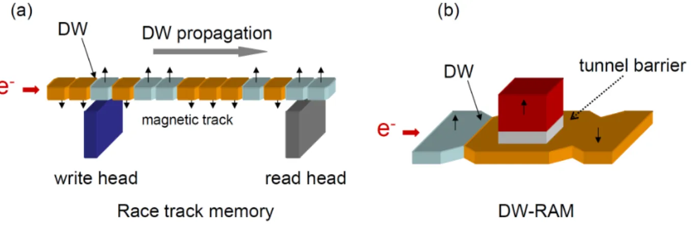
Figure 1.5: Schematics of the device based on current induced DW motion: (a) the race track memory and (b) DW-RAM.
The most famous concept of DW based memory has been proposed by Parkin et al., it is called the race track memory [27]. Basically, this device contains a number of DWs in which each one carries an information bit being shifted synchronously by current pulses along a nanowire (cf., fig. 1.5a). The race track memory has the advantage to combine the high density of the hard disk approach with the reliability of solid state memory. Such device is then operated without mechanically moving parts. A second concept is DW Random Access Memory (DW-RAM) in which the magnetic bit is written through the propagation of a DW in a narrow track while the bit is read using a magnetic tunnel junction (cf., fig. 1.5b) [68]. In principle, this device uses current induced DW motion to switch a bit from P state (“0”) to AP state (“1”). Despite a more complex three terminal architecture compared with standard MRAM, a low writing current is obtained even for relatively high current density due to the small cross-section area of the track. The RAM endurance can be increased since no writing current is flowing in the junction. Using high perpendicularly magnetized materials will be promised to reduce the size of device and increase the thermal stability, altogether with smaller power writing. These two concepts are the DW based counterpart of the MRAM or Spin-RAM based on pillar shaped vertical structures.
1.3
Magnetoresistance effects in nanostructures: Domain
wall detection
The recent trends in nanomagnetism are shifting toward magnetic nanostructures, which are of technological relevance. Nevertheless, detection of the magnetization reversal of such nanostructures is a challenge since the magnetic moment is very tiny (e.g., order of 10−15 -10−141emu for Fe particles of 5-20 nm size [69]). Experimentally, such measurements can not be performed by the conventional magnetometers as vibrating sample magnetometer (VSM) or superconducting quantum interface device (SQUID) since the magnetic signal is well beyond the sensitivity limit of the such magnetometers (sensitivity is order of 10−5 emu for VSM or ~10−7 emu for SQUID) [70]. The MR effects based on the interaction between spin polarized currents and magnetization can provide an easy and fast technique to study magnetization reversal in nanostructures. These techniques are one of most popular way to investigate the magnetization reversal in nanostructures [12, 9, 8, 71, 13].
This part will briefly discuss the use of magnetotransport measurements to detect mag-netization switching and, in particular, to characterize the DW motion in nanostructures. The anisotropic magnetoresistance (AMR) is used to study in-plane magnetized single layer while the use of the extraordinary Hall effect (EHE) is favored for systems with out of plane anisotropy. For multilayer structures, the detection of magnetization reversal can be carried out using the giant magnetoresistance (GMR) effect. GMR measurements can provide infor-mation on the DW position along a nanowire while AMR can only probe the presence of the DW.
1.3.1
Anisotropic magnetoresistance
In a metallic ferromagnet, the variation of resistivity in the presence of external magnetic field typically exhibits the AMR effect in which the resistance depends on the angle between the current lines and magnetization directions. AMR effect which arises from spin-orbit coupling can reach few a percent in some alloys based on 3d metallic Fe, Co, and Ni at room temperature [11]. In general, the resistance is high when the current lines are parallel to the direction of magnetization and low when the magnetization is perpendicular to the current. Let us define
θ the angle between the magnetization and the direction of the current, the resistivity can be
expressed by:
ρ = ρ⊥+ (ρk− ρ⊥)cos2θ (1.12) where ρ⊥and ρk are the resistivities obtained when the magnetization is perpendicular or parallel to the current direction.
1.3. Magnetoresistance effects in nanostructures: Domain wall detection
In in-plane magnetized systems, AMR is thus sensitive to the magnetization components during the reversal process, AMR has been commonly used to investigate magnetization rever-sal in nanostructures, especially in nanowires. The angular dependence of the switching field measurement allows studying magnetization reversal modes in such nanostructures [13, 71, 12]. The presence of a DW within nanowires will induces a change of the total resistance because the magnetization within the DW deviates from the current direction. A local variation of the magnetization direction within the DW with some magnetic moments having a component perpendicular to the current direction results in a lower resistance compare to the saturated state.
Therefore, AMR measurements have been commonly used to detect the presence of DW in nanowires [14, 42]. As an example, Thomas et al.,[43], shows the MR measurement 300 nm wide and 4 µm long NiFe nanowire with a triangular notch patterned on one side of the wire, which acts as a pinning center for the DW (cf., fig. 1.6).
Figure 1.6: Examples of MR curves obtained when the propagation of a DW along a NiFe nanowire is probed by AMR (Figures are reproduced from ref. [43])
In the saturated state, magnetization is parallel to the current flow, the resistance is at the highest level. The partially reversed state corresponds to the injection of a DW into the nanowire that is trapped at the pinning site. This results in a sharp drop of resistance of 0.2 Ω due to the misalignment of the local magnetization within the DW and the current direction. By further increasing the applied field, the DW is driven from the pinning site to the outside of the contacts probes and the resistance reverse back to the saturation value through a sharp increase of resistance (cf., fig. 1.6).
Although the signal is rather small (∼0.04 % [43]), the AMR can be highly sensitive to the details of the DW structure [42, 15]. In particularly, AMR can distinguishes the vortex and transverse wall since they reveal a different component of the magnetization which is perpendicular to the current direction. However, AMR measurements is not sensitive to the
position of DW, it only detects the presence or absence of a DW in between the contacts. Therefore, such measurements can not provide any information about the position and the displacement of the DW. On the other hand, it has been recently showed that the enhancement of shape anisotropy in narrow NiFe nanowires leads to the disappearance of AMR effect [72]. AMR measurement is also quite limited to the study of magnetization reversal in narrow nanowires.
1.3.2
Extraordinary Hall effect
In ferromagnets, the Hall effect consists of two contributions, the ordinary and the EHE [73] being proportional not only to the external field Hext but also to the magnetization M of the ferromagnet. The Hall resistivity ρH is thus described as:
ρH = ρ0H + 4πρSM⊥ (1.13) where ρ0, ρS are ordinary and extraordinary Hall coefficient, respectively. H is the external applied field and M⊥ is the perpendicular magnetization. The ordinary Hall effect is associated to the Lorentz force acting on moving charge carriers. The EHE is related to the spin–orbit scattering in magnetic materials and the effect is much larger than the ordinary Hall effect in metals. Experimentally, when increasing the applied field Hext, ρH changes rapidly at first due to the alignment of the magnetization, and then tends to vary in proportion to the applied field. The constant increment gives the value of ρ0, and the extrapolated value of ρH to
Hext= 0 gives the value of 4πρSM. This analysis shows that EHE measurement can provide the information of the net magnetization in magnetic materials.
For the material with perpendicular magnetization, EHE has been extensively used as a powerful technique to detect magnetization switching in nanostructures [17, 74] and also commonly used to characterize DW motion [18, 45, 32]. Such measurement provide a large signal which allows the precise detection of DW motion within the Hall cross [75]. As an example, Ravelosona et al., [18] shows EHE minor loop in fig. 1.7 corresponding to the reversal of the free layer in spin valve structure by propagation of a single DW through the 200×200 nm2 Hall cross. The variation of the EHE allows detecting the DW motion on a scale as small as 10 nm, such as the jump indicated in fig. 1.7c.
However, it only points out the position of a DW within a Hall cross. Therefore, EHE measurement requires the devices to be patterned into a Hall cross geometry which limits the flexibility of the device structures.
1.3. Magnetoresistance effects in nanostructures: Domain wall detection
Figure 1.7: (c) EHE minor loop corresponding to the reversal of the free layer in a 200×200 nm2 Hall cross. A small EHE jump corresponds to DW motion over 10 nm, the EHE values (1) to (4) refer to the positions indicated in (d) (Figures are reproduced from ref. [18]).
1.3.3
Giant magnetoresistance
GMR was first observed in samples with a large number of repetitions of Fe/Cr bilayers [1], this consequently leaded to the development of spin valve structures in which two ferromagnetic layers are separated by a thin metallic non-magnetic spacer [4]. In such structures, one ferromagnetic layer acts as a free layer in which its magnetization is easily reversed by a small magnetic field. The other one is a reference layer, i.e., its magnetization remains unchanged under a small magnetic field due to a larger coercive field [76].
The mechanism of GMR can be basically understood in terms of spin-dependent resistivity and spin accumulation in magnetic and non-magnetic layers. These origins are closely related to each other and are at the heart of the mechanism of GMR effect which can be presented in the simple picture of the two current models (cf., fig. 1.8).
Figure 1.8: Schematic illustration of electron transport in a multilayer structure for (a) P and (b) AP configuration of two ferromagnetic layers. The solid lines are schematic illustration of individual electron trajectories within the two spin channels. Bottom panels show the resistor network within the two-current series resistor model.
In parallel configuration (P) of the magnetization, one of the two spin channels has a low resistance while the other has a high resistance (cf., fig. 1.8a). Whereas, in anti-parallel configuration (AP), both spin channels have high resistance, since both up spin and down spin electrons are scattered at the interfaces (cf., fig. 1.8b). As a result, the resistance in AP
configuration is larger than that in P configuration. Further details on the GMR effect and
its developments for spintronics application can be found in this review paper [77].
Obviously, the GMR effect reveals that the change in resistance depends on the relative orientation of magnetization of the two ferromagnetic layers. This means that the variation of the resistance is proportional to the amount of reversed magnetization in one of the fer-romagnetic layers. Such measurement provide a powerful technique to detect quantitatively the magnetization reversal in nanostructures. It has been shown that GMR measurement can be used to study magnetization reversal in individual nanostructures as nanopillars [8] or nanowires [9].
During the magnetization reversal of one ferromagnetic layer, the total resistance of the system is given by some average of the resistances in the P and the AP configuration. In the case of spin valve based nanowires, the domains are assumed in series with respect to the current direction then the resistance of this system can be given by [78]:
R = x LR↑↑+
L − x
1.3. Magnetoresistance effects in nanostructures: Domain wall detection
where x is the position of a DW, L is the length of the wire, R↑↑ is the resistance for P configuration and R↓↑ is the resistance for AP configuration. This equation underlines that a simple resistance measurement allows detecting the position of a DW. Experimentally, Ono et
al., [79] has showed an example of GMR measurement to measure DW position in a 500 nm
wide NiFe/Cu/NiFe nanowire (cf., fig. 1.9).
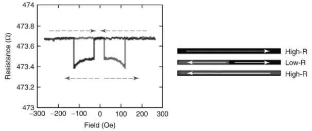
Figure 1.9: Resistance as a function of the external magnetic field of 500 nm wide NiFe/Cu/NiFe wire at room temperature. The magnetic domain structures inferred from the resistance measurement and the direction of the external field are schematically shown (Figures are reproduced from ref.[79]).
Fig. 1.9 shows the variation of GMR as a function of the applied field in which four very sharp leaps are observed. Increase of resistance (state 1) corresponds to the reversal of the free NiFe layer, a plateau of resistance at state 2 corresponds to the pinning of DW on the free NiFe layer. The ratio of the resistance changes from state 1 to state 2 allows measuring DW position where it pinned on the free NiFe layer by using the equation 1.14. Similarly, the DW position on the reference NiFe layer also can be detected based on the ratio of resistance changes from state 3 to 4. This result proved that the GMR is directly sensitive to the position of the DW along the nanowire, emphasizing that such measurement is very attractive for studying DW motion [78]. So far, spin valve structures have been extensively used to characterize the DW propagation in nanowires [79, 9, 18, 29, 33, 67]
However, the presence of the additional layers, i.e., the reference and spacer layers in spin valve structures can give rise to several problems. For example, the shunting of current through the nonmagnetic spacer layer, which is typically much more conducting than the other layers in the stack, results in an inhomogeneous current distribution through the wire. This can also lead to the creation of Oersted fields which might influence the DW dynamics [35].
Arising vertical spin current or mirroring of the DW in the reference layer can alter the DW configurations. These can make the interpretation of the results more complicated.
1.4
Conclusions
In this chapter, we have briefly discussed the configuration of DW structures in magnetic nanowires. The formation of DW structures arise from the interplay between the exchange energy, anisotropy energy and demagnetizing energy which typically showed that transverse walls or vortex walls in nanowires with in plane magnetization and mixing Bloch and Néel configurations in nanowires with perpendicular magnetization.
We then discussed the theoretical models of the DW motion in nanowires driven by the magnetic field which basically showed the different regimes of DW motion. In the case of ideal nanowires without pinning which mostly apply for system with in-plane magnetization, the motion of DW is characterized by two regimes: a steady motion with a high mobility at low field and the precessional regime with a low mobility at high fields. While in the system with narrow DWs, because the pinning is induced by intrinsic defects, the motion of DW is separated by two regimes: a thermally activated regime for fields smaller than the propagation field and viscous regime for applied field higher than the propagation field.
The influence of the current on the DW dynamics was discussed by introducing two spin-torque terms (i.e., adiabatic and non-adiabatic spin spin-torque terms) which are proportional to the gradient of the magnetization in the LLG equation. The adiabatic spin torque term was well understood in term of the conservation of spin angular momentum in which the electron spins exert a torque on the magnetization which leads to the motion of DW. However, the understanding of the microscopic origin and the amplitude of the non-adiabatic torque term is still under discussions. The measurement of the β value shows very much different value depending on the measurement methods and the model used to extract the β term. Also, we shortly presented the concept for new data storage devices based on the current induced DW motion phenomenon.
We finally presented the typical magnetotransport measurements which can provide a good spatial and temporal resolution to detect magnetization switching, in particular, to characterize DW motion in nanowires. This part implied the comparison between the available techniques for the DW detection by AMR, EHE and GMR with the MMR which have been successfully developed in our group. This latter type of measurement will be described in detailed in the following chapters to characterize the motion of a DW for systems with either perpendicular or in plane magnetization.
Chapter 2
Magnetization reversal in FePt based
thin films and nanowires
In this chapter, we will present the investigation on the magnetization reversal of high per-pendicular anisotropy FePt materials with ultrathin DW . We particularly focus on the DW pinning on the structural defects and the dimensionality effect on the magnetization reversal modes of FePt nanostructures [80, 81].
Firstly, we will give a description of the growth and magnetization reversal process in a single FePt thin film and FePt/Pd/FePt spin valve deposited on MgO substrate. Secondly, we will show the effect of nanostructuration on the intrinsic coercivity and the change of the magnetization reversal modes when reducing the dimension of the nanowires. These results emphasis the importance of controlling these reversal modes for next experiment on studying the DW propagation in such nanowires. On the other hand, in view of applications, these effects must be controlled precisely, especially to reach technological nodes below 30 nm when pushing the scalability of DW-based devices towards ultimate sizes.
2.1
FePt based thin films
2.1.1
Growth of a single FePt thin film on MgO substrate
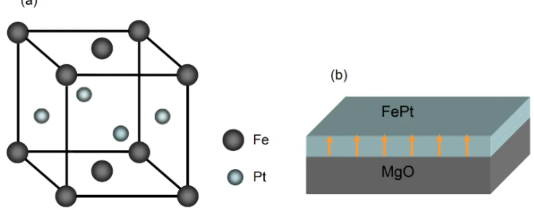
At room temperature, the equilibrium phase of F e50P t50 is in L10 phase (cf., fig. 2.1a). The unit cell is tetragonal and the crystal structure can be described by a stacking of Fe and Pt atomic planes. There is a quadratic axis along the [001] direction corresponding to an easy axis of magnetization. The axial ratio c/a of the lattice parameters is slightly less than one, c/a∼0.96-0.98. In the disordered fcc phase, the Fe and Pt atoms randomly occupy the lattice sites. In the case of FePt L10 phase, we can define an occupancy nF e/F e(or nF e/P t) of Fe atoms in the sub-lattice of Fe (or Pt). The order parameter for the ordered phase is defined
as:
S = hnF e/F e− nF e/P t
i
(2.1) In the ordered phase, the directional short range order is directly responsible for the anisotropy, it can be quantified using the probabilities PF e/F e
In−planeand PF e/F eout−of −plane corre-sponding to the probabilities for a Fe atom having a first neighbor Fe in plane or out-of-plane. In the case of the stoichiometric composition Fe50Pt50, these probabilities vary from P
F e/F e In−plane =Pout−of −planeF e/F e =0.5 for disordered phase to PIn−planeF e/F e = 1 and Pout−of −planeF e/F e = 0 for perfectly
L10 ordered alloy. Experimentally, the long range order can be measured by X-ray diffraction. The short range order which is directly responsible for the magnetocrystalline anisotropy of the L10 alloys is more difficult to measure quantitatively. However, V. Gehanno et al., showed that this directional short range order parameter can be evaluated by using the polarized X-ray absorption fine structure (EXAFS) measurement [82]
Figure 2.1: (a) Schematic of crystallography FePt structure chemically order in the L10 phase, with lattice parameters c = 0.379 nm and a = 0.386 nm. (b) Schematic of FePt films deposited directly on MgO substrate.
The microstructure and magnetic properties of L10 FePd and FePt thin films deposited by Molecular Beam Epitaxy (MBE) on MgO substrates has been extensively studied in our Laboratory: it has been particularly studied in previous PhD thesis [83, 84, 85, 86]. These works showed that the optimized condition to obtain the high order corresponding to the high magnetocrystalline anisotropy of FePt thin film can be of two ways:
+ Growth of FePt film at high temperatures (~500oC) on a Pt buffer layer. In this case, the lattice misfit between FePt and Pt (∼ 1.5%) relaxes through the pileup of a/6 h112i partial dislocations along [111] planes, leading to the formation of microtwins [87, 83].
+ FePt film can be directly grown on MgO substrate(100). In this case, the strain relax-ation process due to the lattice misfit between FePt and MgO(∼ 10 %) occurs by the crerelax-ation
2.1. FePt based thin films
of a dense lattice of dislocations at the interface between the MgO substrate and the FePt layer [88, 86] relaxing in a few atomic layers.
To avoid current passing through the large buffer layer, we choose the second type of FePt layers. We focus here on studying magnetization reversal of 10 nm thick FePt films deposited directly on single crystal MgO (001) substrate (cf., fig. 2.1b). The detail description of experiment process is given in the appendix A. These layers possess a very high perpendicular anisotropy (Ku ∼ 5.106 J/m3), which results on a magnetic configuration composed of perpendicularly magnetized domains separated by a Bloch-type DW. The disorders and defects in these layers arise either from local change in the chemical ordering of the L10 phase or from crystal relaxation due to the misfit between the FePt lattice parameter and that of MgO substrate.
2.1.2
Magnetization reversal of a single FePt thin film
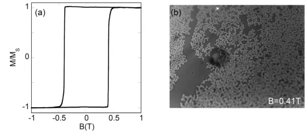
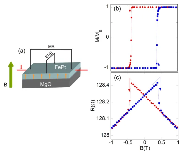
Following the layer growth, the magnetization reversal process of as-deposited samples were studied using macroscopic EHE and polar Kerr microscopy measurements. Hysteresis loop of 10 nm thick FePt was studied by EHE at room temperature using the lock-in technique with an external field applied perpendicularly to the layer. As showed in fig. 2.2a, the hysteresis loop of the FePt layer exhibits a square loop with full magnetic remanence. The coercivity of 10 nm thick FePt films are around 0.4 T. The square hysteresis loop indicates that the magnetization state is unchanged from high fields collinear to the magnetization down to the value of the negative field corresponding to the magnetization reversal. It emphasize that there is no change in the magnetization when the applied field is reduced to zero fields. This allows the observation at any intermediate states of the reversal process at zero field using magnetic microscopes.
The high coercive field and the fullness of the magnetic remanence in such layers imply (cf., fig. 2.2a) that the DWs are tightly pinned on defects. Structural studies showed that the strain relaxation process occurs by the creation of a lattice of dislocations at the interface between the MgO substrate and the FePt layer [85]. These defects could interact with DWs through magnetoelastic coupling. It has been showed by numerical simulations [88] that the anti-phase boundaries can also pin efficiently the DWs in FePt layers.
In the following, the magnetization reversal of the FePt thin films is studied by polar Kerr microscopy (cf., fig. 2.7b). The magnetic domain structure is imaged in a remnant state after applying field pulses. The sample is initially saturated in one direction by a strong field (∼ 1.5 T), we then apply a sequence of field pulses in the opposite direction to create a partially reversed state of magnetization. Fig. [2.2b presents the typical domain configuration occurring during magnetization reversal. The Kerr image shows that the reversed domain (“white” domain) expands by DW propagation. Note that the white domain is connected.
Figure 2.2: (a) Room temperature hysteresis loop measured in perpendicular field using EHE. (b) Polar Kerr microscopy image of a 10 nm thick FePt in partially reversed state showing that the reversed domains grows with dendritic structures. The sample was initially saturated by a negative field, the domain structure is obtained after applying a field pulse of 0.41 T with a pulse duration of 7 µs. The reversed domain appears in “white” domain. The size of Kerr image is 170×130 µm2.
This means that all the white domain could originate from a single nucleation center. Furthermore, there can be large unreversed areas, which imply that the distance between nucleation centers is much larger than 100 µm. As seen previously [89], the structure of the reversed domain leads to fractal configurations.
Based on the model of invasion percolation without trapping (IPWT) [90], Attané et al., [89] demonstrated that this fractal geometry of magnetic domain does not depend on the structure of the lattice (quasi-square lattice of structural defects for FePt/Pt: microtwins or isotropic defects distribution for FePt/MgO: dislocation or antiphase boundaries), it is part of a universality class process.
Basically, this model can be simply described as the schematic in fig. 2.3. The formation of structural defects during epitaxial growth process in FePt sample can be characterized by a distribution of numbers corresponding to the strength of defects, “N” corresponds to the nucleation center for the reversed domain.
At large scale, it is considered that the disorder strength is much larger than the exchange and demagnetizing fields. For a given applied field, only a portion of the sites (those for which
B(t) + hi > 0 where hi is the random static field and Bt is the uniform field that drives the domain growth [89] can be reversed (“white” part). Consequently, in IPWT problem [90], the pressure and the resistance to fluid invasion can be replaced, respectively, by the magnetic field and the local coercivity values hi. Note that the invasion percolation process occurs without trapping. Indeed, and contrarily to the initially proposed case of two incompressible fluids, in a magnetic layer a trapped unreversed domain, i.e., an unreversed domain surrounded by
2.1. FePt based thin films
a reversed domain can be reversed if the magnetic field increases (cf., fig. 2.3b) [89]. The reversed domain growth directions are basically selected as the easiest paths for the motion of the DW, which try to get around the defects possessing the highest pinning strengths (cf., fig. 2.3c,d). Therefore, the generated percolating cluster is similar to those obtained in standard percolation.
Figure 2.3: Schematic of an invasion percolation without trapping (IPWT) model to explain the magnetization reversal mechanism in FePt sample. The set of number corresponds to the strength of local coercitive field, “N” corresponds to the nucleation center. The “white” part is reversed domain and “grey” part is unreversed domain. One can see that the reversed domain propagates in the direction of the easiest paths when increasing applied field. For example: (a) Without reversal at H=0. (b) H=0.3, reverses the parts connected with the nucleus having a local coercivity lower than 0.4. (c) Reversal for H=0.5. (d) Finally H=0.6 reverses half of the layer by avalanche.
Further study using simulation, Attané et al., [89] also elucidated that the fractal structures are qualitatively similar to the experimental results at large scale. At short distance, the effect of the demagnetizing field is found to be crucial, creating the dendritic pattern, i.e., small unreversed domain embedded in the reversed domain that is observed in fig. 2.2b. However, for the large distance, the measurement of the fractal dimension of the reversed domain showed that properties of the percolating cluster are not influenced by the demagnetizing field.