HAL Id: hal-00189282
https://hal.archives-ouvertes.fr/hal-00189282
Submitted on 20 Nov 2007HAL is a multi-disciplinary open access archive for the deposit and dissemination of sci-entific research documents, whether they are pub-lished or not. The documents may come from teaching and research institutions in France or
L’archive ouverte pluridisciplinaire HAL, est destinée au dépôt et à la diffusion de documents scientifiques de niveau recherche, publiés ou non, émanant des établissements d’enseignement et de recherche français ou étrangers, des laboratoires
MEMS TUNABLE CAPACITORS WITH
FRAGMENTED ELECTRODES AND ROTATIONAL
ELECTRO-THERMAL DRIVE
A. Mehdaoui, M. Pisani, D. Tsamados, F. Casset, P. Ancey, A.M. Ionescu
To cite this version:
A. Mehdaoui, M. Pisani, D. Tsamados, F. Casset, P. Ancey, et al.. MEMS TUNABLE CA-PACITORS WITH FRAGMENTED ELECTRODES AND ROTATIONAL ELECTRO-THERMAL DRIVE. DTIP 2006, Apr 2006, Stresa, Lago Maggiore, Italy. 6 p. �hal-00189282�
MEMS TUNABLE CAPACITORS WITH FRAGMENTED ELECTRODES AND
ROTATIONAL ELECTRO-THERMAL DRIVE
A. Mehdaoui
1,2, M.B. Pisani
2, D. Tsamados
2, F. Casset
1,3,P. Ancey
1, and A.M. Ionescu
2 1ST Microelectronics, Crolles, France
2
Electronics Laboratory, Swiss Federal Institute of Technology Lausanne, Switzerland
3CEA/LETI, Grenoble, France
ABSTRACT
This paper reports on the design, simulation and fabrication of tunable MEMS capacitors with fragmented metal (AlSi 4%) electrodes. We examine a rotational electro-thermal actuation. An analytic model of the rotational effect thermal actuator was established in order to show the periodicity of the capacitance when the angle increases. Evaluation of the impact of fringing fields on the capacitance has been carried out using finite element analysis (FEA). The MEMS capacitors were fabricated using metal surface micromachining with polyimide sacrificial layer. The maximum rotation, corresponding to a maximum angle of 7°, was obtained near 1.2 V and 299 mA. The proposed capacitor has a practical tuning range of 30 %. FEA has shown that this figure can be improved with design optimization. The MEMS architecture based on rotational effect and fragmented electrodes does not suffer from the pull-in effect and offers a practical solution for future above-IC capacitors.
Key Words: MEMS tunable capacitor, rotational
electro-thermal actuations, Above-IC integration.
1. INTRODUCTION
Many types of MEMS tunable capacitors have been proposed over the last years, essentially focusing on new architecture solutions to increase their tuning range. Two or three parallel plate capacitors with vertical electrostatic actuation (air-gap variation) show a limited tuning range due to the pull-in effect (non equilibrium between electrostatic and elastic forces) [1-2]. Some other works [3-4] have demonstrated effective solutions by varying the effective area or dielectric constant of capacitors. This paper reports on the design, simulation fabrication of tunable capacitors with fragmented metal
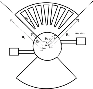
(AlSi 4%) electrodes that are rotationally driven by electro-thermal actuators and avoid the pull–in effect. The proposed new capacitor is shown in Fig. 1. It is made of two fragmented electrodes: (i) a bottom fixedelectrode and (ii) a top rotationally movable electrode suspended over a 1.4 µm air gap. Both metal electrodes have a circular comb form and the top electrode is rotationally driven by electro-thermal actuators. We used two arms connected on each part of the small central diskstructure to rotate the top electrode and change the capacitance. The electro-thermal drive gives more flexibility in terms of design, dimensions and applied voltages. However, this comes at the price of an increased power consumption compared to the classical tunable capacitor configuration.
2. MEMS CAPACITOR WITH FRAGMENTED ELECTRODES AND ROTATIONAL ELECTRO
-THERMAL ACTUATION 2.1. Analytic modeling and simulation
The schematic of a MEMS capacitor with fragmented electrodes using arms electro-thermal actuation is presented in Fig. 2. We used two arms connected on each part of the small central disk structure to rotate the top electrode and change the capacitance. When a current passes through the arms, the injected power induces a net thermal expansion of the arm
T
l
l
=
∆
∆
α
, α is the thermal expansion, l the length of the beam and ∆T the thermal gradient that creates a moment that rotates the entire structure. The amplification (effective displacement of the outer disk) depends on the dimensions of the actuator and the ratio between the radius of the inner and outer disk. We have designed electro-thermal actuators with various dimensions and a case study is presented on the following geometry of arms: width = 4 µm, length = 200 µm and thickness = 4 µm. Fig. 1 shows the shape and the area ofA. Mehdaoui, M.B. Pisani, D. Tsamados, F. Casset, P. Ancey, A.M. Ionescu
MEMS TUNABLE CAPACITORS WITH FRAGMENTED ELECTRODES AND ROTATIONAL
ELECTRO-THERMAL DRIVE
each part (fragmented and non-fragmented). The effective area of the tunable capacitors has a straightforward dependence on the rotation angle, which can be expressed mathematically, as follows : 2 1
.r
S
=
π
,
360
)
).(
.(
.
2
2 0 1 2 2 2 eR
R
S
=
π
−
θ
−
θ
,
360
)
).(
.(
.
2
2 2 0 3 3 er
R
S
=
π
−
θ
−
θ
,360
).
).(
.(
.
2
' 0 2 1 2 2 4N
R
R
S
=
π
−
θ
−
θ
e and the total areais calculated as:
S
=
S
f+
S
nf , withS
f=
S
4 and3 2
1
S
S
S
S
nf=
+
+
, respectively the area of fragmented and non-fragmented surface. The capacitance is)
(
0 nf f nf fS
S
d
C
C
C
=
+
=
ε
+
,C and
fC
nf have respectively a periodic and linear variation when the rotational angle increases . R1 = 190 µm, R2 = 210 µm, R3= 60 µm, r = 10 µm, θ0 = 85°, θ0’= 5°, d = 1.2 µm.
θ0, θ0’ and θe are the initial-state angle of the top
electrode, the initial angle of the finger and the rotational angle respectively. N is the number of fingers.
Figure 1. Rotational effect thermal actuator
The capacitance as a function of θe has been studied by
finite element analysis (ANSYSTM).
Fig. 2 shows the periodicity of the capacitance when the angle increases, with the minimum value periodically decreasing because of the decrease of S2 and S3, which
are the non-fragmented parts of the disk area. We compare the analytical and simulated tuning range results.
Figure 2. Capacitance versus angular displacement For an angular displacement of 7°, we obtained, for the analytical and simulated results, a tuning range more than 70% and 30%, respectively. This discrepancy between analytical and simulated results is due to the fringing capacitance, which is not accounted for in our model. Moreover this tuning range is limited by the design of the capacitor (area) and the buckling in the arm. By a proper design (minimization of S1, S2 and S3 and more favorable fragmentation) this can be increased in excess of 100%.
2.3. Optimization
The design has been optimized by FEA, using ANSYSTM
simulator. The optimization goal was to obtain the maximum tuning range. So, the fringing capacitance should be minimized. First, we studied the influence of, θ0’, then, the angle between two fingers (pitch), and
finally the surface of the non-fragmented areas.
2.3.1.Influence of the angle
θ
0'
The design presented in Fig. 1 was used as a base for the optimization. First we have tried to increase the tuning range by changing the angleθ0’. Each finger is distant by
θ0’. Fig. 3 shows the capacitance versus the angular
displacement for different values of θ0’. Anchors r R3 R1 R2 θ 0 θ0’ 0.1 0.3 0.5 0 5 10 15 Angle (°) C a pacitance (pF) simulation analytic
0.25 0.3 0.35 0.4 0.45 0 5 10 15 Angular displacement (°) C ap acit an ce ( p F ) 5° 7° 10° 13°
Figure 3. Capacitance versus angular displacement for
different angle θ0’
Table 1 shows the tuning range for these 4 angles θ0’. We
can see that the tuning range is optimal for θ0’=13° in
case of a rotation of θe =13°. θ0’ (°) TR (%) 5 29 7 39 10 52 13 64
Table 1 : Tuning range of the Tunable Capacitor for
different angle θ0’
2.3.2. Influence of the pitch
In this part, the influence of the interdigital angle is studied (pitch). Three cases have been investigated : fingers of 5°, 7° and 9° with separating angle of 7°, 9° and 11° respectively. Fig. 4 shows the capacitance versus the angular displacement for different values of pitch.
0.12 0.17 0.22 0.27 0.32 0.37 0.42 0 5 10 15 Angular displacement (°) Capacitance (pF) 5°-7° 7°-9° 9°-11°
Figure 4. Capacitance versus angular displacement for
different value of pitch.
Table 2 shows the tuning range for these three cases. We can see that the tuning range is the most interesting for structures with fingers of 9° spaced by 11°. With this design we can obtain a maximum tuning range of 60%
θ0’ (°) pitch(°) TR (%)
5 7 40
7 9 46
9 11 60
Table 2 : Tuning range of the Tunable Capacitor for
different value of pitch
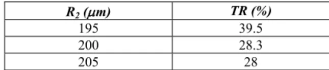
2.3.3. Influence of the non-fragmented area
We keep the optimal angle θ0’ = 13°. The pitch is 13°.
We tried to minimize the area of the non fragmented part, by using a ring of 5 µm width as the middle part instead of a full circle. Then, we simulated the capacitance versus angular displacement for different values of R2.
Table 3 shows the tuning range for three values of R2.
R2 (µm) TR (%)
195 39.5 200 28.3 205 28
Table 3 : Tuning range of the Tunable Capacitor for
different value of R2
To minimize the fringing capacitance and increase the tuning range, one solution is to minimize the non – fragmented area. The drawback in this case is that the
total capacitance is diminishing.
2.3.4. Conclusion of the design optimization
To obtain a maximum tuning range, we have to minimize the fringing capacitance. For that, three possible approaches exist :
- increase the angle θ0’
- increase the angle between two fingers - minimize the non fragmented area
Finally, we find a new optimized design with a tuning range of more than 100% (110%). Fig. 5 shows the capacitance versus angular displacement for fingers of 9° separated by 11° and R2 = 195 (µm) . 0.1 0.15 0.2 0.25 0.3 0 5 10 15 Angular displacement (°) Capacitance (pF)
Figure 5. Capacitance versus angular displacement
A. Mehdaoui, M.B. Pisani, D. Tsamados, F. Casset, P. Ancey, A.M. Ionescu
MEMS TUNABLE CAPACITORS WITH FRAGMENTED ELECTRODES AND ROTATIONAL
ELECTRO-THERMAL DRIVE
3. FABRICATION USING POLYIMIDE SACRIFICIAL LAYER
Fig.6 depicts the simplified successive steps of the process with AlSi 4%. The silicon substrate is p-type with resistivity larger than 8kΩ.cm.
This process needs three levels of masks and one chemical-mechanical polishing step (CMP).
First a silicon dioxide layer (with a thickness of 2 µm) is grown in a wet atmosphere as shown in Fig. 6a. The next step, as shown in Fig. 6b, is the deposition of AlSi 1% bottom electrode (1 µm). The patterning of AlSi 1% metal layer is performed by a chlorine-based plasma chemistry (Fig.6b). Then, a spin-on polyimide layer (pyralin PI –2610 from Dupont) defines the sacrificial layer (Fig. 6c). We use a solution of 3-aminopropyltriethoxysilane on isopropyl alcohol as adhesion promoter before the deposition and a long post-deposition bake of 200°C/1h followed by 300°C/1h in nitrogen atmosphere to have a solvent-free polyimide film [5]. A CMP is needed to level the sacrificial layer (Fig. 6c). Then, a step consists in etching through the polyimide layer (plasma O2) to prepare the mechanical
anchors to the bottom electrode for the suspended electrode (Fig. 6d). The next step of the
etching through the polyimide layer (plasma O2) to
prepare the mechanical anchors to the bottom electrode for the suspended electrode (Fig. 6d). The next step of the process consists in metal layer deposition AlSi 4% (4 µm) by sputtering (Fig. 6e). The patterning of AlSi 4% metal layer is performed by a chlorine-based plasma chemistry (Fig.6e). Then the suspended metal membranes are released by dry etching of the polyimide sacrificial layer in oxygen plasma (O2) as shown in Fig. 6f.
Figure 6. Fabrication process of fragmented AlSi
4% tunable capacitor using polyimide sacrificial layer
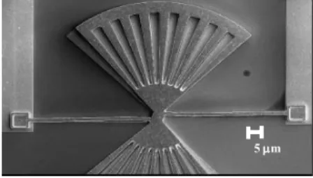
4. CHARACTERIZATION
Figure 7 shows an SEM image of the MEMS tunable capacitor with electrothermal actuator. Figure 8 shows the top fragmented electrode. Figure 9 shows a cross section of 1 µm AlSi 1% + 1.2 µm air gap + 4 µm AlSi 4%.
Figure 7. SEM image of the MEMS tunable
capacitor with electro-thermal actuator
Figure 8. SEM image of the top fragmented electrode
Figure 9. Cross section of 1 µm AlSi 1% + 1.2 µm air gap + 4 µm AlSi 4%
For our fabricated MEMS capacitors (Fig. 7-8-9) the input power need for actuation ranges from 0 to300mW, whichturns into an operating voltage range of 0 to 1.2 V. At zero voltage, the bottom and top electrode are intentionally misaligned. When increasing the applied voltage, the capacitance decreases and increases again (Fig. 10).
Bottom electrode
AlSi1% Top electrode AlSi 4%
Air Gap
Oxide 1 µm
a. Wet Oxidation
b. AlSi 1% SputteringandPatterning (plasma Cl 2 / BCl3)
c. Polyimide Deposition and CMP (Sacrificial Layer)
d. Polyimide Patterning (Plasma O2)
e. AlSi 4% Sputtering and Patterning (plasma Cl 3 / BCl3 )
f. Polyimide release (Plasma O2)
1 µm
0.4 0.44 0.48 0.52 0 0.2 0.4 0.6 0.8 1 Tuning Voltage (V) Capacitance (pF)
Figure 10. Capacitance versus tuning voltage
(experiment)
The measurements have been carried out by extracting the capacitance from S-parameter measurements made in the 2-5GHz range (see also Fig. 11) with a network analyzer HP 8719 D. We obtain a maximum rotation near 1.2 V and 299 mA: the bottom and top electrode being aligned.
Figure 11. Capacitance versus frequency (experiment)
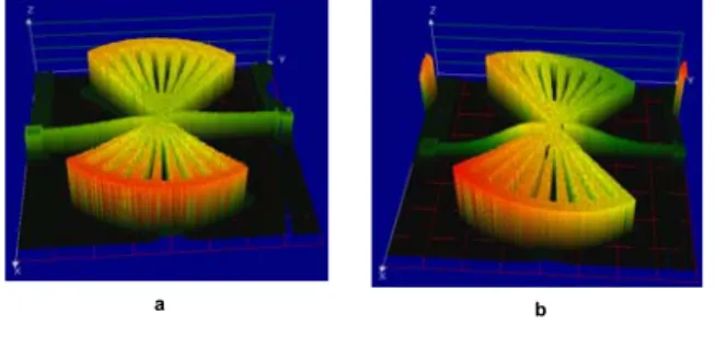
However, this maximum displacement is limited by buckling in the arms at high temperature (>400°C) (Fig. 12).
Figure 12. Microscope picture of the structure :a. under
zero voltage, b. under 0.8V and 270 mA, c. under 1.2 V and 299 mA
By combining electrical measurements with optical profilometry during actuation, the interpretation of figure 10 characteristic becomes clearer. Comparing the behavior of the real structure to the simulated device (Figure 3), we can observe the following:
- The general trend shown by FEA, decrease of the capacitance and then increase, is reproduced in the experiment.
- The value of the measured capacitance is higher than in simulation or that predicted analytically. This could be attributed to the influence of the parasitic capacitances. Further, experiments should clarify this issue.
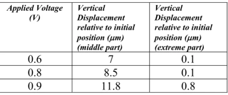
- At 1V of polarization, the profilometer shows that the bottom and top electrodes are aligned. So, we would expect to get the highest capacitance as predicted by FEA and analytical model. However, experimental data show that although electrodes are aligned, the capacitance is lower than for 0V. In addition, profilometer measurements during actuation show that the structure begins to move out of plane even for a 0.6V bias, increasing the gap and therefore decreasing the total capacitance (Fig.14, Table 4).
The reason for this behavior can be found in the mechanics of the structure. The central part of the top electrode is free to move vertically, so the total suspended length of the actuation beams becomes quite considerable. Thermal stress in the beams, which is compressive in our case, increases with voltage, and as a result when this stress goes beyond the critical value for buckling, the whole structure moves up instead of turning. A solution to this problem has been found by changing the position of the actuators and optimization of their design is under way. Figures 14a and 14b show the profile measurement of the top electrode, at 0V and 0.9V respectively.
Figure 13. Profile measurement of the top electrode :
a. under zero voltage, b. under 0.9V. Vertical displacement occurs increasing the gap and decreasing
the total capacitance
a b c c a b 0.4 0.5 0.6 0.7 0.8 2 2.5 3 3.5 4 4.5 5 Frequency (GHz) Ca pa ci ta n ce (p F ) 0 V 1 V 800mv
A. Mehdaoui, M.B. Pisani, D. Tsamados, F. Casset, P. Ancey, A.M. Ionescu
MEMS TUNABLE CAPACITORS WITH FRAGMENTED ELECTRODES AND ROTATIONAL
ELECTRO-THERMAL DRIVE
Applied Voltage (V) Vertical Displacement relative to initial position (µm) (middle part) Vertical Displacement relative to initial position (µm) (extreme part)0.6 7 0.1
0.8 8.5 0.1
0.9 11.8 0.8
Table 4. Vertical displacement relative to initial position 4. CONCLUSION
In this paper, we validate for the first time the principle of the rotational electro-thermal actuator for MEMS tunable capacitors showing 30% experimental tuning range.The experimental maximum angle is obtained at 7°, so less than one period. The experimental tuning range is somewhat smaller than the 70% predicted by simulation and the analytical model developed. We attribute this to the influence of parasitic capacitances.
Optimization of the design has been studied. By implementing certain design changes a tuning range of the capacitance of more than 100% should be obtainable. The MEMS architecture based on rotational actuation and fragmented electrodes does not suffer from pull-in limiting effects, characteristic of conventional tunable capacitors, and offers a practical solution for future above-IC MEMS varicaps.
REFERENCES
[1] D.J. Young and B.E. Boser, ‘A micromachined
variable capacitor for monolithic low-noise VCOS’, Solid-State Sensor and Actuator Workshop, pp 86-89,
1996.
[2] A. Dec and K. Suyama, ‘Micromachined
Electro-Mechanically Tunable Capacitors and their applications to RF IC’s’, IEEE Transactions on
Microwave Theory and Techniques 46 (12), pp. 2587-2596, 1998.
[3] J-B Yoon and T.-C. Nguyen, ‘A high Q Tunable
Micromechanical Capacitor with movable dielectric for RF Applications’, IEDM 00-489, 2000.
[4] Q. Liu and Q.-A. Huang, ‘Micromachined variable
capacitors with laterally positioned suspended plates’,
Proceedings of SPIE, vol. 4601, 2001.
[5] M.B. Pisani and al., ‘Copper/Polyimide fabrication
process for Above-IC integration of high quality factors inductors’, Microelectronic Engineering 73-74,
pp. 474-479.
Acknowledgements
Thanks to the EPFL-CMI staff for the support given on the technological steps development.