HAL Id: hal-01928830
https://hal.archives-ouvertes.fr/hal-01928830
Submitted on 30 Nov 2018
HAL is a multi-disciplinary open access
archive for the deposit and dissemination of
sci-entific research documents, whether they are
pub-lished or not. The documents may come from
teaching and research institutions in France or
abroad, or from public or private research centers.
L’archive ouverte pluridisciplinaire HAL, est
destinée au dépôt et à la diffusion de documents
scientifiques de niveau recherche, publiés ou non,
émanant des établissements d’enseignement et de
recherche français ou étrangers, des laboratoires
publics ou privés.
Evidence of strong carrier localization below 100 K in a
GaInNAs/GaAs single quantum well
L. Grenouillet, C. Bru-Chevallier, G. Guillot, P. Gilet, P. Duvaut, C.
Vannuffel, A. Million, A. Chenevas-Paule
To cite this version:
L. Grenouillet, C. Bru-Chevallier, G. Guillot, P. Gilet, P. Duvaut, et al.. Evidence of strong carrier
localization below 100 K in a GaInNAs/GaAs single quantum well. Applied Physics Letters, American
Institute of Physics, 2000, 76 (16), pp.2241 - 2243. �10.1063/1.126308�. �hal-01928830�
Reuse of AIP Publishing content is subject to the terms at: <a href="https://publishing.aip.org/authors/rights-and-permissions">https://publishing.aip.org/authors/rights-and-permissions</a>. Downloaded to: 134.214.188.191 on 20 November 2018, At: 08:52
Evidence of strong carrier localization below 100 K in a GaInNAs/GaAs single quantum
well
L. Grenouillet, C. Bru-Chevallier, G. Guillot, P. Gilet, P. Duvaut, C. Vannuffel, A. Million, and A. Chenevas-Paule
Citation: Appl. Phys. Lett. 76, 2241 (2000); doi: 10.1063/1.126308 View online: https://doi.org/10.1063/1.126308
View Table of Contents: http://aip.scitation.org/toc/apl/76/16 Published by the American Institute of Physics
Articles you may be interested in
“S-shaped” temperature-dependent emission shift and carrier dynamics in InGaN/GaN multiple quantum wells Applied Physics Letters 73, 1370 (1998); 10.1063/1.122164
On the origin of carrier localization in quantum wells
Applied Physics Letters 78, 1562 (2001); 10.1063/1.1354153
An analysis of temperature dependent photoluminescence line shapes in InGaN Applied Physics Letters 73, 1697 (1998); 10.1063/1.122249
“Blue” temperature-induced shift and band-tail emission in InGaN-based light sources Applied Physics Letters 71, 569 (1997); 10.1063/1.119797
Temperature quenching of photoluminescence intensities in undoped and doped GaN Journal of Applied Physics 86, 3721 (1999); 10.1063/1.371242
Effect of temperature on the optical properties of (InGa)(AsN)/GaAs single quantum wells Applied Physics Letters 77, 2870 (2000); 10.1063/1.1320849
Evidence of strong carrier localization below 100 K in a GaInNAs
Õ
GaAs
single quantum well
L. Grenouillet,a) C. Bru-Chevallier, and G. Guillot
Laboratoire de Physique de la Matie`re, Institut National des Sciences Applique´es (UMR-CNRS-5511), Baˆt. 502, 20 Avenue A. Einstein, 69621 Villeurbanne Cedex, France
P. Gilet, P. Duvaut, C. Vannuffel, A. Million, and A. Chenevas-Paule
LETI/CEA-G-DOPT 17 Avenue des Martyrs, 38054 Grenoble Cedex 9, France
共Received 20 October 1999; accepted for publication 24 February 2000兲
We report an anomalous temperature dependence of the photoluminescence 共PL兲 spectrum of a 7 nm Ga0.72In0.28N0.028As0.972/GaAs single quantum well. The PL peak energy exhibits an inverted
S-shape dependence with temperature. Below 100 K, the PL integrated intensity shows a temperature dependence similar to that of amorphous semiconductors. The observed anomalous behavior is explained by a strong localization of carriers at low temperatures that could be induced by the presence of nitrogen. Thermal annealing does not significantly change the anomalous temperature dependence. © 2000 American Institute of Physics. 关S0003-6951共00兲04116-4兴
The GaInNAs semiconductor alloy is being intensively studied for both its fundamental properties1,2and its potential for long wavelength optoelectronic device applications.3–5 The incorporation of a low content of nitrogen in GaInAs reduces the band-gap energy significantly and allows emis-sion wavelengths as long as 1.3 m to be reached.6 The GaInNAs/GaAs material system is particularly promising for long wavelength vertical-cavity surface-emitting lasers on GaAs substrates. Such structures have already been reported.4,5However, the N incorporation generally induces degradation of the photoluminescence 共PL兲 properties.6 Therefore, the effect of nitrogen on the PL has to be well understood to be able to grow lasers with low threshold cur-rent densities. In this letter, we show that incorporation of a few percent of N in a GaInAs/GaAs single quantum well
共SQW兲 changes the temperature dependence of the PL
spec-trum significantly. The observed anomalous behavior is ex-plained by strong localization of carriers at low temperatures. In this study, two samples were grown by gas source molecular beam epitaxy on semi-insulating 3 in. GaAs共100兲 substrates: a 7 nm Ga0.72In0.28N0.028As0.972/GaAs SQW
structure and a 7 nm Ga0.72In0.28As/GaAs SQW structure as a
reference sample. Both structures consist of a 350 nm thick GaAs buffer layer grown at 580 °C, the 7 nm SQW grown at 450 °C, and a 50 nm GaAs cap layer grown at 450 °C.7The surface morphologies of the structures are smooth and mirror like. The indium and nitrogen contents were estimated sys-tematically by studying thick ternary alloys 共GaInAs and GaAsN兲 in their strained states using high resolution x-ray rocking curve measurements. So the N percentage incorpo-rated into GaInAs was assumed to be the same as that in the thick GaAsN layer. A 700 °C rapid thermal annealing for 10 min was carried out on the quaternary SQW under N2flow. For PL measurements, the excitation was provided by the 514.5 nm line of an Ar⫹laser focused on a 150 m-diam-spot with a power of 200 mW and chopped at a frequency of
17 Hz. The PL signal was detected through a HRS2 Jobin-Yvon monochromator by a liquid-nitrogen-cooled Ge photo-diode associated with a standard lock-in technique. Photore-flectance 共PR兲 spectroscopy is a modulation technique that enables the determination of intrinsic parameters in the band structure of semiconductors. A PR spectrum is the derivative of the absorption of the semiconductor. It exhibits first-derivative-like features at each direct transition in a SQW. The main optical transition in a SQW between the confined electron level and the confined hole level, called E1H1, can
therefore be determined. PR measurements were recorded with conventional PR equipment.8For low temperature mea-surements, the samples were mounted in a variable tempera-ture closed-cycle helium cryostat. Transmission electron mi-croscopy 共TEM兲 measurements were performed with an Akashi EM002B working at 200 kV.
PL and PR spectra of the as-grown GaInNAs/GaAs SQW are shown, respectively, in Figs. 1共a兲 and 1共b兲 at
dif-a兲Electronic mail: lgrenouillet@cea.fr
FIG. 1. PL共a兲 and PR 共b兲 spectra of the as-grown GaInNAs/GaAs SQW recorded at various temperatures. The solid arrows in共b兲 indicate the E1H1
energy fitted using the first-derivative form of the spectrum. The dashed arrows indicate the probable energy of the transition.
APPLIED PHYSICS LETTERS VOLUME 76, NUMBER 16 17 APRIL 2000
2241
ferent temperatures. The emission peak energy increases only from 0.890 eV at 300 K to 0.914 eV at 8 K. The energy shift between 8 and 300 K is therefore very small: 25 meV. The PR spectrum exhibits first-derivative-like features above 85 K and E1H1 is obtained through a nonlinear fit with a
first-derivative functional form of the unperturbed dielectric function. Below that temperature, the spectrum has a step-like line shape as already observed in InAlAs alloys9 and attribution of the E1H1 energy is less accurate共taken in the
middle of the step and indicated by dashed arrows兲. Figure 2 shows the temperature dependence of the PL peak energy of the GaInNAs/GaAs SQW before and after annealing. It exhibits in both cases anomalous behavior, the so-called inverted S shape: from 8 to 100 K, the emission energy decreases, then increases from 100 to 175 K, and finally decreases again with temperature. This S-shape phe-nomenon has already been observed in alloys such as Ga0.5In0.5P 共Ref. 10兲 and Al0.48In0.52As 共Refs. 11–13兲 in
InGaN/GaN multiple quantum wells14 and in AlAs/GaAs disordered superlattices.15 It was attributed to carrier local-ization. Also plotted in the inset of Fig. 2 is the evolution of the full width at half maximum 共FWHM兲 of the PL peak with temperature, before and after annealing. Most of the increase in the FWHM takes place between 70 and 180 K, that is, in the inverted S-shape region. The annealing reduces the FWHM from 37 to 25 meV at 8 K. It also induces a 45–50 meV blueshift of the emission peak, described elsewhere.16Nevertheless, it does not significantly affect the inverted S-shape behavior and the FWHM dependence with temperature, indicating no major change in the PL processes. The E1H1 energy dependence with temperature
mea-sured by PR in the as-grown GaInNAs/GaAs SQW is also shown in Fig. 2. It does not exhibit S-shape behavior, but, rather, typical behavior that can be fitted by the empirical relation proposed by Varshni:17
Eg⫽E0⫺␣⫻T2/共⫹T兲, 共1兲
with E0⫽0.950 eV, ␣⫽5.9⫻10⫺4eV/K, and ⫽300 K
共dotted line in Fig. 2兲. As the temperature decreases from
300 to 8 K, the energy shift between E1H1 共closed triangles兲
and the emission peak 共closed circles兲 therefore increases, showing that the PL emission at low temperatures arises from levels well below E1H1. At 300 K, the PR transition E1H1arises at an energy lower than the maximum of the PL
peak. But this does not mean that the emission threshold lies higher than the absorption one, since the low-energy side of the PL spectrum remains below E1H1.
Since no inverted S-shape phenomenon was observed in the reference GaInAs/GaAs SQW, in which the temperature variation of the PL energy peak is described by Eq.共1兲 with
E0⫽1.234 eV, ␣⫽5.5⫻10⫺4eV/K, and ⫽300 K, this suggests that the S-shape phenomenon is induced by the in-corporation of nitrogen.
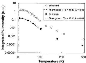
Figure 3 shows the temperature dependence of the GaInNAs/GaAs SQW integrated PL intensity, before and af-ter annealing. Between 8 and 300 K, the integrated PL inten-sity drops by nearly four orders of magnitude. From 8 to 100 K, the quenching of the photoluminescence cannot be de-scribed by an Arrhenius plot, but, rather, by
IPL⫽I0/关1⫹A⫻exp共T/T0兲兴, 共2兲
which is usually valid for amorphous semiconductors in which localization effects occur.18 IPL is the integrated PL
intensity, T the measured temperature, T0 a characteristic
temperature, A a tunneling factor, and I0 the integrated in-tensity at the low temperature limit. Ga0.5In0.5P共Ref. 10兲 and Al0.48In0.52As共Refs. 11 and 12兲 alloys exhibit the same de-pendence at low temperatures, as well as AlAs/GaAs disor-dered superlattices,15 with T0close to 18 and 16 K, the val-ues derived from the as-grown and annealed GaInNAs/GaAs SQW, respectively. This shows further evidence of the local-ization of carriers in the GaInNAs/GaAs SQW at low tem-peratures. Above 100 K, the plot shows a discontinuity, in-dicating that the PL intensity versus temperature exhibits another dependence. Figure 3 also shows that annealing in-creases the PL intensity by one order of magnitude even though it does not change the integrated PL intensity depen-dence with temperature.
FIG. 2. PL temperature dependence of the emission peak of the GaInNAs/ GaAs SQW, before共closed circles兲 and after 共open circles兲 annealing. Solid lines are a guide to the eyes. Closed triangles represent the E1H1energy of
the GaInNAs/GaAs SQW before annealing determined by PR measure-ments; the dotted line is a Varshni fit to these points. The dashed line is a Varshni fit to the closed circles in the 0–100 K region. The evolution of the FWHM of the PL peak with temperature, before共closed circles兲 and after 共open circles兲 annealing is shown in the inset.
FIG. 3. Integrated PL intensity dependence with temperature of the GaInNAs/GaAs SQW emission peak before共closed circles兲 and after 共open circles兲 annealing. Dashed and dotted lines are fits using the relation usually used for amorphous semiconductors.
The phenomena that induce the inverted S-shape behav-ior observed in the GaInNAs/GaAs SQW are now discussed. From 8 to 100 K, the quenching of the PL is typical of strong localization effects and the PL emission comes from energies below E1H1. Furthermore, in the 8–100 K range, the PL
emission peak energy also has a temperature dependence that can be fitted well to Varshni dependence with E0 ⫽0.914 eV, ␣⫽7.0⫻10⫺4eV/K, and ⫽300 K, as shown
in Fig. 2 共dashed line兲. Since coefficients␣andare close to the ones we derived from the E1H1dependence with
tem-perature, we therefore propose that, in this temperature re-gion, the PL emission comes from localized states located a few tens of meV below E1H1 and closely following the E1H1 dependence with temperature. Around 100 K, some
carriers have sufficient thermal energy to reach E1H1, so
radiative recombinations come from both E1H1 and the
lo-calized states. This is consistent with the increase in the FWHM of the broad peak in this region, which may be a sign of two different contributions to the PL peak. This also ex-plains the increase in the PL emission peak energy as the temperature increases and the discontinuity in the plot of PL intensity versus temperature. As the temperature increases again, radiative recombination from E1H1become
predomi-nant: the decrease in the integrated PL intensity follows an-other regime and the PL energy peak decreases again with temperature, with a dependence that approaches the Varshni dependence followed by E1H1.
The physical origin of the localization effect is now in-vestigated. Bright field cross-sectional TEM micrographs of the as-grown ternary and quaternary SQWs are shown in Figs. 4共a兲 and 4共b兲, respectively. Although the reference SQW shows flat interfaces and good homogeneity, it is ob-served from Fig. 4共b兲 that the incorporation of 2.8% nitrogen
induces well width fluctuations from 6 to 12 nm and local strain fluctuations as revealed by the dark field 共400兲 image shown in Fig. 4共c兲. The origin of the localized states, from which originates the PL below 100 K, could be these well width and/or strain fluctuations, since carriers collected by the well preferentially locate in regions where the well width is maximum and/or the local strain minimum. It could also be composition fluctuations 共In- and N-rich cluster regions兲 mentioned by Xin et al.19 or even the existence of highly localized nitrogen-related deep levels in the band gap. How-ever, in all cases nitrogen is most probably responsible for the localization of carriers, because localization effects are not observed in the nitrogen free reference sample.
In summary, both the energy and integrated intensity of the PL peak exhibit anomalous temperature behavior in a Ga0.72In0.28N0.028As0.972/GaAs SQW. This behavior, which
is the consequence of nitrogen-induced localization effects, are not affected by annealing.
The authors thank G. Feuillet, H. Mariette, E. Molva, N. Pelekanos, and Le Si Dang for helpful discussions. This work was supported by a BRITE EuRam program, Contract No. BRPR-CT98-0721, Project No. BE97-4947.
1W. Shan, W. Walukiewicz, J. W. Ager III, E. E. Haller, J. F. Geisz, D. J.
Friedman, J. M. Olson, and S. R. Kurtz, Phys. Rev. Lett. 82, 1221共1999兲.
2P. Perlin, S. G. Subramanya, D. E. Mars, J. Kruger, N. Shapiro, H. Siegle,
and E. R. Weber, Appl. Phys. Lett. 73, 3703共1998兲.
3M. Kondow, K. Uomi, A. Niwa, T. Kitatani, S. Watahiki, and Y. Yazawa,
Jpn. J. Appl. Phys., Part 1 35, 1273共1996兲.
4M. C. Larson, M. Kondow, T. Kitatani, K. Tamura, Y. Yazawa, and M.
Okai, IEEE Photonics Technol. Lett. 9, 1549共1997兲.
5
C. Ellmers, F. Ho¨hnsdorf, J. Koch, C. Agert, S. Leu, D. Karaiskaj, M. Hofmann, W. Stolz, and W. W. Ru¨hle, Appl. Phys. Lett. 74, 2271共1999兲.
6H. P. Xin and C. W. Tu, Appl. Phys. Lett. 72, 2442共1998兲.
7P. Gilet, A. Chenevas-Paule, P. Duvaut, L. Grenouillet, P. Holliger, A.
Million, G. Rolland, and C. Vannuffel, Phys. Status Solidi A 176, 279 共1999兲.
8C. Bru, T. Benyattou, Y. Baltagi, S. Mone´ger, and G. Guillot, J.
Electro-chem. Soc. 93-27, 214共1993兲.
9Y. Baltagi, E. Bearzi, C. Bru-Chevallier, T. Benyattou, G. Guillot, and J.
C. Harmand, Mater. Res. Soc. Symp. Proc. 406, 333共1996兲.
10F. A. J. M. Driessen, G. J. Bauhuis, S. M. Olsthoorn, and L. J. Giling,
Phys. Rev. B 48, 7889共1993兲.
11S. M. Olsthoorn, F. A. J. M. Driessen, A. P. A. M. Eijkelenboom, and L.
J. Giling, J. Appl. Phys. 73, 7798共1993兲.
12
S. F. Yoon, Y. B. Miao, K. Radhakrishnan, and H. L. Duan, J. Appl. Phys.
78, 1812共1995兲.
13I. T. Ferguson, T. S. Cheng, C. M. Sotomayor Torres, and R. Murray, J.
Vac. Sci. Technol. B 12, 1319共1994兲.
14
Y.-H. Cho, G. H. Gainer, A. J. Fisher, J. J. Song, S. Keller, U. K. Mishra, and S. P. DenBaars, Appl. Phys. Lett. 73, 1370共1998兲.
15T. Yamamoto, M. Kasu, S. Noda, and A. Sasaki, J. Appl. Phys. 68, 5318
共1990兲.
16
R. Bhat, C. Caneau, L. Salamanca-Riba, W. Bi, and C. Tu, J. Cryst. Growth 195, 427共1998兲.
17Y. P. Varshni, Physica共Utrecht兲 34, 149 共1967兲.
18R. A. Street, T. M. Searle, and I. G. Augustin, in Amorphous and Liquid
Semiconductors, edited by J. Stuke and W. Brenig共Taylor and Francis,
London, 1974兲, p. 953.
19H. P. Xin, K. L. Kavanagh, Z. Q. Zhu, and C. W. Tu, Appl. Phys. Lett. 74,
2337共1999兲. FIG. 4. Bright field cross-sectional TEM images of the as-grown GaInAs/
GaAs共a兲 and GaInNAs/GaAs 共b兲 SQWs. 共c兲 共400兲 dark field image of the as-grown GaInNAs/GaAs SQW that reveals the strains.
2243