DC-DC Converters with High Efficiency over Wide
Load Ranges
by
Joshua Harlen Bretz
B.S. Electrical Engineering
The University of Michigan, Ann Arbor, 1996
SUBMITTED TO THE DEPARTMENT OF ELECTRICAL ENGINEERING IN PARTIAL FULFILLMENT OF THE REQUIREMENTS FOR THE DEGREE OF
MASTER OF SCIENCE IN ELECTRICAL ENGINEERING AT THE
MASSACHUSETTS INSTITUTE OF TECHNOLOGY FEBlTARY 1999
© 1999 Joshua Harlen Bretz. All rights reserved.
The authorhereby grants to MITpennissionto reproduce
and to distribute publicly, paper and electronic
copies of
t~thesis docu?lent in
~oleown part.
__
Signature of Author: · -
-v·Z '"'"f"' , ./, •••• 'R'' ' ' ' ' r - - - - _ . ,'l\~~k~~~'~f"El~~~i~~'E~~i~~'~ri~~
January30, 1999 MASSACHUSEITS IftJSTITUTE OF TECHNOLOGY Certifiedby: Acceptedby: •• • • • • • • • • • • • • • • • • • • • • • • • • .. • • • • • • • • • • • • • • • •.I~.t • • • • • • • •.1. · · · .. · · · . · · . Anantha P.Chandrakasan Associate Professor of Electrical Engineering Thesis Supervisor
• • • • • .. • • • • • • • • • • • ..~ •.'--~••L; ••• - -;-;-; .. •,r.~• • •/~"""''''--.6-.. _ ••~ . Arthur Clarke Smith Professor of Electrical Engineering Chairman, Committee for Graduate Students
DC-DC Converters with High Efficiency over Wide Load Ranges
by
Josllua Harlen Bretz
Submitted to the Department of Electrical Engineering and Computer Science on January 30, 1999, in partial fulfillment of the requirements for the degree of
Master of Science in Electrical Engineering
Abstract
An integrated switching regulator is presented, including theory of operation, circuit
design, andtestresults. This DC-DCconverter introducesseveralnovel circuits which enable more efficient operation at output powers from l00J.1Wto lW. Efficiency above 80%is achieved from500JlW to 500mW. Specifically, depending on the load current, the regulator automatically switches between Pulse Frequency Modulation (PPM) and Pulse Width Modulation(PWM),and also automatically selects the optimum switching MOSFET. The current sensing is done without an additional current sense resistor. PFM mode operation is synchronous to allow sampled data systems to avoid sampling on switching transitions. In all modes of operation, the regulator output voltage is digitally
programmable. This enablesvariablevoltage achitectures,in which the power supply of a digital system is dynamically changed depending on the throughput requirements, resulting in significantpowerreductions.
Thesis Supervisor: Anantha P. Chandrakasan
Acknowledgments
My graduate study at MIT has been supported by a National Science Foundation
(N·SF) Graduate Research Fellowship, and a research assistantship from the MITEEeS
department. The MIT Ultra Low Power Wireless Sensor Project is fundedbyan ARPA grant.
I \vould like to acknowledge the many people who have helped me over the
course of this project. Thank you all.
• Prof. Anantha Chandrakasan for truly advising well.
• Fellow graduate students Rajeevan Amirtharajah, Jim Goodman, Dan McMahill, Tom
Simon, and Thucidides Xanthoupolos, for helping me with CAD tools, and teaching
me a great deal about circuit design.
• DavidJPerreault, for steering me in the right direction, and teaching me how to do system level behavioral simulations using the MATLAB SlNIULINK toolkit.
• Vadim Gutnik, Scott Meninger, Tom Simon, ~ndThucidides Xanthoupolos, for
working with me during the last weeks before fabrication.
• My family for their'love and support.
Table of Contents
1 Problem Statement and Solution 6
1.1 Improved Battery Life I 6
1.2 Variable Voltage Systems 6
1.3 Widely Variable System Power u 8
1.4 Noise Suppression , I.9
1.5 Solutions 10
2 CircuitTheoryof Operation 11
2.1 BtlCkRegulator Circuit Background u 11
2.1.1 Ripple Current and Voltage 13
2.1.2 Sources of Loss 14
2.1.3 Closed Loop Feedback Control u 16
2.2 Alternative Modes of Operation 18
2.2.1 Pulse Frequency Modulation Mode (PFM) 20
2.2.2 Low Switch Resistance (LSR) Mode I I 26
2.3 Optimal Mode Selection 28
3 Circuit Design 8 • • • • • • • • • • • • • • • • • • • • • • • • •tI • • • • • • • • • • • • • •o ••••~••••••••••••••••••33
3.1 System Reconfiguration 33
3.2 Analog to Digital Conversion e 34
3.3 Pulse Generator "' 37
3.3.1 Fast Clocked Counter Pulse Generator 38
3.3.2 Delay Line Pulse Generator 39
3.3.2.1 Delay Line Element 39
3.3.2.2 Delay Locked Loop Operation 40
3.3.3 Hybrid Pulse Generator 41
3.4 VxComparator 41
3.4.1 Differential Preamplifier 43
3.4.1.1 Programmable Offset 43
3.4.1.2 Common Mode Feedback 44
3.4.1.3 Current Source with Sleep Mode ~ 45
3.4.2 Dynamic Comparator 46
4 Results from Fabricated I C ...•...•...•... 48
4.1 Measured Efficiency Oft • • •48
4.2 PFMoperation 50
4.3 Mode Transitions 52
4.4 Control Power 52
4.5 Layout Plot 52
5 Conclusions and Future
Work ...•...•...
~ 545.1 Future Work 54
5.1.1 PFM-PWM Transition 54
5.1.2 Digital Reference Loading in PFM mode 54
5.1.3 LSR threshold 55
5.1.4 Small switch deactivation in LSR mode 55
5.1.5 LoadTransient Improvement 56
5.2 Conclusions 56
Table of Figures
Figure 1: Variable Voltage Power Supply ~ __ 7
Figure 2: Variable Voltage Feedback Control 7
Figure 3: A Wireless Digital Video Camera ae 8
Figure 4: A representative linear regulator circuit A 11
Figure 5: The Buck switching regulator circuit 12
Figure 6: Output 'voltage ripple in PWM mode 14
Figure 7: Buck converter waveforms 16
Figure 8: Feedback Block Diagram 17
Figure 9: Simulated PWM Efficiency (Semilog) 19
Figure 10: Example PFM waveforms 21
Figure 11: Output voltage ripple in PFM nlode 21
Figure 12: Late NMOS turnoff " 22
Figure 13: Early NMOS turnoff 23
Figure 14: Limit cycles in PFM mode as the output current increases 25
Figure 15: Optimum NMOSgatewidth 27
Figure 16: Power LossesvsNMOS gate width 27
Figure 17: Vx magnified in PWM mode 29
Figure 18: Vx magnified in PWM mode near PFM transition " 30 Figure 19~ System block diagram showing reconfiguration in PFIvI and PWM modes 33
Figure 20: A charge redistribution ADC 35
Figure 21: Charge redistribution configurations 35
Figure 22: A fast clocked pulse generator e . 38
Figure 23: A delay line pulse generator 38
l":4igure 24: A delay line element 39
Figure 25: Delay Locked Loop (DLL) feedback 40
Figure26: Ahybrid pulse generator 41
Figure 27: Differential preamplifier $ e 42
Figure 28: Differential preamplifier and comparator waveforms 43 Figure 29: Dynamic comparator (input from preamplifier) 46 Figure 30: Multi-mode measured efficiency vs. output power (Semilog) 49 Figure 31: PWM-only mode simulated efficiency vs.. output power (Semilog) 49
Figure 32: Yin, Vout, and Vx in PFM mode 50
Figure 33: Transition from PWM to PFM mode 51
Figure 34: Transition to Low Switch Resistance (LSR) mode 51
Figure 35: Layout Plot ~ 53
1 Problem
Statement and Solution
1.1 Improved Battery Life
Switching regulators are often used in battery powered system to create a constant - output voltage even as the battery open circuit voltage diminishes over time. This yields
longer battery life than if the system were powered directly from the battery [1,2]. Since the battery voltage goes down over time, the system would have to be designed to operate at the battery open circuit voltage corresponding to a reasonably large depth of discharge. But, this implies that for the nlajority of time, the systeln is operating at a higher supply voltage than its minimum. This leads to a significant battery life reduction since the power of digital circuitry is roughly proportional to the square of the supply voltage. A switching regulator allows operation much nearer to the minimum system supply voltage for a larger portion of the battery discharge cycle. In this manner, the addition of a switching regulator typically adds at least 20% to the system battery lifetime.
1.2 Variable Voltage
Systems
Indigital systems, the minimum required supply voltage is reduced if the computation can take a longer time [3,4]. Given a workload500/0of the maximum throughput, there are two ways to reduce power. (See Figure 1) First, the computation can be done at speed with the nominal supply voltage, and the system can be powered down for the second half of the given time. Alternatively, the supply voltage could be reduced by about a factor of two, causing the computation time to extend to fill the given time. The second method requires approximately one quarter as much power as the first
method. As the power supply approaches the transistor threshold voltage (Vt),the
increases are not as dramatic since the circuit delay is no longer linearly propnrtional to Vdd •
Fixed Supply
...- - T
frame - -..._
Idle
Efixed= (1/2)CVdd2Variable Supply
... Tframe ., Evar==(l/2)C(Vdd/2)2=(1/4)Et-ixed 1.0 Fixed Supply ~/~le
/ Supply o_~""".,:;;;;;;;,,,--,,,,,."""'-_--,,,,,--...L---'---'--""_~-'---..I o 0.2 0.4 0.6 0.8 Normalized WorkloadFigure 1: Variable Voltage Power Supply
1.004 0.8 eu ~ o Q... 0.6 '"tj 4.) N ~ 0.4
E
o Z 0.2 1.0 Duty Cycle, D[n] - - - . I Desired Rate~
.,
Frequency Digital D[n+l] PWM Power
f--+ I ~ ~ Output
Measure Filter 7 Generator Stage
T
, . - - - . , Matched Vout I L-C I Ring 4- - - -I 1'+---I Filter I Oscillator L---~Figure 2: Variable Voltage Feedback Control
A feedback loop can be made to generate the minimum valid supply voltageby measuring a performance indicator of the system [5]. (See Figure 2) A ring oscillator
can be constnlcted from components identical to the calculated critical path of the digital
sy~tein~ The rest of the system is clocked atthering oscillator frequency. This frequency can be measured and used to control the supply voltage. If the frequency and therefore system throughput is too low, the supply voltage can be raised, and vice-versa. An added advantage is that the system does not need to be designed with an additional built in timing margin to account for process and temperature variations. A constant timing margin can be automatically generated by adding an additional delay to the ring oscillator.
1.3 Widely
Variable System Power
Many battery powered systems have widely changing power requirements over time. A goodexamp~eis a wireless video camera, in which video is captured digitally at a variable resolution, and then compressed and encrypted before transmission over a radio channel. (See Figure 3)
i
Imager &
AID
Video
Compression Encryption Coding
System Power
50()mW-50mW
Figure 3: A Wireless Digital Video Camera
When there is no motion in the field of vision of the camera, the image sel1sor can lower its resolution and there is a very low data rate through the compression, encryption,
and radio channel. Therefore, the standby power can be very low, on the order of
500Jl",l. However, when there is quick motion, successive frames are less correlated, and a large amount of data must be transmitted. Therefore, the active power can be relatively high, on the order of 50mW. Ina s'urveillance application, the times with motion are very valuable. While in standby, the camera must know when to activate and capture these moments. Circuit functionality in both the low and high power regimes is necessary for success.
Often, the system is in standby mode for the vast majority of the time. Ifthis is the case, then the power converter efficiency hl standby mode could determine the overall battery life as much as the efficiency in the active mode.. The power converter must have pigh efficiency over a large range of output power, in this case, all the way from 500JlW to 50mW. Conventional switching regulator architectures do_not achieve this.
1.4 Noise Suppression
Switching regulators can generate a significant amount of conducted and radiated noise. This noise is concentrated at the times when switching events take place. One waytoreduce noise in sampled data systems is to synchronize the system to the
switching frequency of the re~ulator,so that sampling never takes place near a switching event. As will become evident in Chapter 2, synchronization is simple in Pulse Width Modulation (PWM) mode. However, in conventional implementations of Pulse Frequency Modulation(PFM) mode, switching events are not synchronous.
1.5 Solutions
An integrated circuit was fabricated which contains all elements of a switching
regulator except the filter inductor and capacitor. It is designed for output powers from
l00J.lW to lW. Higher efficiency than conventional converters is maintainedatthe power extremesbyautomatically switching to Pulse Frequency Modulation (PFM) mode at low powers, and Low Switch Resistance (LSR) mode at high powers. Switching
events are synchronous even in PFM mode. Inallmodes, the output voltage can be
2 Circuit Theory of Operation
2.1 Buck Regulator Circuit Background
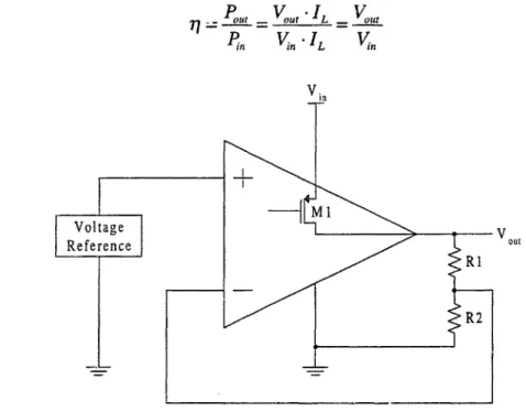
The switched mode power converter is inherently more efficient than a linear
power regulator. A typicallil1ear regulator circuit is shown in Figure 4. The voltage drop
across Ml is maintained as the difference between the input and output voltages. This
voltage drop translates into a large power loss since all the output current goes through
MI. Neglecting the powerQverr1eadof the amplifier,reference, and voltage divider, the
efficiencyis limited to:
~---f+
--l
Ml' - - - 3 1 - - - - + - - -
v
out
L Vout
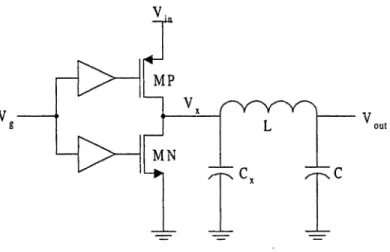
Figure 5: The Buck switching regulator circuit
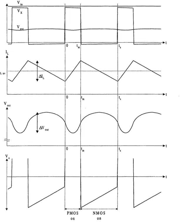
Ina switched mode power supply, there is never a large voltage drop across the switching transistors. The transistor channel widths are made very large, and they are either fully on or fully off. The "buck converter" topology is shown in Figure 5. It is configured to convert a higher voltage to a lower voltage. There are many other possible configurations. For instance,aboost converter creates a highervoltage,and abuck-boost converter creates a negative voltage, which can be larger or smaller in magnitude than the input voltage [6]. The buck converter worksbycreating a pulse-width modulated
(PWM) waveform at the node Vx, as shown in Figure 7. The inductor and capacitor act
together as a second order low-pass filter. They are selected to have a low cutoff frequency with respect to the switching frequency(fsw). Thus, the output of the filter,
VOUhis approximately the DC value of the Vxwaveform. As the duty cycle (D) of this
waveform is increased, the average value of Vxincreases, so Voutincreases.
Alternatively, in the steady state, the current in the inductor must return to the same value after each cycle, and the current increase while the p MOSFET is conducting must equal the current decrease while the n MOSFET is conducting:
2.1.1 Ripple Current and Voltage
In addition to a DC value, Voutalso has a small AC ripple component. This is
since the filter does not completely reject the Vxsignal at the switching frequency. Higher hannonics are filtered out more, so they are not as important as the fundamental frequency. The output voltage ripple istIle integral of the current ripple in the inductor. Both depend on the duty cycle, with the maximum ripple at 50% duty cycle. The inductor current ripple is larger if the switching period is larger, or the inductor is smaller.
~i
=
[V
aut(V. - V
)]!L
=
r
V.
(D - D2)~!L
Lv.
In out L ~ In ~L In A.max V;nts /J.I = -L4L
dVout=
jilL~
dVmax=
Vjnt; out 32LCWhere t5is the inverse of the switc_hing frequency. The inductor current ripple increases
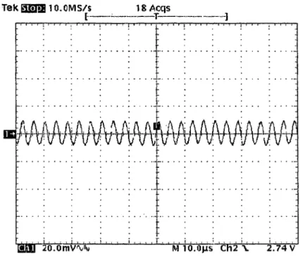
as the switching frequency decreases, or the inductor value decreases. The voltage ripple is inversely proportional to the square of the switching frequency. Figure 6 shows an actual oscilloscope trace of the output voltage ripple.
Tek
am
10..0MS/s 18 Acqs~--.:H·..- ..·----·--T---·-···-..··-· ----....~]
• • I "
Figure 6: Output voltage ripple in PWM mode
2.1.2 Sources of Loss
With ideal components, the switching converter has 100% efficiency.. However,
MOSFETs are not ideal switches. Power is lost in three areas. First, switching the gates
and the Vxcapacitance at the frequency fswcosts:
Where
e
gs is the gate to source capacitance of the n and p channel MOSFETs. exis anumber larger than 1, which represents the total switched capacitance including the
additional capacitance of the gate driver circuits. For instance,ifthe total gate
capacitance of the driver circuits were 30% as large as the gate capacitance of the output
switch itself, then
a
would be equal to 1.30.Pres
= (
I
~av
+
~~
]R
iRd+
R':wD
+
R;w
(1-
D)]
Where L\iLis the inductor current ripple (See section 2.1.1) The duty cycle (D) factors in
since the high and low output switches trade off conducting the output current. Rindis not
related to the duty cycle since the output current always flows through the inductor.
When the average load current is high, the resistive power loss is high. Even when the
average load current is low, there remains a resistive power loss due to the constant
inductor ripple current.
Rswis the channel resistance of the n and p MOSFET switches in the linear region:
Where Jlis the electron or hole mobility,Coxis the gate oxide capacitance per unit area, W and L are the dimensions of the gate,V't is the absolute value of the threshold voltage,
and Vgsis the gate to source voltage a:pplied to the MOSFETwIlen it is on.
Third, there is power lost in the circuits for feedback control and pulse generation.
Put together, the gate switching, resistive, and overhead losses typically place the peak
efficiency of a switching regulator above 90%. However, switching losses dominate at
low output currents, and resistive losses dominate at high output currents. Thus, the peak
o
Voct
o
PMOS NMOS
on on
Figure 7: Buck converter waveforms
2.1.3 Closed Loop Feedback Control
Closed loop feedback control is implemented to synthesize the correct duty cycle
in load current and input voltage. The best controller is constructed using full state feedback, where both the filter inductor current and filter capacitor voltage are monitored. However, measuring the inductor current accurately in continuous time requires a
relatively high gain and bandwidth amplifier, which uses a lot of power. The gainIUllst
be high because the current sense resistor inserted in series with the filter inductor must be small for low power loss. The bandwidth must be relatively high to minimize tracking error of the inductor current. Therefore, for low power converters usually only the
capacitor voltage is used in the feedback loop.
Variable Vref t Vcrr ... Controller Vcont .. PWM D Buck
~ Converter
Reference ~ A~_ " G(s) r D(s)
P(s)
Vout
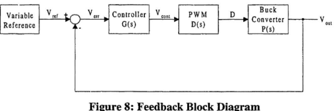
Figure 8: Feedback Block Diagram
A block diagram of the feedback loop is shown in Figure 8. The system transfer functionpeS)from small signal changes in commanded duty cycle to small changes in output voltage exhibits several important features.
v
v.
P(s)= ~t
==
lnL
D
LCs
2+-s+l
RL
Since the average value at Vxdepends linearly onYin,P(s) depends linearly on Yin.
Stability of the closed loop system must be guaranteed for the highestYinpossible since this represents the highest possible gain and therefore the highest unity gain crossover frequency. The transfer function also has a peak at the resonant frequency of the filter. Inthe closed loop system, this peak can cause oscillations if the loop gain is greater than
one that the resonant frequency, assuming integral control. The height of the peak
depends on the damping providedbythe load resistance and the switch resistance. As the output current goes down, the equivalent output resistance goes up, and less damping is provided. Higher switch resistance also reduces the height of the resonant peak. Stability of the closed loop system must be guaranteed for the highest resonant peak possible.
The transfer function D(s) models delays in the control system. There is always a delay in the pulse generation circuit, which can be modeled as one half of a switching period. There is also a delay if the output is sampled discretely, equal to the sampling frequency.
fj
-stdID(s)=
-=--
==
e t a . "Veont
One possible control law is a simple gain and integrator:
V
K
G(s)
=
!-ont =_Verr S
It is possible to use more aggressive control to increase the loop bandwidth, but it comes at the cost of much higher control power overhead [7]. Ina low power converter, the unity gain crossover frequency is typically placed low enough so that there is adequate phase margin, and so that the highest possible resonant peak: does not also have above unity gain.
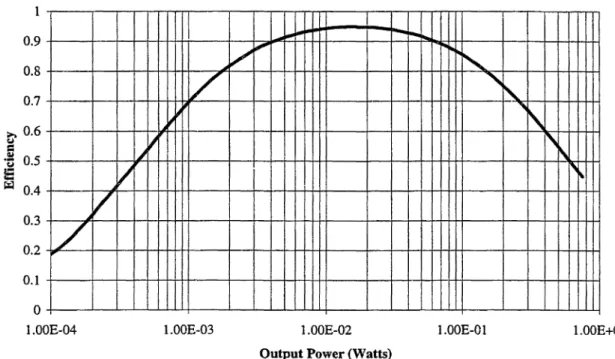
2.2 Alternative Modes of Operation
Different loss mechanisms become dominant in PWM mode as the load current changes. As load current increases, the power lost due to channel resistance goes up. Therefore, at high output currents this loss dominates, and at low output currents it is
negligible. Incontrast, the gate switching losses and control losses are constant with load current. Therefore, these losses dominate at low output currents, and are negligible at high output currents. (See Figure 9)
0.9 0.8 0.7 ~ 0.6 ~
=
.~ 0.5 c....
~ 0.4 0.3 0.2 ..-II ......
-
-...~V
"
...~~...~
V
'--
~ ~~"[\
"
~I
'\
I
,~~r
/
0.1o
1.00E-04 1.OOE-03 1.00E-02
Output Power (Watts)
I.OOE-Ol l.OOE+OO
Figure 9: Simulated PWM Efficiency (Semilog)
To appreciably increase efficiency at the load current extremes, it is necessary to address the corresponding dominant loss mechanisms in architecture decisions. At low load,itis possible to vary the switching frequency. This makes the gate switching losses scale linearly with load current instead of being constant. This technique is called Pulse Frequency Modulation (PFM), and will be explained in the next section. At medium load, traditional Pulse Width Modulation (PWM) mode can be used. At high load it is possible to add larger switches in parallel with the smaller ones to reduce channel losses. This technique will be called Low Switch Resistance mode (LSR), andituses fixed
frequency PWM control. Sectiorl 3.3 will show how it is possible to automatically select the optimal mode for the current output load.
2.2.1 Pulse Frequency Modulation Mode (PFM)
If both output switches were to be turned off when the load current is light, it would take a long time to discharge the output capacitor voltagebytens of millivolts, the size of the current ripple in PWM mode. For instance, at 100J.1A and 1V output, a
19F
capacitor dischargingby lOrnV takes lOOJ.ls.C
dt =dV - = IOOj1S
I
This is much longer than a switching period in PWM mode, which is typically 1~s to Sus. Therefore, it is possible to operate in a mode called Pulse Frequency Modulation (PFM). When it is detected that the voltage is below a given threshold, a single pulse raises the output voltage again. (See Figure 10 and Figure 11)
Vout
o
on NMOS on ---+ NMOS and PMOSoff
o
Figure 10: Example PFM waveforms
Tek
amm
10. OMS/s 8 AcqsE·-·--·---_·_··_·-T···....·_-··..__··_··_-·....__.J · .. :'" : ' . : . . . . ! . ..t. .. .I • • ~ • • • I " I • •
·
.
.
.
.
i·
.
.
- ···r:..· , . t . f:-
'-f:' . . . ...
. .
: < ;\ ).
~
f. ...
~
...
~... ~.
.
~
... -.
.. I--+-!--',
~
:1..++-J++~\}+.++
-+-r-~
\j".I....:'H--f'~
!.+-!-~"I""'I"'I"~'
-++..~
++.-:
:\ J:
:
:
~
.
:
:
~
\
:
-
~: .\j . :
:. ..
~:
:
'... :.. .'
·
.
.
.
.
t
.
.
.
.
..._~ . . . . . r . . ....:....:....:....:....f. ...:....:... -:....
l
To . . . . .Figure 11: Output voltage ripple in PFM mode
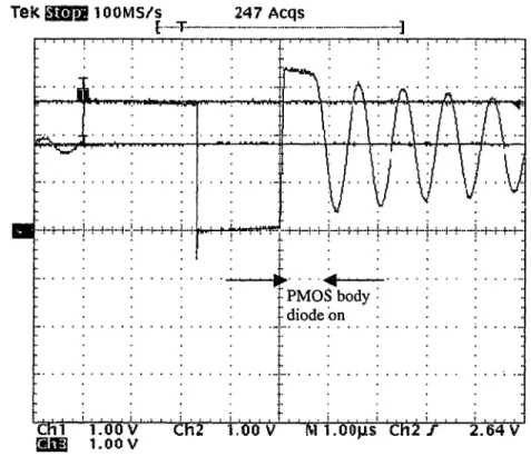
Inorder to maintain peak efficiency, the inductor current (IL)must be near zero at the end of a PFM pulse when both switches are turned off(tsin Figure 10). Ifit is not,
then the inducto]~will either charge or discharge the small node Vxcapacitance (Cx), until
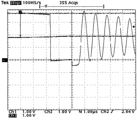
one of the switcli body diodes conducts. The body diode will stop conducting when the inductor current ramps down to zero. If t5is too late, then ILwill have gone negative, charging up Cx tlntil the high side switch body diode turns on (See Figure 12). Ift5is too
early, then
IL
will still be positive, dischargingex
until the low side switchbodydiode turns on (See Figure 13). Either way, the entire power stored in the inductor at the timet5will be dissipate:d in a body diode. However, this stored power decreases as the square of the inductor current. ILis decreasing linearlyillthe region of ts,soift5is slightly
misplaced, then the power stored in the inductor will be small. But, iftsis badly
misplac~d,thell power loss could be high.
Tek
mmJ
100MS/sE·...M·T--·__N__.•__..__._...247 Acqs.._.N._-...._.__._.._--_..._]' : • It : . . . .
f
. . . I . . . .-1 ... , . .' .. ! . . . . : . . . . : . . . . ! . . . . t· ... ! .. . it
• . . 1... ··t·· ..
• • • ... It .. .. ~-!'.+-i-+-!'-!--!-i-"!-;'M+-+.-t..+!-! . : . ; ..'....
-l·-!...
+...!-+-i-+··+..!---~_·~·...~-!·-1...1-·r+·_!·..+M-1--t-.+.+-+... +.~
~_
. ~PMOSbody ~ • • • • J.. • • • . . . i diodeon . . . .... .. . ... . . . .. .. ... . .. . ._~_ . 1: 1 . . . ~ . . . , _ I' 1_ • • • • '" 01 • • " .. tt:
. . . i . . . . i . . . . i . . . . ! . t .... i . .. i .. . f • • • t • e l l .00 V j 2.64 VtiiIl
Tek!mill OOMS/s 355 Acqs E· ···=F-·..·_-_·_-_.._..··..· ·_..·· _··· _···..····,,~·..· ]
t-. t-. t-. t-. t-. : • • • • : + • • • : + • •···f.. .. .
.
1: ~. ...
. ..
... . . ... . ...
~~.... . . . . t· : . . • • • • : ~ + • • : • • • • : • • • • : • • • • •-roo . . . . : . . . . : . . . . : . . . 1:i 1.i ...~ '-1":" .t
. t ,.. . . . + • • • • • • • • • • • • • • '-1:" .t
.. .. II .. it.. • .. • . . . ! -: J ! .: ! :- : ,... C 1 1.00V C 2 1.0 V !\11.00]JS C 2 f 2.64V ~ 1.00VFigure 13: Early NMOS turnoff
The correct tsis a function of Vin, Voutandtm(The time during a pulse when the
low side switch takes over for the high side switch):
Alternatively, given a fixedts,the correct tmcan be derived. Inthe implementation of this timing, it is easiest to maketsexactly equal a PWM switching period. Then, duty cycle can be inherited from the steady state duty cycle in PWM mode. Ifitis possible for Vinto change while in PFM mode, then the proper dutycyclecan be calculated given a
meaSllrement ofVine Adivision is required, but since relatively low accuracy is necessary, it can be implemented with a small lookup table.
One disadvantage with the traditional implementation of PFM is that the
capacitor analog circuits are phase locked to the switching frequency so that sampling
does not take place at the same time as a switching event, at which time there is elevated
levels of radiated and conducted noise. IfPFM is implemented so that a simple
comparator initiates each switching pulse, then the overall frequency cannot be predicted,
and thus noise cannotalways be cancelled. However, it is possible to operate in
synchronous PPM mode, where each pulse can startonly at a discrete time. As in fixed
frequency control, the PFM pulse can be locked to a reference clock. This clock can
often be shared with the circuit under power and so therefore represents a negligible
power overhead if the circuit under power is in the same package.
In synchronous PPM mode, the correspondence between pulse duration and
output voltage ripple is different than P"NM mode. If the pulse width is the same in PFM
mode as in PWM mode, then the output voltage change over one pulse will actually be
larger in PFM mode. The total inductor current ripple is unchanged:
di
==[V
our(V. -
V
)~~
=~
7.
(D _
D2)~t.f
L V. In out L LVin
'.JL
InBut, at zero output current, the inductor ripple current goes both positive and
negative in PWM mode. InPPM mode,it is strictly positive, which means that the peak value is twice as high. Therefore, at zero output current, the output voltage ripple will be
four times as large. As the output current increases, the output voltage ripple across one
However, at the same time, a dithering effect occurs since the output voltage is measured
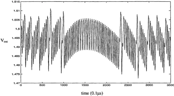
at discrete times. Anexample of this behavior is sho\vn in Figure 14. This dithering effect effectively negates the reduction in ripple due to outptlt current.
1.515 1.51~ -1.505f- -1.5
-Vaut 1.495 1.49 1.485 1.48 1.475 -1.47 0 500 1000 1500 2000 2500 3000 3500 time (O.lJls)Figure 14: Limit cycles in PFM mode as the output current increases
If the ripple in PPM mode is desired to be smaller, it is possible to make each
pulseshorter. This would imply that the timetmwould have tobe scaledbythe same
amount. Since the pulse generator is implemented digitally,it is trivial to do such
operations. Ifeach pulse is shorter, then pulses will be spaced closer together, resulting in slightly lower efficiency. However, the ultimate efficiency at low output currents is
limitedbytheADCand clock circuitry overhead, and therefore will not change. If the output voltage is measured at discrete times,it must be sampled
immediately before the beginning of a candidate pulse. Ifthe measurement is made earlier in the preceding cycle, then the output voltage ripple will be larger. And, if this
delay is larger than a pulse duration, then will be limit cycles in the output voltage. However, the delaydoesnot need to be zero, because the output voltage changes slowly near the end of a pulse. This is since the inductor current is near zero at this time. (See Figure 10) A reasonable delay allows ample time to make a measurement and decide whether to generate a pulse on the subsequent cycle.
2.2.2 Low Switch Resistance (LSR) Mode
For a given output load, there is an optimal switch size which minimizes the combined losses from gate switching and channel conduction. As the switches are made wider, the gate capacitance goes up, and the channel resistance goes down. The
minimum power loss is achieved when the width is selected as follows:
Wpopt =
Where a is a constant accounting for the additional switched capacitance of the gate drivers (See section 2.1.2), and MLis the peak to peak inductor current ripple (See section 2.1.1). Vgs is the gate to source voltage that a transistor has while it is on. It is a
fairly broad minimum, as can be seen in Figure 16, and so it is reasonable to have two discrete switch sizes to choose from. ><Figure>< shows the optimum NMOS gate width given typical parameters.
",-.., ~ QJ 0.1 ... G.' ~"-' .::... 'C ~ CI.) 0.01 0
~
E=
.5
0.001 ...=.. 0 ...-~~~ ~ ~ . / ' -.'
~~,,'" -~ J!I" 'tJ~ ~tI1''''~ ~ 0.0001l.OOE-04 I.OOE-03 1.00E-02
Load Power (Watts)
1.00E-Ot 1.00E+OO
Figure 15: Optimum NMOS gate width
...
~
conduction losse:; switching losses total losses ... .... ... ;...":.":... ...~ ... ".,. . ...':.'''> .::':' ... ... ::; ...0::': ... " : ...: .,., : , / : ,.. . . :- :,;..-'" --:'..:.. 'j" - ) ..; /. · . . · . Switch Optimization ...- ..- .--~..."." ...,., ~.... 4 4.5 3.5 fj) ~ .!. 3 c: a Eo §2.5 .. , ~... - ...y ".... . . ~ : . en ...: • . c:: /' . . . o ... . . U . . Q 2 " : ; _~7 :• • • • • •, • • : • • • • • • • • • • • • • : • • ~ / . ~ . r / / : 1.5 ' ) ..r :... . .. : : . .. 0.5 '".-, ... 1 .. ..,' ;..":'., . ..· .. . · . OL-.-L....---'---L---'- ---'- - - I -_ _~ _ _ ' _ ....J 2 4 6 8 10 Channel Width(meters) 12 14 16 X10-42.3 Optimal Mode Selection
The optimum of three different modes is automatically selected in real time: PPM mode, PWM mode, and PWM mode with wider switches (LSR). This can be done reliably with a low power overhead, without using an external current sense resistor. Implelnentation details ofeacllmode transition will be described, along with suggestions for further improvements.
Conventionally, an external current sense resistor and amplifier are used to meaSlue current. In a novel approach, the channel resistance of the NMOS switch itself can be used to measure the output current. When the inductor current is positive (flowing into the filter capacitor), the node Vxwill be negative while the NMOS ~witchis
conducting. See Figure 7 for switching waveforms. The output current is the average of the inductor current, and the inductor current has a fixed sawtooth ripple amplitude. Therefore, when the output current goes below one half of the inductor ripple current amplitude, the inductor current goes negative near the time ts• Intum, Vxwould be
positive immediately before ts. Immediately after ts,the PMOS switch begins
conducting, and Vxswings near the input voltage. There is a direct relationship between
the voltage at Vximmediately beforets,and the average output current. Given the inductor rijJple amplitude (ML):
Iii
=
[YOU!
(V -
V)~.!L
=
~
T.(D - D
2)~!L
LV.
In outL
LVin ~L
in'. \
V
x1,=1
lii
L'Z )
=
s+
-\ 0 P}':T\1thresh Rn 2 swwhere Rswis theresi~tanceof the NMOS switch. Figure 17 shows an
TekRun: 1001\1515 Sample
[~'.--"-"---_..-"F---"'--'--J
! ..
Figure 17: Vx magnified in PWM mode
v
xcan be sampled immediately beforet5 , from which <io>
can be deduced. A programmable offset can be introduced to the measurement circuit to put <io>
inside a range of currents, which then is used to set the proper operating mode. This circuitremains low power because it can be shut down between measurements. The levels at Vx
are relatively small, which makes the circuit design non-tHvial. However, since the
measurement of Vxalways takes place immediately before a switching event, there is no
switching noise interference in the measurement. With no external current sense resistor,
the differential sense wires can remain on the die, where the are less susceptible to noise.
And, the resistance of the NMOS switch is high compared to that of a sense resistor,
making the signal level at Vxhigher, which also reduces noise sensitivity. Ifthe current
sense resistance were as large as the NMOS switch, then comparable power would be
When the converter is operating in PFM mode, the transition to PWM control must be made whentheoutput current goes above the threshold:
This is because above this threshold, the inductorcurrentnever goes to zero, so there is no opportunitytoturn off both switches. Figure 18 shows the switching voltage
v
x in PWM mode when the output voltage is just above the PFM threshold.Tek Run: 1001\1515 Sample
E-'-"~'.-..----~_.-...-T_-...--.----.--~
. . . . ' ! ! . ! .. ' ! .
... • II .. 0I!.... .. • • II ..
50.0mY l\al 1. 00JJS C 2 '- 600mV
Figure 18: Vx
magnifiedin
PWM mode near PFM transition
IfPFM mode control is maintained at high current, there may be instability as the output voltage oscillates above and belowthe voltage reference. There aretwowaysto
detect the PWM current threshold. First, the node Vxcan be measured at the end of a pulse to see whetheritis above a certain value. The pulse should be the first following a period when both switches are off, to insure that the inductor current starts the pulse period at zero current. This method does not appreciably lower efficiency at low output
currents because no measurementsaremade when there are no pulses. Secondly, the numberofconsecutivepulses can bemonitored. Iftherearetoo manypulsesin arow,
then the output current is approaching the threshold. The second method is susceptible to output voltage oscillation than the first method. Also, as the number of pulses in a row gets larger, oscillatiolt can take place at lower frequencies, and thus becomes more likely. The first method guarantees that the output current is below the threshold, thus
preventing oscillation.
When the converter is operating in PWM mode, the transition to PFM control must be made when the output current is belowIpFMthresh. Vxis monitored at a set interval
to detect the output current. Current does not have to be measured every cycle, to save a small amount of power. To add hysteresis to the transition, the current set point is slightly lower than in the reverse direction. This prevents limit cycles when the output
c~rrentis very near the set point. IfPFM mode control is set up to inherit the dutycycle
of
the PWM mode, then the PWM controller must be near steady state before the transition is made. To insure this, there is a delay on startup and on returning to PWM mode before PFM mode can be activated. The duty cycle can leave steady state when a load transient occurs. But, this is not an issue since PFM mode would only be activated after a step from steady state high current to low current, at which time thedutycycle would not change much since the control bandwidth is low compared to the measurement frequency. And, any small error in duty cycle does not appreciably reduce the efficiency in PFM mode. (See section 3.3)If theoutput current goes above a higher threshold (ILSRthresh+),then wider
switches are activated (Low Switch Resistance Mode or LSR). This threshold should be at the
point
where the big switches are equally as efficient as the small switches:psml
+
psml=
pbig+
pbig sw res ,fW res ,"-'. (csm1- n+
CSml-p)v.2j A·2 1+ :: 1"8 gs gs In sw_.:=!-L
LSRthresh W Rsml- nD+
RJm1-p(1-D) 12 sml sw swWhere Cgsisthe gate to source capacitance of the small n and p channel MOSFETs, Rsw is the
cOITesponding
channel resistance, andL\iLis the inductor current lipple. (See Sections 2.1.1 and 2.1.2) Measurements of PFM and LSR thresholds can be interleaved sothat two comparator circuits are not needed.Once in LSR mode, the resistance of the NMOS power FET changes according to its width, and therefore the reverse thresholdILSRthresh.must be scaled to compensate. In
addition, some hysteresis should be added to prevent oscillation in and out of LSR mode near the threshold..
3 Circuit Design
3.1 System
Reconfiguration
The control logic is reconfigured in two different ways for PWM and PFM
modes. Figure 19 shows how each element is used in the two regimes. The control logic
is implemented digitally. This makes it possible to program loop parameters in real time.
Inboth modes, the output voltage can be changedbythe device being powered, which saves significant power. InPWM mode, the loop gain can also be changed, which is useful since the gain margin changes linearly with duty cycle [8].
PWM mode:
PFM mode:
V.ID
Valli
VDII
In PFM mode, the complexity of the cOl1trolloop is minimized to reduce the power overhead. The duty cycle is fixed at the last value while in PWM mode. For this method to be work, the input voltage must remain relatively constant while in PPM mode. This assumption is valid for battery powered systems, since the battery voltage is unlikely to change quickly, especially
under
low load conditions in PPM mode. The pulse generator and gate drivers areonly
enabled during a pulse. The Analog to Digital Converter (ADC) is reconfiguredtooperate as a variable threshold comparator.In
this configuration, the ADC is faster and consumes less power.3.2 Analog to Digital Conversion
AnAnalog to Digital Converter (ADC) is needed to
measure
the output voltage so thatitcan be compared to the desired value. Seven bit precision is reasonable to make the error smaller than 1%of the input voltage. (The Pulse Generator has eightbitprecision, to prevent limit cycles.) Very low power operation is required at a sampling rate of about 100kHz. The charge redistribution ADC is well suited to this application
64C
I
32cI
16CT
IC
I
4cI
2CT
56 55 $4,.,.. 53 S2 51+
11
11
11
11
1 1
Figure 20: A charge redistribution ADC
EVil
CompOUl
v.
10GND
v.
InSample Mode
Convert Mode
Figure 21: Charge redistribution configurations
Figure 20 shows a representative circuit diagram of the ADC. First, the input voltage is sampled. The node Vmidis connected to Vref, and the bottom plates of all capacitors are connected to Yin. Then, the conversion begins. The node Vmidis left
floating while tile bottom plates of'some capacitors are grounded, and others are connected to Veef. Figure 21 shows this process in a simplified form. A finite state
machine monitors the output of the comparator, and does a binary search by connecting different sets of capacitors Caand Cbto find the closest approximation to the input voltage. Byconservation of charge, the value of Vmidcan be derived:
Qsa~pte=Qco~ver,
=
~c.v. vmld vm,d k ' ,i
(C
a
+CbXV'I!!
-~J=(Ca
+Cb)vmid -CbV'I!!
e
a+2C
bVmid
=
Vrt/ - ~ne
a+C
bThe comparator output will change state when Vmidis equal to Vrefe This is the final
configuration of the converter after the binary search has completed. The ratio of Vinto
Vrefis linearly related to the portion of the total capacitance in the bank that was switched
In this manner, a linear conversion is performed, even though the value of Vmidis not linearwith V
in-The total conversion takes eight cycles. in-The first cycle is when the input voltage is sampled. The subsequent seven cycles comprise the binary search, which establishes a seven bit result. InPulse Frequency Modulation (PFM) mode, the requirements are
slightlydifferent. The result needed is only onebit,which signifies whether the output voltage is higher or lower than the reference voltage. Also, the result is needed very quickly sinceitdetennines the subsequent pulse. It is possible to reconfigure the ADC to meet both these conditions. The samplingtakesplace in the samemanner,but only one comparison is done. The switchesSO-S6are simply connected to reflect the digital voltage reference. IfVinis greater than this reference, then at the input to the comparator,
Inthe full conversion mode, there can be a loss of accuracy for small input
voltage~. The problem is that Vmidcan exceed Vrefduring the conversion. If the voltage
difference is greater than about 0.6 volts, then the body diode of the MOSFET connected
from Vmidto Vrefcan begin conducting. This will change the charge distribution on all the capacitors, and will therefore make the conversion nonlinear. One solution would be bias the substrate of this MOSFET at a higher voltage. Alternatively, the voltage
reference could be lowered. Or, the binary search algorithm could be altered so that Vmid
never getstoohigh. This would make the conversion slightly longer, but would relax restrictions on the reference voltage. Two extra conversion cycles would occur before the other seven, comparingYinto Vref/8 and then V
rer
/4 instead ofVref/2 immediately.Yet another solution would be to connect twopchannel MOSFETs in series, with the body of the MOSFET next to Vmidconnected to its own source terminal. This would put
two body diodes in series, raising the tolerable voltage difference between Vmidto Vrefto
about 1.2 volts.
3.3 Pulse Generator
A pulse generator circuit is need to precisely place a signal edge within the switching period, given a digital duty cycle command value. This edge is used to create the gate waveforms of the output power MOSFETs. The pulse generator circuit
subdivides the switching period into 2M sections, where M is the number of bits in the duty cycle command value. The nature of this process is power intensive, and therefore the circuit requires optimization for power. First, two common approaches will be presented: a fast clocked counter, and a delay line. Then, a power saving alternative will be discussed: a hybrid of these two approaches.
fsw
Load S
PWM
Out
Q
Duty Cycle R Out
(M bits)
Count
Figure 22: A fast clocked pulse generator
3.3.1 Fast Clocked Counter Pulse Generator
Inthe fast clocked counter approach, the desired duty cycle is loaded in to a down-counter clocked at a frequencyfsw2Mwherefswis the switching frequency. (See
Figure 22) When the counter reaches zero, the edge is created. The power of this circuit is at least proportional to2M• The amount of capacitance switched in one cycle increases as 2M• Furthermore, as the clocking frequency increases, the powersupplyof the counter must be increased to satisfy timing requirements. Therefore, if the circuit operates at the power converter input voltage, then there is a limit to the accuracy.
fsw - --I
s
R
Q PWM
Output
3.3.2 Delay
Line Pulse Generator
In
the delay line approach, a delay line is constructed with 2Nelements. (See Figure 23)The
totaldelay
is madeexactly
equal to a switching period. The desired duty cycle selects one of the delay element outputs, creating the timing edge. The power of this circuit is at least proportional to 2N• This is because there are 2Nelements which switch during one switching period. Furthermore, as the delay through a single element decreases, the minimum supply voltage increases. However, this minimum supplyvoltage is lower than with the fast clocked counter approach, since the critical timing path in the counter is much longer. The disadvantage of the delay line approach is that the multiplexer takes up a large area.
Reset
e>1
Out
Figure 24: A delay line element
3.3.2.1 Delay Line Element
Anindividual delay element is made from a current starved inverter, followedby a simple inverter. (See Figure 24) After each use, the Reset input is pulled low, which recharges the inverter input capacitanceC1oad. When a rising edge goes in to thedelay
element, C10adis discharged~ The speed of this discharge is controlled
by
the voltageVOLLe
In
this manner, thedelay through the element can be programmed.clkrcf Phase
Comparator
Figure 25: Delay Locked Loop (DLL) feedback
3.3.2.2 DeJa)' Locked Loop Operation
Closed loop feedback is implemented in a Delay Locked Loop (DLL) structure to
dynamically control VDLLso that the length of the delay lineis exactly equal to a
switchingperiod. (See Figure 25) The output of the delay line is compared to the
reference clockbya phase comparator. If the output arrives too late, then VDLLis
charged upbya small current source. If the output arrives too early, then VDLLis charged
down. The duration of the charging is proportional to the error in the output arrival time.
Ifthe output arrives at exactly the same time as the reference clock, then VOLLis not changed. Stability of the loop is trivial, since there is only a 90° phase shift in the loop
transferftlnction. VDLL is stored on the capacitorCDLt, Whie!l is relatively large. IfCDLL were too small, then the voltage VDLLwould change as the edge propagated through the
Cgdof M3. Also, VDLLwould discharged by leakage current through M6 and M7 if the
delay line were inactive for a long time.
M bit Counter ...--..-... tdelay=
tmux
M 2 *fsw
out
1---_.1
[I~
Duty Cycle Duty Cycle
(MSB M bits) (LSB N bits)
Figure 26: A
hybridpulse generator
PWM
S Q Output
R
3.3.3 Hybrid Pulse Generator
The hybrid pulse generator approach combines coarse accuracy versions of a fast clocked counter and a delay line. (See Figure 26) The counter divides the switching period into 2M sections, and the delay line further subdivides one of these sections into 2N sl.:1bsections. The delay line only needs to be active .during one section since only one edge needs to be generated. The total power is reduced since the individual power of the counter and delayline scales better than exponentially with M and N.
2
M+
2
N «2(M+N)The area is also reduced compared to the delay line approach since the multiplexer is much smaller.
3.4 V
xComparator
An accurate comparator is needed to measure the output current indirectlyby sampling Vximmediately before the end of a switching cycle. Very good offset
low. Therefore, a differential preamplifier is required. The input voltages to this amplifier arealwaysnear ground, and are often negative. Therefore,inputsampling capacitors are required toshiftthe input levels into the active region of the amplifier. High speed is not necessary since the waveform at Vxhas a very low slope. But, att~e
end of the switching cycle, when the PMOS switch turns on again, Vxmakes a fast transition to a voltage near Vine Therefore, the output of the differential preamplifier must be sampled and held before this transition. This scheme affords very good noise immunity, since the sensitive differential preamplifier never operates during a switching
event.
>2.5V
Differential Preamphfter with AUlocahbrauon Programmable Offset
vout· vOUH offset M8 80/2 cal
~
Clr
tal MS 40/2 vln-via+Current Source with SleepMode sleep
evall sleep cal' offset a
I
-\ ~.-
-sleep calibrate sample sleep
Figure 28: Differential preamplifier and comparator waveforms
3.4.1 Differential Preamplifier
The preamplifier schematic is shown in Figure 27, and example waveforms are shown in Figure 28 [10]. Before each measurement, the preamplifier is autozeroed. When the "cal" signal is asserted, the input transistors Ml and M2 are diode connected along with one plate of the corresponding input capacitor. The other plate of each input capacitor is connected to ground. In this manner,
any
input common mode level near ground can be accommodated. Transistor lengths are wider than minimum to increase the equivalent resistance in the saturation region.3.4.1.1 Programmable Offset
The configuration of the input capacitors also makes it simple to add a
programmable offset to the amplifier. Thisoffset is changed on the
fly
to decide which mode is optimal. To create the offset, a certain amount of charge is asymmetrically injected on one of the capacitors.. A bank of very small capacitors(Coffset)is connected to C2, and then the negative plate VtransofCoffsetis switchedbyM17 and MI8. IfVtransisswitched from ground toVee, then the voltage on C2 is increased, and a negative offsetis
a positive offset is introduced. The magnitude of the offset depends on the relative size of
C2
andCoffset:
The magnitude of the offset does not depend on the absolute value of
any
capacitor, and is therefore not as sensitive to process variations. C2 does not need to be exactlymatched toCoffsebsince any shift will affect all offsets equally, and
any
hysteresis will bemaintained. Since the capacitors inCoffsetare near minimum size, and the desired offset
is very small, Cl and C2 are large compared to the gate capacitance ofM! and M2. Therefore, Cl and C2 do not need to be exactly matched for good accuracy_
3.4.1.2 Common Mode Feedback
The differential pair is kept in its active region through common mode feedback createdbyM5, M6, M7, and M8. If the comrnon mode voltage at Vout+ or Vout- goes up, then M5 and M6 pass more current. This raises the voltage at the diode connected gate of M7, which is connected to the gate of M8. Thus, M8 will pass more current, which is split between M3 and M4. This additional current across the equivalent resistance ofM3 and M4lowers the common mode voltage at Vout+ and Vout-, thus closing the loop with negative feedback. The feedback is nonlinear since
it
depends on the quadratic dependence of drain current on Vgs • However, in a comparator this does not3.4.1.3 Current Source with Sleep Mode
The current source, createdbyM9-M16, is referenced to Vtp, since the voltage across the resistor is Vtp • The current source does not need to be especially stable or
accurate for thecomparatorto perform well. If11Viis defined as Vgsi - Vbthen:
Vee - V
d9=
~p+!!1V
9Vee - V
d11=
V
d9+
JiV
uVee
-Vs10=Vd11 -~~oVee -V
s10=Vtp +AV
9-~VIO +Ii~!MI5 and M16 form a mirror so that roughly the same currentIsourceflows through M9,
MIO, and MIl.
W '(
)2
64 '()2
16 '()2
64, ()2
Isource =-kp Li~ = - kp dV9 = - kp LiV10 = - kp ~Vll
L
0.6 0.6 0.68 4
Vee
-Vs10 =~p +8.Vg--8.V
g+-~V9=Vrp
4
4
To save power, the current source can go into a sleep mode when the amplifier is not being used. When the signal "sleep" is asserted, MI2 and MI3 interrupt all current paths, and the capacitor C3 is shortedbyM14. Whenitis time to wakeup~MI2 and M13 are closed, and M14 is opened. Since the voltage across C3 is zero at this time, Vg10
is pulled lower, and Vg1 6is pulled higher. So, M9, MIO, MIl, MI5, and M16 are all
forced on, guaranteeing that the current source will start up. The power lost in the charging and discharging of C3 is negligible. C3 only needs to be several times larger than the sum of the gate capacitances ofM9, MID, MIl, MI5, and MI6 to tum these transistors on.
>2.SV
Figure 29: Dynamic comparator (input from preamplifier)
3.4.2 Dynamic
Comparator
The output of the preamplifier is connected to a positive feedback dynamic comparator stage. The schematic for this stage is shown in Figure 29 [11]. When the signal E'val is low, both M5 and M6 are off, and both M7 and M8 are on, so both Vout and _Vout are high. "Vhen Eval goes high, these conditions are reversed. If one preamplifier output is higher than the other, there will be a current imbalance between M9 and MIO. Then, the cross-coupled inverter pair formed fromMl, M2, M3, and M4 begins positive feedback action, and the final state depends on the current imbalance. There is no static power regardless of the level of Eva!. M9 and MIO are sized to reduce the currentduringthe positive feedback transition time. This makes the comparator slower, but reduces the input voltage offset.
The transistors MIl and MI2
sampleand
holdthe
preamplifieroutput so that
any subsequent disturbance does not affect the cross-coupled inverters while they switch.This disturbance could either be the preamplifier entering sleep mode or a switching event at Vx
4 Results from Fabricated
Ie
4.1 Measured Efficiency
The efficiency was measured, and showed marked improvement at the load extremes. (See Figure 30) For comparison, the predicted efficiency of a PWM-only converter is shown in Figure 31. In the multi-mode converter, the efficiency is near 90% for load powers ranging over more than two orders of magnitude. However, there is still a falloff at the load extremes. Both Figure 30 and Figure 31 were created with Vin=3V,
Vout=1 ..7V, andfsw=250kHz
At high output power, the efficiency falloff is primarily due to bond wire resistance. Out of convenience for the bonding technician, a very small bond wire diameter \vas used. The bond pads are large enough to support a bond wire three times thicker, which would reduce the resistancebya factor of nine.
At low output power, the efficiency falloff is primarily due to digital control circuit overhead. The reference clock is dividedbyeight to make the switching clock, and this divider represents more than half the control circuit power overhead. Currently, the digital circuits run at the input voltage. However, they work down to 1.7V at a switching frequency of 500kHz. Therefore, a linear regulator could be used to reduce the digital supply voltage. This would result in an approximately linear decrease in digital circuit power with power supply reduction..
PFMmode •IPWMmode.I LSRmode
1.00E+00 I.OOE-OI
I.OOE-02 Output Power (Watts) I.COE-03 I I :-
..
-
.....,-----...
---
-
... i ~,
",,',11' ...,... Ii"-V
V"'"'" II"
/
I II I ~ I I•
I I I I -··
I II I I I I Io
I.OOE-04 0.2 0.1 0.3 0.9 0.8 0.7 ~ 0.6 CJ s::·C
0.5 IS ~ 0.4Figure 30: Multi-mode measured efficiency vs. output power (Semilog)
0.9 0.8 0.7 ~ 0.6 ~ .~ 0.5
e
~ 0.4 0.3 0.2 0.1---
....
---
r--~-...~~
,
...~""~V
,
'"
~If'"\
~I
,~1/
'\
~V
1--- ..../1
/
..,.:,"'"
o
1.00E-04 I.OOE-03 I.OOE-02
Output Power(Watts)
I.OOE-Ot 1.00E+OO
4.2 PFM operation
Figure 3 shows the input voltage, output voltage, and switching node Vx,while in
PFM mode. Oscillation at Vx is expected when both switches are off, since the filter
inductor and capacitor together form a nearly lossless resonator. At the end of each PFM
pulse, the Voltage at Vxrises to 2VOUb and then proceeds to resonate, slowly losing
energy to the inductor series resistance. Note that the time between PFM pulses is not
always the same, even for a constant output current. This is because the pulses are made
to start at discrete times, and therefore some dithering must take place. When the output
current is zero, the PFM pulses become widely separated.
TekB i l lo.OMS/s 5 Acqs
~-..=J='·----··E-·-·-··"·-·-""·----]_·_"·-"·""'I !' . . . ! . . . . ! . . . . ! ' . . . i.' ..
t
! :. ... :: ... •• t · . . • . ~ ~« . . . J1 JI • • • tti'r~"'111PI 1'111 II. . . 1 .
.II~.~':
... . _.. • .-++++~-;.;oM,
; ;+-+-H+H-++-~.!.lJ-~;-H+;~-H+-!·t\
.+;-;+..
;.+-~+'i'+"~
~. L ~ 1ס0o -1 . t r .i.. .. . . . t.. . .. ". - -i- .t
i i t-" .. · .. - '1-' : . ! ~ ~ . . . . i . ~ .. . i.,. . . . i . . .. t '" ... " ; . .. . It ; • .. '" , i '" ... : '" .. . .. Chl 1.00 V Ch2 1.00 V 1\15.00J.ls Ch2 f 3.08Vm
1.OOV.. 76V 2
-.. ..
..
~~
'.. :- .}- .i' ,:
<,-:
'r+~+~~~i'~~
. . ......':....:.:..
':
. ...~...:..
~ .~ . ..
'.,:
.., ~ • • • • , : • • . 0' : . ,• • , :. . 0 •of. ... :.' .,., :.. -.,' "
,. TekRun:
'25.0Ms/s .SampleIIBiI
E-;T..;~~··~-_..:---."-~--.-',_...._]
Figure 33: Transition from PWM to PFM mode
Tek Run: 50 .. 0\11515 Sample ImiI
f - - -....- - -..T--..- - - ] . . . . ~" .! ! ! t" !. " ! ! . . . . ~ - . . . " . . . . .. II • • _ t" L . . . : H+-j'e+'~..~!Y+:+:+'~...~;. i-i-f-t.-t. . • • • • • • • • • • • • • • • . . . .~ltflWoAI...WVM...fIVUI¥I...-... Ch3 1.00 V _ 2.00 V
4.3 Mode Transitions
Figure 33 shows a transition from PWM to PFM mode. Note that the
p
MOSFET body diode turns on for one cycle. This brings the inductor current down to exactly zero, and subsequent PFM pulses return the inductor current to exactly zero. Figure 34 shows a transition into LSR mode. Note that the voltage drop across the switches is reduced dramatically. This makes the average voltage at Vx slightly higher, and therefore the output voltage will rise slightly until the voltage feedback loop brings it back to the reference level.
4.4 Control Power
The control power overhead is directly proportional to the switching frequency since almost all the power is due to switched capacitance. At a switching frequency of 250kHz and a power supply of 3.0QV, the control power in PWM mode is 1791lW. The control po\\'er in PFM mode ranges from 60.9JlW to 80.7J.1W, depending on the pulse separation. The difference in power is attributed to the pulse generator along with control logic, both of which idle between PPM pulses. The 60JlW overhead is split between the ADC and digital logic such as the reference clock divider, both of which are always active.
4.5 Layout
Plot
Figure 35 shows the
layout
ofthe:
Ie.
Note that the ADC and Pulse Generator take up much less die area than the control logic. This suggests that the converter could be made much smaller with a feature size of O.25J..1ll1, instead of the implemented O.6Jl1lllength. This change would also greatly improve the efficiency at
low
output currents, since the control overhead is dominated by switched capacitance losses.5 Conclusions and Future Work
5.1 Future Work
5.1.1 PFM-PWM Transition
Inthe present integrated circuit(Ie),there are several areas where the
implementation could beeasilyimproved. First, transition from PFM to PWM mode is currently detected by counting a certain number of sequential pulses. If the pulse
threshold is too high, instability is possible, as the voltage oscillates above and below the reference voltage. Instead, detection could be donebymeasuring current in the same manner as the PWM to PFM mode transition. The differential preamplifier and comparator could be activated at the end of each pulse, or at the end of two sequential pulses. Inthis manner, a direct measurement of the output current could be made. By using the programmable offset in the differential preamplifier, hysteresis on PWM-PFM transition could be added. Alternatively, the current threshold for PWM to PFM mode transition could belower~d,so that hysteresis would be present even with a low pulse count threshold in the PFM to PWM transition.
5.1.2 Digital Reference Loading in PFM mode
Inthe present
Ie,
the digital voltage reference is loaded via the serial port interface. InPWM mode, this reference is an integral part of the control loop. However,ontransition to PFM mode, the last valid PWMdutycycle is latched and held constant until PWM mode returns. This means that a change in the voltage reference while in
PFM mode will indeed change the output voltage, but will imbalance the inductor current so that it no longer equals zero at the end of a pulse. This will incur additional power loss. One simple workaround would be to override the duty cycle if the voltage reference is changed while in PFM mode. An external status pin could be used to determine
whether the converter is currently in PFM or PWM mode. However, to exactly determine the correct duty cycle requires knowledge of the input voltage. This is not always exactly known in battery powered systems. A fix might involve scaling the duty cycle to match the reference voltage changes while in PPM mode. Or, the ADC could be connected to measure the input voltage, and this could be used directly to set the proper duty cycle for a given reference voltage.
5.1.3 LSR threshold
Inthe present
Ie,
the Low Switch Resistance (LSR) mode threshold is fixed. Since the optimum threshold depends on input voltage, switching frequency, duty cycle, and ripple current, the threshold should be programmable. This would allow optimization for the expected variables. Adding a bank of offset capacitors to the differential preamplifier is a trivial circuit addition. For programmability, the bank of capacitors could be interfaced to a serial port register. Inthis manner, the PFM-PWM threshold could also be changed, and the level of hysteresis could be altered.5.1.4 Small switch deactivation in LSR mode
In the present