Analysis And Modeling Of Piezoelectric Resonant Body
Transistors
byRadhika Marathe
MASSACHUSETTS INSTITUTE OF TECHPNOLOGYL IBRA RIES
ARCHNS
Submitted to theDepartment of Electrical Engineering and Computer Science in Partial Fulfillment of the Requirements for the Degree of Master of Science in Electrical Engineering and Computer Science
at the
Massachusetts Institute of Technology June 2011
© 2011 Massachusetts Institute of Technology All rights reserved
The author hereby grants to MIT permission to reproduce and to
distribute publicly paper and electronic copies of this thesis document in whole or in part in any medium now known or hereafter created.
Signature of Author... . . ...
Department of Electrical Engi'neering and C6mputer Science
I
May 20, 2011C ertified b y ... . ... ... . ... Dana Weinstein Assistant Professor of Electrical Engineering and Computer Science
j
,. Thesis SupervisorAccepted by ...
...
...
ossor siA. Kolodziejski, Chair, Department Committee on Graduate Students Professor of Electrical Engineering4
Abstract
Microelectromechanical resonators are advantageous over traditional LC tanks in transceiver circuits due to their high quality factors (Q > 10000), small size and low power consumption. These characteristics enable monolithic integration of MEMS-based resonators as high-performance filters and oscillators at GHz frequencies in wireless communication technology. Similarly, they are desirable as high-precision low phase-noise clocking sources in microprocessor technology. To this end, both dielectric and piezoelectric transduction based resonators have been demonstrated as viable alternatives to their electrical counterparts. Dielectric (or electrostatic) based resonators take advantage of the cost-scaling of Silicon micromachining and the excellent mechanical properties of single crystal Silicon, leading to
high-Q
low cost resonators that have been extensively explored over the past two decades. However, piezoelectric based resonators have generally been preferred over these due to their high electromechanical coupling coefficients (kT2 ~ 4%) resulting in a much lower insertion loss, larger powerhandling defined by the breakdown voltage across piezoelectric films and ease of packing and integration into transceiver circuitry.
Transistor sensing has been employed in both electrostatic and piezoelectric devices to enhance sensing efficiency. In particular, the Resonant Body Transistor (RBT) has been demonstrated as an electrostatic device which utilizes internal dielectric transduction to achieve the highest frequency acoustic resonators to date. The FET based sensing also pushes the operating frequency higher fundamentally as it is now limited only by the transistor cutoff frequency. In this work, we investigate the RBT geometry with piezoelectric transduction for more efficient and low loss drive and sense. To this end a full analytical model of the Piezoelectric RBT is presented explaining the piezoelectric drive and piezoelectric-piezoresistive mechanism-based sensing. The equivalent circuit model is presented and optimized for linearity in the AC output current to minimize harmonic distortion and for lowering the motional impedance .It is finally compared to a traditional piezoelectric resonator while discussing the tradeoffs with respect to the desired applications.
ACKNOWLEDGEMENTS
I would like to extend my heartfelt gratitude to my research advisor, Professor Dana Weinstein, who has been a constant source of innovation and motivation over the past two years. She has not only mentored this particular project with her ideas, attention to detail and thought-provoking questions but has inspired me on much broader level, by providing an excellent example of her technical, management and networking skills. I am also thankful to my colleagues Wentao Wang and Laura Popa for their optimism
and support throughout the project and for sharing my joys and sorrows in the cleanroom.
This work was carried out in part through the use of MIT's Microsystems Technology Laboratories. I sincerely thank all the members of MTL staff for providing excellent training, and sometimes re-training, on each of the tools used for this process. I would like to especially thank Vicky Diadiuk, Paul Tierney, Eric Lim, Kristofor Payer and Dennis Ward for their feedback and discussions that leading to process improvements. I am also grateful to the entire MTL Computation Team for maintaining MTL's CAD facilities and for restoring my data after my inadvertent but frequent software crashes.
Finally, I would like to extend my gratitude to all my friends, who have always encouraged and supported me through my evolving interests and career paths, and my family, for all their love and entirely biased but unconditional belief in my abilities.
INDEX A b stract... 2 Acknowledgements ... 3 In d ex ... 4 List of Figures ... 6 List of Tables ... 8 1 Background ... 9 1.1 Introduction to M EM S Resonators ... 9 1.2 Types of M EM S Resonators ... 9 1.3 M echanics of Vibration... 10 1.4 Transduction M echanisms... 13
1.4.1 Capacitive or Dielectric Transduction... 13
1.4.2 Piezoelectric Transduction ... 15
1.5 Electrostriction... 17
2 The Piezoelectric Resonant Body Transistor ... 19
2.1 Introduction ... 19
2.2 Principle of Operation ... 19
2.3 Driving of Acoustic Vibrations ... 22
2.3.1 Piezoelectric Transduction ... 22
2.3.2 Electrostrictive Contribution ... 22
2.4 Analyzing the waveform ... 23
2.4.1 Resonant Frequency ... 23
2.4.2 Eeff and peff ... 24 2.4.3 Amplitude of Vibrations ... 26
2.5 Sensing of Acoustic Vibrations ... 27
2.5.1 Assumptions for Sensing Side ... 27
2.5.2 Calculation of DC Current ... 28
2.5.3 Calculation of Threshold Voltage... 28
2.5.4 Piezoelectric Contribution ... 30
2.5.5 Piezoresistive Contribution ... 32 4
2.5.6 Capacitive Contribution ... 33
3 Optimization...35
3.1 Assumed Values... 35
3.2 Drivinng Side ... 36
3.3 Sensing Side...37
3.4 Equivalent Circuit M odel... 37
3.5 Trends in iout ... 38
3.6 Comparison with Traditional Piezoelectric Resonator... 45
3.7 Trends in Rx ... 48
4 Conclusion ... 56
LIST OF FIGURES
1.1 Vision for a single integrated solution for radio components employing multi-band
filters, mixers and oscillators onto a single chip 10
1.2 (a) Optical Micrograph of Comb drive showing interdigitated fingers, (b) schematic of
single capacitor driven with a DC bias V with small AC driving voltage vac 13 1.3 (left) An image of the Resonant Body Transistor (right) along with its frequency
response 15
1.4 Frequency response (S2 1) of a Piezoelecric Resonator mounted on Silicon showing SEM
of device used (inset) 17
2.1 (a) Schematic of piezoelectrically transduced Resonant Body transistor. AlN
piezoelectric films are used in place of the gate oxide for a double-gate transistor for
sensing and actuation. (b) Cross section along A-A' line 20
3.1 Equivalent Circuit Model of Piezoelectric RBT 36
3.2 Plot of piezoelectrically induced voltage Vpiezo vs one time period 38 3.3 Plot of iout vs time for varying gate bias voltage VGS showing non-linearity for small
VGS 39
3.4 Plot of iout vs time for varying drain-source voltage VDS showing non-linearity for large
VDS. 40
3.5 Plot of iout vs time for varying Quality factor (Q) 41
3.6 Plot of iout vs time for varying length of gate (Lgate) 42
3.7 Plot of iout vs time for varying position of piezoelectric films (d) with respect to the
center of the device 43
3.8 Plot of iout vs time for varying thickness of piezoelectric (g) 44 3.9 (a) Schematic of traditional piezoelectric drive and sense based resonator. The
piezoelectric films are sandwiched between a Silicon body and conductive electrodes
but no source or drain are present. (b) Cross section along A-A' line. 45 3.10 Butterworth Van dyke (BVD) model of resonator showing equivalent electrical circuit 47 3.11 Frequency sweep showing the S21 parameter for the traditional piezoelectric resonator
around the frequency of operation 48
3.12 Plot of Rx as a function of the gate voltage VGS for piezoelectric RBT and traditional
3.13 Plot of Rx as a function of the position of the piezoelectric films from the center of the device (d) for device operating in third harmonic n = 3 for piezoelectric RBT and
traditional piezoelectric resonator 50
3.14 Plot of Rx as a function of the position of the piezoelectric films from the center of the device (d) for device operating in the ninth harmonic n = 9 for piezoelectric RBT and
traditional piezoelectric resonator 52
3.15 Plot of Rx as a function of the thickness of the piezoelectric films (g) normalized to the wavelength (A) for device operating in the third harmonic n = 3 for piezoelectric RBT
and traditional piezoelectric resonator 53
3.16 Plot of Rx as a function of the gate length (Lg ate) for width W = Lyate + 2 Pm for
piezoelectric RBT and traditional piezoelectric resonator operating in the third harmonic
n = 3 54
3.17 Plot of Rx as a function of the frequency for piezoelectric RBT and traditional piezoelectric resonator operating in the third harmonic n = 3 and 50 nm thick AIN
LIST OF TABLES
2.1 Table of Parameters 21
BACKGROUND
1.1 Introduction to MEMS Resonators
Microelectromechanical resonators have a promising future in communications and microprocessor technology due to their performance advantages over existing counterparts. A portion of communication devices today use traditional LC tanks to provide filters or frequency sources which have difficulty meeting the insertion loss, quality factor and out-of-band rejection for the filtering standards today. These issues are effectively addressed by microelectromechanical resonators, which, with quality factors (Q) that are often a few orders of magnitude higher than LC circuits, enable multi-frequency, multi-band
filters and oscillators in wireless communication technology.
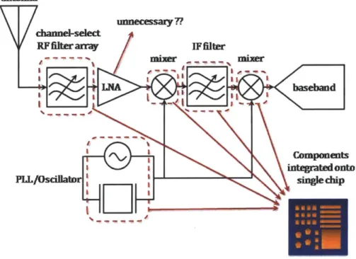
Currently, a larger proportion of cell phones use large passive mechanical components such as Surface Acoustic Wave (SAW) and Film Bulk Acoustic Resonator (FBAR) based technology which have seen very little miniaturization over the past few years and cannot be integrated into Silicon technology. For these, microelectromechanical resonators provide a low small size, integrable, low cost and low-power alternative which makes them attractive candidates which can keep pace with the miniaturization and integration trends of the wireless communication industry. This leads to the about the vision of a single integrated solution for radio components including RF and IF filters, mixers and oscillators onto a single chip as shown in Figure [1.1].
Similarly, in microprocessor technology, small-size Silicon-based electromechanical resonators can provide synchronized low power clocking arrays with reduced jitter and skew, allowing the technology to
scale to high frequencies with high-precision clocking.
1.2 Types of MEMS Resonators
Since the demonstration of the first resonant structure in the form of the Resonant Gate Transistor by Nathanson in 1967 [1] MEMS-based resonating structures have been designed in a variety of shapes and
forms. They operate in various resonant eigenmodes, including flexural, contour and longitudinal, and they may be actuated and sensed (i.e. transduced) in a variety of ways, some of the most prevalent ones
antenna
Figure 1.1: Vision for a single integrated solution for radio components employing multi-band filters, mixers and oscillators onto a single chip.
being capacitive, piezoelectric, thermal and optomechanical. This project pertains to longitudinal mode bulk acoustic wave resonators, so we will first go into the details of this particular mode. Similarly, from a transduction perspective, we will discuss the capacitive or dielectric based and piezoelectric mechanisms as they are most relevant to this project.
1.3 Mechanics of Vibration
We discuss the mechanics of the longitudinal bulk mode of vibrations of bars in order to better understand the resonant eigenmode of the device under consideration and set up the wave equation for the same.
Assuming we have a device with a resonant length L, operating in the nth mode of resonance given by frequency
fj
which corresponds to the angular frequency wn. The wavelength A, for the nth mode is give by:n
2 L and thus the wave number kn is given by
2 7r n 7r kn = - =
-k An L
The acoustic velocity, vel, in this device is given by
vel = F Peff
where Eeff and Peff are the effective Young's modulus and the density of the device. Using these, we have the resonant frequency given by:
vel n Ee5 n 7r E,5f
n eff _ w Eef n= 2wfn =2 = 2=--
An 2 L Peff L Peff
Using the above equations, we can now construct the wave equation for the modal shape for this device, modeling it as a lateral mode bar resonator:
u(x, t) = Uosin(knx) -ejont
Once the wave equation is set up, we may solve for the amplitude of vibrations using the equation for damped longitudinal vibrations in a bar. For a bar with cross sectional area A, and a driving stress function a7, this equation is given by:
a2u(x, t) du(x, t) A 2u(x, t) dadrive
at2
Atax2- eff ax2
dx
However, before we can use this equation to calculate the amplitude of vibrations, we need to calculate the damping coefficient b in terms of material properties and other measurable quantities.
We start by cancelling the term A throughout and substituting u(x, t) = U(t)sin(knx) into the beam equation, where U(t) = Uoeijnt. Thus we get:
2d' U(t)sin(kx) + 2a U(t)sin(knx) eU(t)sin(kx)
Perff2 at2 + " a
at
+ Eeffkn2 U-~i~kx = f (x, t)dx
We take the Laplace transform on both sides with respect to the variable t and set initial conditions of displacement and strain to zero. Let the Laplace transform of U(t)sin(knx) be denoted by U(x, s) and the Laplace transform of the RHS be denoted by F(x, s) to get:
U(X,S)[Peff S2 + bkn2S + Eeffkn2] = F(x, s)
This may be re-written as the transfer function H(s) given by: 1
U(x, s) _ Peff
(s) F(x,s) bk 2 Eeff kn2
Peff Peff
This is a second order system response, the denominator of which may be compared to the denominator of the second order harmonic oscillator response with Quality factor (Q) and an undamped resonant frequency, on, which is given by:
o2
H (s) =
s2 + Wn~-S + U)'2
Q
Equating the constant, we see thatE eff k 2
Peff
which is consistent with our equations and so we may equate the coefficient of the s term to get the damping coefficient b as:
bkn 2 _ _ kn Eeff
Peff
Q
Q
Peffb.-EeffPeff kn Q
1.4 Transduction Mechanisms
1.4.1 Dielectric or Capacitive Transduction
After a mechanical analysis of the resonator as a longitudinal mode bar resonator, we turn our attention towards driving and sensing this resonant mode.
One of the pioneering capacitive structures is the comb-drive resonator demonstrated by Tang et. al. in 1989 [2]. This comb drive resonator consisted of a large suspended structure with interdigitated fingers on its sides which would form capacitors with its surrounding anchored comb structure as shown in Figure[1.2 (a)].
Cross sectional F Vac
area A
(a) (b)
Figure 1.2: (a) Optical Micrograph of Comb drive [3] showing interdigitated fingers, (b) schematic of single capacitor driven with a DC bias V with small AC driving voltage vac
The air gap capacitors thus formed could be used to actuate the resonance of this proof mass suspended on beams using the capacitive force. Mathematically, for a capacitor structure in Figure [1.2 (b)] the capacitance C is given by:
C =O 9
For a DC bias voltage V + a small AC bias vacej"t applied across the plates, the energy E and the
capacitive force F are given by:
1. E =- C (V + vaceit)2 2 aE F =-au 13
d 1 e0 A = a(V
+
vacej" t 2 au 2 g + u 1 V2j, a E0 A =-(2 + 2Vva t+vc
2wt _ 2 aug+u -1 (V2 2 co) EA = -(V 2 + 2Vvacefto + Vace ) (g2(g+
u)
2We assume the displacement of the capacitor plates due to this force, x, is much smaller than the initial distance between the plates, g. We also see that the voltage term in the brackets has a DC component and AC components at a and 2a. Taking only the AC component at a into account, the force is given by:
EOA VveJ .
~ 2 ac
As discussed previously in Section [1.3], the displacement wave form for this resonator is given by:
u(x, t) = Uosin(knx) - ecnt
On the sensing side, we apply a DC bias voltage Von the capacitor plates to get an AC output current
aQ
ac
iout V
-a
1
= VE0 VEAatA
-g + u
Again assuming that the displacement, u «g,
=-VEAU
. V 0 A
-j~n 92 U(x) el~nt
where U(x) is the amplitude term dependent on the x coordinate of the capacitor plate with respect to the coordinate system.
Based on the above, one of the first improvements in capacitively transduced resonators came in the form of substituting a high-k dielectric film in place of the air gap in this capacitor [4], which boosted the force term as well as the output current term by the magnitude of the relative permittivity of the dielectric. This dramatically improved the transduction efficiency and reduced the motional impedance (R,) values of
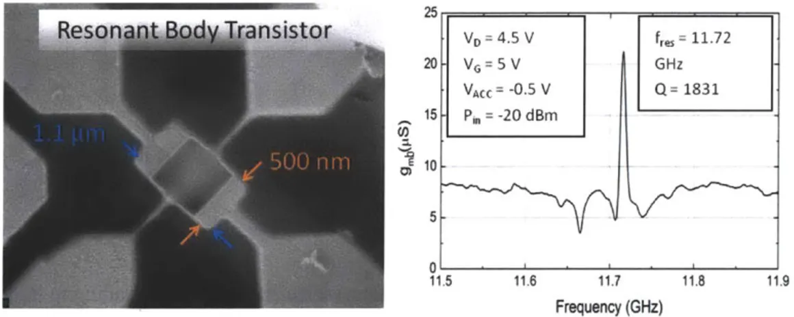
capacitive resonators by reducing the gap size. The next improvement came in terms of integrating the dielectric films inside the body of the resonator [5] which avoided the losses from acoustic energy leaking into the surrounding material through the dielectric films and allowed the more efficient mechanism of piezoresistive sensing to be employed in place of capacitive sensing, thus lowering the motional impedance further. Finally, the Resonant Body Transistor [6] or RBT shown in Figure [1.3], used these integrated dielectric films to create a transistor based resonators with high-k gate dielectrics for actuation and sensing which not only allowed for further reduced R, values but also showed promise for resonator frequency scaling with transistor technology.
25 VD = 4.5 V f.= 11.72 20- VG=5V GHz VAcC = -0.5 V Q= 1831 15 P= -20 dBm 10 5 0 11.5 11.6 11.7 11.8 11.9 Frequency (GHz)
Figure 1.3: (left) An image of the Resonant Body Transistor (right) along with its frequency response.
1.4.2 Piezoelectric Transduction
Piezoelectric transduction is one of the most efficient transduction mechanisms used in MEMS based resonators. The underlying principle used is the piezoelectric property of materials such as AlN. These materials develop a strain in their bulk in response to an applied electric field applied across them and vice-versa, electric charge is induced on the surface of these materials in response to a mechanical strain. The fundamental equations of piezoelectricity may be expressed in the following manner:
T =cS - eTE D = eS + EE
in which S is the strain matrix, T is the stress, c is the compliance matrix. E is the electric field applied externally and D is the electric displacement matrix. e and eT are the piezoelectric matrices (direct and transpose) and E is the dielectric matrix [7].
For a crystal with hexagonal symmetry such as AlN, this matrix assumes the following form: [8]
S
C11 c12 c1, 0 0 0 -S 0 0 e3, T, C11 C1 0 0 0 32 0 0 en --T,
c3 0 0 0 S3 0 0 e-3 ET4C
440
0
S
40
e2
40
T
C4 0 S5 e,5 0 0 _E 6c S 0 0 0 S D, El 0 0 E [ 0 0 0 0 e, 0 D, = 0O E, + 0 0 0 el, 0 0LD3
L6
1
3 Le
3, e3,e3
30
0
oJS4
S5 S6,Piezoelectric coupling coefficients are much stronger than dielectric coefficients leading to R, values of a few tens of Qs vs the kQ range values obtained for dielectric based resonators as shown in Figure [1.4]. The tradeoff is often the lowering of the quality factor (Q) which is intrinsically lower for the electrode material such as Molybdenum surrounding the piezoelectric materials [9] which form the bulk of these resonators. An effective solution was shown by Abdolvand et al [10] in terms of boosting both the power-handling and
Q
values of piezoelectric resonators by mounting them on a silicon substrate, with an inherently higher material limit on the quality factor. Techniques combining dielectric and piezoelectric sensing [11] have also addressed this issue but ultimately, the difficulty in integrating piezoelectric materials with silicon-based circuitry presents an inherent problem in scaling these devices to higher frequencies with transistor technology.4, 20621954MME.m de Q 25:5,2 Los 46727 dB
f ~
208
MHz
Rn,~
70D
Qunloaded
6,000
Figure 1.4: Frequency response (S2) of a Piezoelecric Resonator mounted on Silicon showing SEM of device used (inset) [10]
1.5 Electrostriction
Electrostriction is a property of insulators associated with randomly oriented domains within the material. In the presence of an electric field, these domains form localized polarizations which can attract each other, causing a strain to form in the material. Mathematically, electrostriction is defined as the quadratic coupling between strain (s) and electric field (E), or between strain and polarization (P). This is a fourth-rank tensor expressed by the following relationships
Sij = CEijklij + MijmnEmEn Sij
=C
ijklTij + QijmnpmPnUsing the second equation above, we see that for a piezoelectric film such as AlN, the strain along the direction i,
j
is defined as sij, is related to the Stress along that direction Tij, through the complianceC Pijk and to the polarization along the directions m and n, through the coefficient Qijmn .If we apply an
electric field in only one direction, say the c-axis of the piezoelectric material, the resultant electrostrictive stress, Gestric, will be expressed in terms of Epiezo , the Young's Modulus of the material
and S3 3, the strain along the c-axis as:
0
estric = Epiezo S33
This expands to:
Cestric = Epiezo Q3 3P3 2
Epiezo
Q
33E2 (kpiezo - ()Where E0 is the permittivity of free space, kpiezo, is the relative permittivity of the piezoelectric film of thickness g, and V is the voltage applied across it.
Electrostriction is usually a secondary mechanism used for actuating a MEMS resonator.
Keeping these mechanisms in mind, we now introduce the Piezoelectric Resonant Body Transistor proposed in this work.
THE PIEZOELECTRIC RESONANT BODY TRANSISTOR
2.1 Motivation
As transistor technology continues scaling to the deep submicron range driven by Moore's Law, transistor threshold frequencies have increased, enabling transceiver circuitry to be designed in the tens of GHz range. The released and unreleased resonant body transistors [6, 12] have been demonstrated as dielectric based, high
Q
components with high spectral purity that utilize the inherent gain of the field effect transistor for amplifying the mechanical resonance signal. However, the impedance of these devices is still orders of magnitude greater than those of piezoelectric devices. At the same time, devices using piezoelectric transduction [13, 14] have been demonstrated in the multi-GHz range with low impedance values due to the high coupling coefficients of piezoelectric materials. Combining the amplifying effects of FET sensing with the high transduction efficiency of piezoelectric materials suggests the design of the Piezoelectric Resonant Body Transistor.2.2 Principle of Operation
It is useful to discuss the basics of the Resonant Body Transistor (RBT) as a starting point for the Piezoelectric RBT as they share some common features. From the electrical point of view, the RBT is a two-gate transistor, with a dielectric such as Silicon Nitride or Hafnia in place of the gate oxide. The transistor is biased into saturation by tying the source to ground and applying a DC bias to the sensing gate and the drain. The back gate is also the actuation gate which is biased into accumulation. From a mechanical point of view, the RBT is a longitudinal mode bar resonator which is driven capacitively by applying a small AC bias to the back gate or actuation gate to launch acoustic waves into the device. The device resonates perpendicular to the direction of the channel. The resonance is sensed piezoresistively with a small capacitive contribution at the channel which is observed as a modulation in the transconductance.
The Piezoelectric RBT uses piezoelectric films in place of the gate oxide of the Dielectric RBT [Figure 2.1]. On the driving side, acoustic vibrations are now driven piezoelectrically, through the e33 coupling coefficient resulting in a higher driving stress and larger amplitude of vibrations. On the sensing side, the piezoelectric film experiences strain due to the longitudinal vibrations in the bar at resonance, and this results in a modulation in the polarization and hence electric field across the film through the inverse piezoelectric coefficient. This is modeled as a modulation in net gate voltage and is usually the dominant term over piezoresistive and capacitive contribution. The full analytical model for the device is discussed below. W i A -L/2 x=0 L/2 L IHf
~
A 'A' A'(a)
(b)
Figure 2.1: (a) Schematic of piezoelectrically transduced Resonant Body transistor. AIN piezoelectric films are used in place of the gate oxide for a double-gate transistor for sensing and actuation. (b) Cross section along A-A' line.
2.1 Table of Parameters
Parameter Description
L Length of Device along resonant dimension W Width of device, along direction of channel
H Thickness of device, determined by thickness of device layer on SOI wafer
VD
Drain Voltage
VA Back-gate DC voltage
Vac Back-gate AC voltage
g Thickness of Piezoelectric film
e33 Piezoelectric coefficient along c-axis
Q33
Electrostrictive Coefficient of piezoelectricn Number of harmonic
fA
Frequency of operation at nth harmonicUO Amplitude of vibrations
d Center-to-center distance between piezoelectric films Ex Young's modulus of material x along resonant dimension p Density of material x
LMO Length of Mo electrode along resonant dimension
Q
Quality factor of device at frequency fsO Permittivity of free space
kpiezo Relative permittivity of piezoelectric material Lgate Length of gate
yn Electron mobility in channel VT Threshold Voltage
ksi Relative Permittivity of Si
q Elementary Charge
NA Doping of the device body
k Boltzmann Constant
T Temperature of operation
ni Intrinsic Carrier Concentration in Si
Qpiezo Induced sheet charge in channel due to piezoelectric effect Vpiezo Induced voltage on gate due to piezoelectric effect
2.3 Driving of Acoustic Vibrations 2.3.1 Piezoelectric Contribution
The device is operated as a transistor by biasing the source at ground and applying a DC voltage VD to the drain and a DC voltage VG to the sensing gate. The back gate or driving gate of the piezoelectric RBT is biased into accumulation by applying a DC voltage VA. We then apply a small AC voltage Vaceilnt to the drive gate, in addition to VA, to launch acoustic waves into the device. Thus, the net voltage applied across the back gate is VA + vace"nt on the source side and VA + vaceint - VD on the drain side. This results in an average driving voltage of
VA + vaceI""nt _ VD 2
and an average value for the electric field across the piezoelectric film of thickness g is VA + vacelnt _ VD
2g
Using the Piezoelectric equations discussed previously, the resultant in-plane stress in the piezoelectric film, apiezo, along the direction of the Electric field, which is also along the direction of the c-axis given by
VA + vace'"Ot - VD VA- VD + vacejOnt
apiezo = 3 3 3 3
Hence the AC stress, 3p, relevant for the amplitude of vibration calculation, is given by
vaceiOnt
FP -e 33 2 g
2.3.2 Electrostrictive Contribution
In addition to the piezoelectric effect, electrostriction also contributes to stress in the AlN. As discussed in section [1.5], the stress is induced due to electrostriction, aYestric, given by:
2 (VA - D + vacejOnt2 Gestric = Epiezo Q3 3Eo (kpiezo - 1) (
-2(2
= Epiezo Q33
2
kpiezo-)((VA
- VD)2
+
2(VA
- VD)vacejI'nt + vac2jontIgnoring the DC component and the component at frequency 2wn, we have the AC component of the electrostrictive stress given by:
Epiezo
Q33E2 (kpiezo - 1) (Ge 0 2 (VA - VD)vaceant
2 g2
Thus, the total driving stress will be adrive = (Yp + (e
2.4 Analyzing the waveform 2.4.1 The Resonant frequency
As discussed in section [1.3], we can now construct the wave equation for the modal shape for this device, modeling it as a lateral mode bar resonator:
u(x, t) = Uosin(knx) -ej&nt
where UO is the amplitude of vibrations and the wave number, kn, for the nth harmonic is given by
2
n n 7kn = -
=-/In L
and the resonant frequency, On, given by:
fl7r JEff
Wn E
L Peff
where Eeff and Peff are the effective Young's modulus and the density of the device. In this case however, it is more straightforward to calculate the frequency using the method of fractional wavelengths than through the calculation of the above. For this, we note that at resonance, for a standing wave to be formed in the resonator, we have
L= n 2
As the resonator is made up for a stack of materials with different acoustic velocities, for a resonant frequency
fn the acoustic wavelength corresponding to a material is given by
= vel,
fn
Thus in the Moly electrodes, this wavelength would be given by:
MO -velMo _ 1 EMO
fn n PMo
Similarly, we may determine the acoustic wavelengths in each of the films using the Young's moduli, E, of and density, p, of the constituent materials, Si for Silicon, piezo for the piezoelectric film and Mo for the Molybdenum electrodes. Now due to condition of forming a standing wave at resonance, we require that the total length is a multiple of a half-wavelength. Since the wavelength in each material is different, we may say instead that the sum of fractional wavelengths in each material constituting the resonator has to be a multiple of %. This may be expressed as:
2 LMO 2 Lpiezo Lsi n
AMO
Apiezo
ASi
2Substituting for the expression for the wavelengths, we have
2 LMO 2 Lpiezo Lsi n
fn + + -
=-Epiezo
o LPpiezo
]+
Mo E piezo Lsi
Ppiezo
2.4.2 Eef and pef
We now calculate Eeff and Peff, the effective Young's modulus and the density of the device. To find the values of these constants, we first observe that the vibrations happen along X axis, which consists of a 5-film stack [Figure 2.1b]. These five films may be considered to be five springs vibrating in series in
response to a bulk acoustic wave. We can assume each of these films to be a cuboidal bar and calculate the spring constant for the same. For such a bar with length 1, and cross sectional area w X h, the spring constant kbar for a force along the length 1, is given by:
E w h
kbar - 1
Thus, in this case, for the Moly film, with Young;s modulus EmO, the spring constant kmO will be
_Eo W H
kMG - LM
Similarly, we write the spring constant for the other films as well. We also write the effective spring constant, keff, using the effective resonant length of the device, which is just L as
k Eeff W H
keff= L
For these five springs vibrating in series, we now relate the individual spring constants to the effective spring constant as:
1~ 1
keff k
L 2 LMO 2 Lpiezo + _Lsi
Eeff W H Emo WH Epiezo W H Est WH Canceling the common terms and rearranging we get,
L
Feff 2 LMO
+
2 Lpiezo LsiEMo Epiezo
Esi
Using the above value, we now calculate the effective density using the relation
()n n T Eeff
2 7 2 7 L Peff
2.4.3 Amplitude of Vibrations
We use the equation for damped vibrations in a bar (1 D) to solve for the amplitude of vibrations:
d
2u(x, t) -
3u(x, t)
0
2u(x, t)
dadriveell t2Eef dx2
=
A
dx where the damping coefficient, b, is as calculated in Section [1.3] to be:b Eeff Peff
knQ
Canceling the cross section area term A, substituting u(x, t) = Uosin(knx) -eimnt and adrive = ap into the above we have,
-Peff wn 2ejunt Uosin(knx) +
jbwneiwntkn
2 Uosin(knx) + Eeffeiwntkn 2 Uosin(knx) = dxwhich may be rewritten as
da5drive
Uosin(knx) = dx
(-pPeffrnzei(nt + jbwneiwntkn2
+ Eeff eiontkn2
The driving stress due to the piezoelectric film is a constant value through the thickness of the piezoelectric film, g, and zero elsewhere. Thus, the slope of the driving stress [15], may be represented as delta functions at interfaces of the piezoelectric film which is sandwiched between the Silicon body and the Moly back gate. As per our x-axis convention given in Figure [2.1] is the piezoelectric film extends
from x c (d - , d + 2 on the drive side. Thus we have, dadrive = adrive (x -
(d
-6
(x -(d
+
]Substituting this into the above equation, multiplying both sides by sin(kx) and integrating from -L/2 to L/2 gives us:
L/2 f L/2 p [6 (x - (d - - 6 (x - (d + sin(knx) dx
Uo sm/ 2((kntx)dx = 2)n 2 2
)
UO = 2+drive + 2) sin knd kng - sin knd + kng
L eiwnt(_peff n 2 + jbOnkn2 + Ee kn \ 2 2
Reducing the second bracket using the trigonometric identity
(A -B) (A +B) sin A - sin B = 2 sin o s 2
2 2
we get,
sin knd - k)- sin knd + k)= - 2 sin kf) cos (knd)
Thus, substituting this into Uo we get,
UO = = 2Gdrive sin (kng cos (knd)
L efOnt (Peff(n2 + jbOnkn2
+ Eeffkn2
)
\212.5 Sensing of Acoustic Vibrations
2.5.1 Assumptions for Sensing Side: [16]
1. The mobility in the channel is independent of electric field, velocity of electrons is directly proportional to E-field.
2. The gradual channel approximation holds - Gate field (perpendicular to the channel) is much greater than drift field (parallel to current flow).
3. Sheet Charge Approximation holds -All inversion electrons are assumed to be in a very thin layer at the AlN-Si interface as compared to the thickness of the bulk or the Piezoelectric film.
4. Semiconductor surface not biased into degeneracy.
5. All of the bulk is uniformly doped and fully depleted.
6. Diffusion currents are negligible with respect to drift currents. 7. Surface state charge per unit area is constant.
9. Surface state charge is zero.
10. The channel is "long", no short channel effects are accounted for.
11. Sub-threshold current is negligible and the transistor is off at that point for all calculations.
2.5.2 Calculation of DC current
When all the above assumptions hold, the DC current in a field effect transistor whose source is tied to ground and the gate is biased at VGS and drain is biased at VDS , with a threshold voltage VT, is given by two simple relations. In the linear regime, when VDs VGS - VT, we have the current IDCLin given as
H VDS
IDCLin = L pnCpiezo(VGS - VT - S
Lgate2
In the saturation regime we have VDS VG - VT, and the current IDcsat is given by
H
IDCsat = 2 Le nCpiezo(VGS - VT) 2
2 gate
2.5.3 Calculation of Threshold Voltage [171
a ) For "long" bulk (i.e. maximum depletion region achieved)
In this case, the threshold Voltage, VT,is calculated using the formula:
VT = +
#sth
+ Qms dmax piezowhere the difference in work functions
#,s
between the body and the electrode material, also known as the flatband voltageOms
WSi
-WMoly
q
where the subthreshold voltage is given by
#Pstfwhere
q is elementary charge, , k is the Boltzmann constant, T is the temperature, NA is the doping of the bulk Silicon region and ni is the intrinsic carrier densityPsth = 2 k T (NA
q ni
The depletion charge at maximum depletion width is given by Qdmax, where esi is the permittivity of Silicon
Qdmax = V2 esi q NA
psth
b) For "short" bulk (i.e. fully depleted)
As the bulk of the device is quite short, it is fully depleted before the maximum possible depletion depth is achieved. Hence the threshold voltage occurs when the device reaches its maximum depth of depletion layer, following which it goes into inversion. In this case, the threshold voltage is given by:
V7 = @ms + (PS + Qdep
Cpiezo
In this scenario, the depletion charge, Qdep, is given by
Qdep = q N(2d - g)
The surface potential, which is obtained by integrating the charge Qdep over the depletion region, which is the entire length of the Silicon layer, to obtain the E-field, which is then integrated to obtain the potential at the surface
q NA(2d - g)2
(PS 2 Esi
where
#bg
is the surface potential at the back gate and is itself dependent on the back gate voltage. This is responsible for the feed-through and we will ignore the AC modulation for now and calculate the surface potential at the back gate for the DC bias VA.-2 k T pn s - VA
#e9 = qn
1
Y = C 2ESjqN
Cpiezo
2.5.4 Piezoelectric Contribution [161
In a hexagonal crystal such as AIN, for an externally applied field E3, dielectric constant, E3, direct
piezoelectric coefficient matrix given by e and the inverse piezoelectric coefficient matrix given by d (as discussed in the previous section) and strain given by S, the electric displacement vector D3 is given by
D3 = E3E 3
+
d31(S1 + S2) + d33S3 = E3E3 + e31(S1 + S2) + e33S3Assuming that the 1 -D standing wave at resonance, u(x, t), is only along the x direction which is also the direction along which the c-axis is oriented and the 33 coefficient is relevant, i.e. assuming that there is no strain along other two directions (Si = S2 = 0). Thus we can rewrite above as
D3= E3E3 + d3 3S3
Since the contribution of the externally applied electric field is already accounted for as the term VGS in the DC current equation for the sensing side, we set E3 = 0 and we write
D3
=
e33S3From this expression for the electric displacement, we may calculate the equivalent piezoelectrically induced Electric field, Epiezo and the corresponding voltage across the piezoelectric film, Vpiezo as:
f-d+g/2 r3 +9 Vpiezo
=
Epiezo(x)dx
=J
S3 (x)dx
d-g|2 E3 -2 e3 3 d+Bu(x, t) Vpiezo = - 3 - a ( t x E3 -d-ax
2 = eUosin(knx) -
eilntVpiezo =- Ujsin(kn(-d +- sin
(kn(-d
- ] eiwnt3 reducing(the 2i
sin A - sin B = 2 sin (A B)
2sn 2 2
we get,
sin (-kd + -) - sin (-kd = 2 sin (kfl) cos (kad)
2 -kd--22
Thus,
Vpiezo = -2!-3 UO cos(knd) sin (kn g)- eIjnt
E3 2
The transistor current in the linear regime, IDCLin and in saturation, IDCsat , as seen in the previous section is given by: H VDS IDCLin L E-nCpiezo(VGS - VT - VDS Lgate 2 H 'DCsat - npiezo GS T 2 2 Lgate
Thus the Vpiezo term simply contributes to an additional AC voltage on the sensing gate. Thus, in the linear regime, as long as the linear regime condition is satisfied with the net gate voltage (VDS 5 VG +
Vpiezo - VT) we can write the net current as a sum of the DC current, IDCLin, and an AC component,
1
pelec, as
H VDS
IDCLin + ipeleclin L E nCpiezo(VGS + Vpiezo - VT - VDS
gate 2
DCLin Lgate nCpiezoVpiezoVDS
H t peleclin a YnCpiezoVDSVpiezo Lgate H VDS Vpiezo -nCpiezo(VGS VT VDS Lgqate 2 (VGS - T ~ D
This may be expressed in terms of the DC linear regime current as:
tpeleclin = IDCLin Vpiezo
Similarly, in the saturation regime, (VDS VG + Vpiezo - VT)
IDCsat + ipelecsat 2 H PnCpiezo (VGS + Vpiezo - T
2
LgateH H
=DCsat +
H
lnCpiezoVpiezo(VGS - VT) + nCpiezoVpiezo2Lgate gate H H tpelecsat L EInCpiezoVpiezo(VGS - VT) + MnCpiezoVpiezo2 Lgate
2
Lgate H H V Y 2 2 n-piezo(VGS L VT 2 piezoT +l 2gat T- (VGSez(V VT(Vgt
~~izoVS-V)
i+L(Vate
EGS
~ VT)2This may be expressed in terms of the DC saturation current as:
2
Vpiezo Vpiezo2 tpelecsat = IDCsat G +
\GS _ VT) (VGS - T)2]
2.5.5 Piezoresistive Contribution
The standing wave along the x-direction in the resonator results in a time-dependent strain along the channel which modulates the mobility due to the piezoresistive effect [18]. From the previous section, we may express this as:
d _ 1 1 1 ESi S3(X)|x _d+ = rT
1 1 1 ESi kn Uocos
-knd
+in 2 2
In the linear regime, we have,
IDCLin + ipreslin H (Yn + d[n)Cpiezo VGS - VT - VDS
Lgate 2)
Lgate npiezo (VGS T 2 VDS (1 + Rn
-DClin + IDClin
Rn
t
preslin = IDClin = IDCLinW111 ESi knUOcos -knd +
Rn
2t
pressat = IDCsat A ~in IDCsat 7T111 Est kn UOcos knd +
The sign of the piezoresistive coefficient along the direction of the current determines whether this contribution is in phase or out of phase with the piezoelectric contribution.
2.5.6 Capacitive Contribution
Apart from the piezoelectric contribution to the output AC current, we will also have an AC current resulting from the change in the capacitance of the piezoelectric film. The insulating AlN film forms a capacitor which squeezes and expands due to the acoustic wave, and this results in an additional AC current. Thus, this current is positive when the capacitance increases, i.e. when the piezoelectric film is compressed. Calculating the capacitance at DC, Cpiezo, and at the maximum amplitude of resonance,
C'piezo, where the piezoelectric film expands to thickness g + Ag, we have,
Cpiezo - kpiezo
g
CIpiezo - E0 kpiezo
g + Ag
Thus, the change in capacitance, ACpiezo, assuming Ag is small, is given by:
ACpz = C' - C eo k piezo E0 kpiezo EO kpiezo Ag 0 kpiezo6g
piezo
Piezo
gpiezo g+ A g + Ag gWe now calculate the net increase in the thickness of the piezoelectric film, Ag, by integrating the strain function over the thickness of the film
-2+du(x) -d+g
Ag= dx = Uoeiwntsin(knx)| 2
_adx -a-9
21- 2
A g
=Uoeint
Isin (k(-d +
-sin
kn
(-d
.(A -B) (A +B)
sin A - sin B = 2 sin 2 s 2
2 2 we get, sin (-kd +
-Skg
2
kng sin (-kd - kjg)=2
2 sin2
cos (knd) Thus we get,Ag = 2 Uoelwnt sin cos (knd)
2
ACpiezo = 2 ezo Uoeint sin k2g) cos (knd)
In the linear regime, we have,
IDCLin + icaplin H Pn(Cpiezo +
ACpiezo)
(vGS - VT -YD)
VDS LgateLH nCpiezo(GS ~ T DS)DS (1+ I Cpiezo
Lgate Cpiezo
IDClin + IDClin
ACpiezo
Cp iezo
icaplin = IDClin Cpiezo Cpiezo
2 Dl kpiezo
ent
SinIDClin 2 Uew I-I) cos(knd)
Similarly in the saturation regime,
ACpiezo_
capsat = DCsat -piezo
Cpiezo
DCsat 2 EO piezo Uoejnt sin
9 (kng cos(knd)
The total modulation current in the linear or the saturation regime is thus given by summing these three contributions in that regime:
rout = tpelec + ipres + icap
Now that we have completed the full analysis for this device, we will look at the relative contributions of different mechanisms to the drive and sense side. This will help characterize and optimize the performance of the device.
OPTIMIZATION
3.1 Assumed Values
Given the set of equations in the previous section, we can make calculations regarding the expected performance of the piezoelectric RBT. For this, we assume the following default values for the device.
3.1 Table of Assumed Constants [7, 8, 17, 18, 19, 201
Parameter Value VD 1V VG 5V VA -5V
Vac
0.1 V
S10- 7 m or 100 nm Q33 0.92 m4/C 2 Esi 170 * 10' N/m 2 Epiezo 135* 109
N/m 2 EMo 329 * 109 N/m 2 LMo 2 * 10-7 m or 200 nm psi 2330 kg/m 3priezo
3200 kg/m 3 PMO 10280 kg/m 3 E0 8.85 * 10-12 F/m kpiezo 8.9 Lgate 500 nm H lum W Lgate + 2mpn
100*
10-4 V/m 2s 'ESj 11.6 q 1.6* 10-19C NA 102 0 /m3 k 1.38 * 10- 2 3J/K T 300K ni 1.08 * 1016/M 3 711 45 * 10-1 1M2/NQ
1000Piezoelectric Coefficients for AIN [7] e= 0
[
0 -0.58 -d= 109[
0-1.98
0 0 0.58 1 0 0 -1.98 0 0 .55 0 0 4 0 -0.48 0 0 -4 0 -0.48 00
0
(C/mA2) 0 0] 0110-1(C/N) 0 -4 0 0 3.2 Driving SideUsing the values from Table [3.1], the relative amplitude of the piezoelectric and electrostrictive stress (AC) is given by:
oTp _e
3 3g 2
Ge
Epiezo Q33E (kiezo 1)(VA-
VD)Thus the piezoelectric stress is more than two orders of magnitude greater than that due to electrostriction hence the latter will be ignored in subsequent analysis.
Using the piezoelectric-only drive, we get the following plot [Figure 3.1] for the gate voltage induced due to the piezoelectric film, Vriezo, with respect to time during one time period.
1.51 0.5--0.5-~ - -0.5 1 1.5 2 2.5 3 Time in seconds x 10-1
Figure 3.1 Plot of piezoelectrically induced voltage Vpiezo vs one time period
3.3 Sensing Side
The plot shows that the induced voltage varies between -lV and IV for default values. For a gate voltage of 5V, threshold voltage < IV and drain voltage of IV, this also means that the transistor is always in saturation for these default values. In this case, on the sensing side, we have the relative magnitude of the piezoelectric and the piezoresistive contribution in saturation given by:
(
Vpiezo Vpiezo2+12 ipressat 71x1
ES
kUocoS
(-knd+
k9In the linear regime, the relative amplitude is given by: Vpiezo
t
peleclin _ (VGS - VT -t
preslin r111 ESi kn Uocos
-knd +
and the relative magnitude depends on the values set for VGS and VDS. Thus for now we say that both the piezoelectric and piezoresistive effects have a non-negligible contribution to the output current.
The relative magnitude of the piezoresistive and the capacitive contribution in the saturation as well as the linear regimes are given by:
ie 1pres -2 111 Ei kn COS (knd +
10s
icap 2
E0piezo Sin (kg) cos (knd)
Thus we can ignore the capacitive contribution while setting up the equations on the sensing side.
3.4 Equivalent Circuit Model
With the above analysis in place, we can finally draw and equivalent circuit model of the Piezoelectric RBT which is based on the 7 model used for transistor analysis [Figure 3.2]. For the piezoelectric RBT, we modify the traditional model by introducing the acoustic transconductance I9ma which gives rise to a
high-Q voltage-dependent current source controlled by the driving gate voltage.
G
Cgd
D
p0
0
- - - ro Cds Cad-cgs Cgb mivgS gmnbs gmavbs -0 +T
C(small)
rCsb
lorenzian
B O
Figure 3.2: Equivalent circuit model for Piezoelectric RBT showing the gate (G), drain (D), source (S) and back gate (B) terminals, capacitances (C) and voltage dependent current sources with transconductance (g).
We may express this transconductance, gima, or the equivalent resistance at resonance, Rx, in terms of the output current, iout and the driving voltage, vac as:
1 Vac
9ma Amplitude(iout)
3.5 Trends in iout
We set up equations to plot the total AC output current iout vs time. Two of the important control parameters are VGs and VDs and we first observe the effect of changing those on the AC output current.
In Figure [3.3] the non-linearity for small values of the gate voltage occurs because the net gate voltage, which is given by VGS + Vpiezo switches between saturation, linear and sub-threshold regimes. For the net gate voltage to be permanently in the saturation regime, we require, VGS - Vpiezo - VT > VDS. For a
threshold voltage VT = 0.7V, VDs = 1V, and Vpiezo = 1V, the DC gate bias VGs 2.7V which agrees
well with the plot. Higher gate bias voltages lead to larger AC output current as the DC bias current
-IDcsa t increases with VGS in saturation, and the piezoelectric contribution to the AC output current also increases linearly with VGS following the transistor equations:
H
IDCsat 2 Lgate lnCpiezo (VGS n ~ T)2
H H
t
pelecsat = - InCpiezoVpiezo(VGS ~ VT) + 2 L nCpiezoVpiezo
Lgate gate
150
Time in ps
Figure 3.3: Plot of iout vs time for varying gate bias voltage VGS showing non-linearity for small VGS.
Thus, the higher the gate voltage, the higher the DC as well as AC output current, which leads to a higher transconductance and lower insertion loss for the device. The upper limit on this is that a large VGS will lead to a large leakage current through the piezoelectric film and ultimately result in its breakdown.
We now plot the output current as a function of the drain voltage VDS as shown in Figure [3.4]. For small values of VDS (< 3.3V), the condition VGS - Vpiezo - VT > VDS is always true for the known values of the
VGS = SV, Vpiezo = 1V and VT = 0.7 V and the transistor remains in saturation and no dependence on
VDS is observed as expected from the transistor equations. For intermediate values of VDS (between 3.3 V
and 5.3 V), the transistor switches back and forth between the saturation and linear regimes when Vpiezo is near its peak values and a distortion in the output waveform is observed. For high values of VDS, the condition VGS - Vpiezo - VT <VDS is always true, pushing the transistor into the linear regime where the dominant component of the AC output current, ipeleclin, is dependent on VDS through the relation:
H ipeleclin Lgt - nCpiezoVDSVpiezo Lgate 0.8 08V DS = 0.5V 0.6 _ .. =1V ... VD = 2V 0.4 - .VDS = 3V ... V DS = 4V 0.2- V = 5v ..- V = 6V 0 V DS= 7V -0.2-0
-0.4--0.6
-
-0 50 100 150 200 250 Time in psFigure 3.4: Plot of i0
n,
vs time for varying drain-source voltage VDs showing non-linearity for large VDs.Thus, for a sinusoidally varying output AC current the transistor must remain in the saturation or linear regimes. However, for a fixed drain voltage, the piezoelectrically modulated AC current in the linear regime is smaller than that in the saturation regime if:
H H H
ipelecsat e InCpiezo Vpiezo (VGS - VT) + 2 lnCpiezoVpiezo > Lgate InCpiezoVDSVpiezo
Lgate 2LgateL
iff
(VGS (V~s ~ VT) -VT) + 2 >piezo >VDDS
From Figures [3.3] and [3.4], we conclude that the output signal may be maximized by applying high gate and drain voltages to the device, the tradeoff being the limitations imposed by the application.
We next plot the AC output current, iout as a function of the quality factor in Figure [3.5]. The increasing
amplitude of iout with
Q
can be explained by the fact that a largerQ
value means that the amplitude of vibrations at resonance is amplified more, leading to a larger iout due to both piezoelectric and piezoresistive effects. The plot however shows that the distortion of the output waveform from a sinusoidal also becomes more severe with increasingQ,
thus requiring a tradeoff to be considered for device design. The quality factor is a variable determined by anchor loss, thermoelastic damping and phonon-phonon scattering and can be improved by using optimal materials and improved fabrication techniques such as Molecular Beam Epitaxy [21, 22].0.1 1 8 0.08 -0.06 0. 04 0 o :: 0.04- 0.4 600 800 1000 1,200 1,400 Quality Factor (Q) Figure 3.5: Plot of iout vs time for varying Quality factor (Q)
![Figure 1.2: (a) Optical Micrograph of Comb drive [3] showing interdigitated fingers, (b) schematic of single capacitor driven with a DC bias V with small AC driving voltage vac](https://thumb-eu.123doks.com/thumbv2/123doknet/13950767.452301/13.918.212.691.464.661/figure-optical-micrograph-showing-interdigitated-fingers-schematic-capacitor.webp)
![Figure 1.4: Frequency response (S2) of a Piezoelecric Resonator mounted on Silicon showing SEM of device used (inset) [10]](https://thumb-eu.123doks.com/thumbv2/123doknet/13950767.452301/17.918.184.718.129.533/figure-frequency-response-piezoelecric-resonator-mounted-silicon-showing.webp)


