Efficient and Stable Inorganic Perovskite Solar Cells
Manufactured by Pulsed Flash Infrared Annealing
Sandy Sanchez, Neururer Christoph, Bernard Grobety, Nga Phung, Ullrich Steiner,
Michael Saliba,* and Antonio Abate*
approach to enhance the stability of the material under device working condition, i.e., light and thermal stress.[6,7] ABX
3 halide perovskites most commonly used in solar cells contain cesium, methylam-monium (MA) and formamidinium (FA) in the A site, Pb in the B, and Br and I in the X site of the crystalline lattice.[1,8–10] Compositions based on organic cations, such as MA and FA, can be prepared with a bandgap of around 1.5 eV, which is suited for an efficient single junction solar cell.[11] However, the presence of organic cations, and in particular the volatile MA, is linked to the relatively poor thermal sta-bility and the high sensitivity to humid air, which affect most of the perovskite compositions employed in highly efficient PSCs.[12–16]
Swapping entirely or in part the organic with inorganic cations, such as cesium (Cs), can help to enhance the stability of halide perovskites at the cost of a bandgap higher than 1.5,[17,18] which is suboptimal for a single junction solar cells. For example, the fully inor-ganic CsPbI3 perovskite has a bandgap of 1.7 eV, which is not optimal for single junction but is instead nearly ideally suited for perovskite–silicon tandem solar cell.[19–21] Unfortunately, CsPbI3 is only stable in the photovoltaic active perovskite struc-ture – black phase – at temperastruc-tures above 300 °C,[22–25] which is not useful for applications. Partially (or completely) replacing iodide (I) with bromide (Br), i.e., exploring CsPbIxBr(3−x) com-positions, can stabilize the active photovoltaic phase at room temperature with progressively increasing bandgap as the bromine content increases. This mixed halide approach is extensively used to prepared stable inorganic halide perovskite both for photo voltaic and light emitting devices.[26–32]
As restricted to photovoltaics, it is a challenge controlling the interplay between phase stability, which can be obtained by enhancing the Br content, while maintaining the smallest possible bandgap. Indeed, the larger ionic radius of I as com-pared to Br upsets the stability perovskite, which tends to relax in a photovoltaic inactive delta phase.[33–37] The I/Br ratio must be therefore adjusted to achieve the lowest possible bandgap without sacrificing the perovskite phase stability. In the search for the best I/Br ratio, CsPbI2Br (I 67%, Br 33%) has been so far indicated as the optimum to achieve the highest efficiency PSC with a stable inorganic perovskite.[34–38] Liu et al. reported
Organic–inorganic perovskite solar cells have achieved impressive power conversion efficiency over the past years, yet operational stability remains the key concern. One strategy to improve long-term stability is to replace the thermally unstable organic with inorganic cations comprising the perovskite lattice. Here, for the first time, pulsed infrared light is used to drive the crystallization of inorganic mixed halide CsPbIxBr(3−x) perovskite films in solar cells with a power conversion efficiency exceeding 10%. By varying the iodide–bromine ratio systematically, it is found that to keep the inorganic perovskite black phase stable at the room temperature, the iodine content needs to be limited to lower than 60% – bromine content higher than 40%. The finding revises previous reports claiming stable compositions with higher iodine contents, which is systematically exploited to reduce the perovskite bandgap with the aim to enlarge the light absorption spectra and thus to boost the device efficiency. It is demonstrated that the newly defined stable compositional range enables devices that retain 90% of the efficiency after stressing the perovskite at 200 °C for 1 h. This result demonstrates that inor-ganic halide perovskites are stable materials for high-temperature applica-tions such as concentrated photovoltaics.
S. Sanchez, Prof. U. Steiner, Dr. M. Saliba Adolphe Merkle Institute
Chemin des Verdiers 4, 1700 Fribourg, Switzerland E-mail: [email protected]
N. Christoph, Prof. B. Grobety Geoscience Department University of Fribourg
Chemin du Musée 6, 1700 Fribourg, Switzerland N. Phung, Dr. A. Abate
Helmholtz-Zentrum Berlin für Materialien und Energie Kekuléstraße 5, 12489 Berlin, Germany
E-mail: [email protected]
1. Introduction
Perovskite solar cells (PSCs) have shown impressive lab-scale efficiency gains in a few years. However, additional work is needed to deliver a viable PSC technology for large-scale production.[1–3] This work includes the device stability and the close related stability of the perovskite primarily as one of the materials comprising the device.[4,5] Tuning the chemical composition of the perovskite seems one of the most promising
http://doc.rero.ch
Published in "Advanced Energy Materials 8(30): 1802060, 2018"
which should be cited to refer to this work.
recently a record power conversion efficiency (PCE) of 12%[39] for PSCs using CsPbI2Br. Together with the latest work, most of the previous publications identified in I 67%, Br 33% the best halide composition.[40] We believe that many research groups ended up with the same I/Br ratio since it can be prepared straightforwardly by dissolving an equimolar amount of the two precursors PbI2 and CsBr in solution. Preparing different I/Br ratios requires at least three of the following precursors, PbI2, PbBr2, CsI, and CsBr, some of which are difficult to dissolve, imposing inconvenience during film preparation, and chal-lenging to process in a thin film to prepare PSCs.
In this work, we identify a window of compositions that revises previous reports, allowing bromine contents higher than 40% (iodine lower than 60%) in the preparation of stable inorganic mixed halide CsPbIxBr(3−x) perovskites. We make use of pulsed flash infrared annealing (p-FIRA) as a versatile new method to control the crystallization of inorganic perovskite films in solar cells with a PCE exceeding 10%. We prove the extraordinary thermal stability of inorganic perovskites reporting PSCs that retain 90% of the efficiency of a pristine perovskite film after heating for 1 h at 200 °C.
2. Results and Discussion
2.1. Stable Inorganic Perovskite Mixed Halide Composition
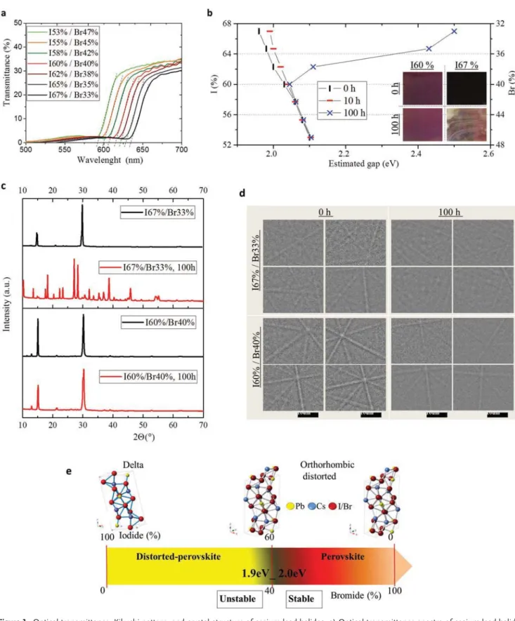
We prepared a library of mixed halide compositions of inor-ganic CsPbIxBr(3−x) perovskite films from a single solution of the three precursors CsBr, PbI2 and PbBr2, as detailed in the Experimental Section. Figure 1a shows the optical transmission spectra for perovskite films prepared from different composi-tions around 60% of iodine (40% of bromine, CsPbI1.8Br1.2). According to literature, increasing iodine content redshifts the absorption onset – lowers the bandgap. The plot in Figure 1b displays the bandgap estimated from the optical transmittance spectra as a function of the iodine content. The trend is linear for freshly made films as reported in the literature, however, after 100 h of storing in the dark with a relative humidity lower than 35%, all the samples with iodine content above 60% exhib-ited a marked blueshift of the bandgap. The change in bandgap was also obvious comparing by eye freshly made and 100 h old films (inset Figure 1b). Such a change is indicative of instability for the films prepared from the compositions with iodine con-tent higher than 60%.[41,42]
Cesium-based perovskites prepared from mixed halide com-positions adopt an orthorhombic crystal structure at room temperature.[43–45] However, for the pure iodide composition, the stable crystal structure below 300 °C is the “delta,” also called yellow-phase (see the Supporting Information), which is unsuited for photovoltaic.[37,45–47] Figure 1c shows the X-ray diffraction (XRD) pattern for samples with 60% and 67% iodide contents, where the two main peaks at 30 and 15 2θ are char-acteristic of the orthorhombic perovskite structure.[48–50] We reported additional compositions in the Supporting Informa-tion. The same Figure 1c displays the XRD pattern (red lines) for the same films left in the dark for about 100 h at room temperature and relative humidity lower than 38%. We can observe that while the pattern of the film I60%/Br40%
(CsPbI1.8Br1.2) remained substantially unchanged, the pat-tern of the film I67%/Br33% (CsPbI2Br) reported several new peaks that are indicative of a lower symmetry crystal structure. This result strides with the previous literature, which indicated CsPbIxBr(3−x) perovskites with iodine content higher than 60% as the path toward stable PSCs.
Electron backscattering diffraction (EBSD) was carried out to extract the Kikuchi patterns of the perovskite films as reported in Figure 1d. The contrast between the Kikuchi lines and the background provides a qualitative measurement of the crystal-linity of the film. The as-prepared I60%/Br40% (CsPbI1.8Br1.2) film shows a strong Kikuchi contrast, which is still well dis-cernible after 100 h. The I67%/Br33% (CsPbI2Br) sample, on the other hand, displays a weaker contrast at 0 h, which decays almost completely after 100 h. This trend indicates a stable and higher crystallinity of CsPbI1.8Br1.2. On the contrary, the pat-tern of CsPbI2Br is indicative of lower crystallinity that decays over time.[38]
We summarized the result of our finding in the schematic of Figure 1e. A boundary placed at 60% iodine/40% bromine interrupts the continuous line of iodine/bromine composi-tions. All the compositions with iodine content lower than 60% – bromine content higher than 40% – have a stable orthorhombic perovskite structure at room temperature. CsPbBr3 crystallizes in the orthorhombic (Pnma) space group, adopting a distorted perovskite structure, the distortion occurs through two successive phase transitions at 88 and 130 °C, transforming the crystal structure to tetragonal (P4/mbm) and
cubic (Pm−w).[51–53] All the compositions with bromine content lower than 40% – iodine higher than 60% – evolves toward the delta phase, which is characteristic of the 100% iodine composition. The phase stability sets the lower accessible bandgap for CsPbIxBr(3−x) perovskite to 1.9–2 eV. To support the phase stability finding, we made perovskite solar cells (see the Experimental Section for details) with halide compositions of I62%/Br38% and I65%/Br35%. After 100 h of storing devices in normal environment condition, they showed a loss in efficiency of 15% and 50%, respectively (Figure S2, Supporting Information).
2.2. Thermal Stability
In addition to the challenge of preparing a phase stable CsPbIxBr(3−x) perovskite, which we demonstrated for iodine content below 60%, the thermal stability[17,54,55] is a funda-mental requirement for PSC applications.[57,58] Standard ter-restrial solar cells working condition need for 85 °C stable materials and devices, but significantly higher temperature are required for applications such as concentrated photo-voltaics.[56] In Figure 2a, we compared inorganic perovskite comprising three different halide compositions, with an iodine content below 60%, with the most widely used hybrid organic-inorganic perovskites, i.e., the MA, FA mixed compo-sition MA0.15FA0.8Cs0.05PbI2.5Br0.5. All three inorganic perov-skite films maintained their color upon extended annealing at 200 °C, a temperature that is almost 3 times higher than standard solar cell operating temperatures. In contrast, the hybrid perovskite film rapidly changed color from black to a
Figure 1. Optical transmittance, Kikuchi pattern, and crystal structure of cesium lead halides. a) Optical transmittance spectra of cesium-lead-halide
thin films. b) Estimated bandgap from optical transmittance measurements determined from the intersection of the short-wavelength decay of the transmittance curve with the wavelength axis (dashed lines). The inset shows pictures of freshly prepared samples and after storing for 100 h under environmental conditions. c) XRD patterns of inorganic perovskites films with two iodide/bromide ratios, for freshly made samples and 100 h storing in the dark at a relative humidity of 30% at 25 °C. d) Kikuchi patterns are arising from electron backscattering diffraction of the inorganic perovskite film collected at 0 and 100 h storing in the dark at a relative humidity of 30% at 25 °C. e) Illustration depicting the perovskite crystal structure as a function of the iodine/bromine ratio.
yellow as soon as the temperature passes 100 °C.[16,57,58] The XRD patterns in Figure 2b support the stability of the inor-ganic perovskite showing that the main two peaks at 16° and 30° remain practically unchanged upon heating at 200 °C for 1 h. On the contrary, the XRD pattern proves that the hydride perovskite film degrades to PbI2, which suggest the complete loss of the organic component. Figure 2c shows the transmit-tance spectra of the inorganic perovskites before and after annealing. The absorption onset of each inorganic composition remains stable.
We explored the thermal degradation mechanisms of the hybrid and inorganic halide perovskite using thermogravi-metric analysis (TGA) and differential scanning calorim-etry (DSC).[56] Figure 3a shows the TGA weight losses curves of 3 inorganic and the hybrid perovskite compositions for a temperature ramped up to 600 °C at 0 °C min−1. The hybrid perovskite reported a clear weight loss at about 250 °C, followed by a plateau and a second marked weight loss at ≈400 °C.
We explained the two-stage process to the degradation of the organic cations (MA and FA) at around 300 °C followed by loss of halide above 400 °C.[10,57,59] As expected from the absence of the organic component, all the inorganic perovskite composi-tions reported a significant weight only after passing 400 °C.
To identify any thermally induced structural transitions of the inorganic compositions, we performed a DSC analysis as shown in Figure 3b. The curve for the iodide-rich stoichi-ometry (red line) exhibits an exothermic feature at ≈330 °C, which we attributed to the transition from orthorhombic to cubic perovskite structure as previously discussed.[24,37] The 50% I/Br perovskite composition also shows this transition, albeit less pronounced, while the bromine-rich material lacks completely of this feature, suggesting the most thermal stable chemical composition. Thermal decomposition of all the inor-ganic materials sets in well above 400 °C, starting from the less stable rich in iodide and finishing with the rich bromine composition.[6,60,61]
Figure 2. Behavior of inorganic and hybrid perovskite films at high temperatures. a) Pictures of inorganic and hybrid (organic/inorganic) perovskite films
annealed at different temperatures under dry conditions. b) XRD patterns of the same perovskite films photographed in (a). c) Optical transmittance spectra for inorganic perovskite films before and after annealing at 200 °C for 1 h.
2.3. Grain Size Tuning Using p-FIRA
Thermal annealing of films after preparation is typically used to influence film morphology. Since the PSC perfor-mance strongly depends on the structure and morphology of the perovskite layer, detailed annealing protocols, e.g., flash annealing, and prolonged heating steps often result in effi-ciency gains.[62,63] While the use of FIRA has been reported in our previous work,[64] prolonged annealing with high-intensity IR light may cause perovskite degradation. Here, we have modified the FIRA protocol using very short high-intensity IR pulses and optimized this protocol to obtain homogeneous compact inorganic perovskite films. Since perovskite crystalli-zation proceeds by nucleation and growth, the optimicrystalli-zation of the film morphology requires control over both the nucleation and growth processes. In a reasonably flat TiO2 layer nucleation causes the formation of surface islands which subsequently
grow and fuse.[65] Both the kinetic processes take place far from thermodynamic equilibrium and are affected by the heat flow. The p-FIRA method offers unprecedented control over the whole kinetic processes, dialing in, for example, the activation energy as a function of the irradiation time.[66]
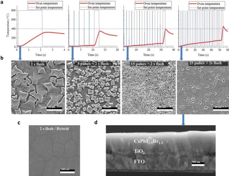
Figure 4a shows different pulse sequences consisting of
20 ms short flashes that are repeated 0–25 times, followed by a 2 s annealing pulse. The variation of the oven temperature measured with an infrared camera is also plotted. Figure 4b shows the resulting perovskite film morphology. With only the 2 s annealing pulse, the formation of ≈10 μm sized cuboids is observed. With the addition of 20 ms flashes, the cuboid shapes become more homogeneous, and the cuboid density increases with increasing flash number. This trend suggests that the flashes can initiate perovskite nucleation, multiplying the nuclei with each flash of an extended series of flashes. The longer annealing pulse is less effective in causing crystal nucle-ation, instead of enabling already nucleated crystals to grow. As evident from Figure 4b, a higher nucleation density ultimately results in more homogeneous films, rendering them nearly pinhole free when 25 flash pulses are used. Figure 4c shows in comparison a triple cation containing hybrid perovskite film resulting from a 2 s FIRA pulse, reproducing the large crystal domains that this system forms upon simple FIRA annealing, as previously reported.[64] A more detailed analysis of p-FIRA crystal formation is shown in the Supporting Information, also showing that film quality does not significantly change for more than ≈23 pulses. The cross-section of the 25-pulse sample in Figure 4d confirms the excellent homogeneity of this sample across the thickness of the perovskite film. Note that the overall irradiation process takes place in less than 50 s and stabilizes the perovskite phase without halide evaporation. The compactness of the 25-pulse film is a prerequisite for device manufacture.
2.4. Photovoltaic Performance and Stability
We used inorganic perovskite compositions CsPbIxBr(3−x) with x = 1.8 (I60%, Br40%), 1.5 (I50%, Br50%), and 1.2
(I40%, Br60%) to prepared PSCs as detailed in the Supporting Information. Figure 5a shows the current–voltage (JV) curves
of each champion devices for the three compositions and the PCE histogram for 10 devices for each composition. The com-position with the highest content of iodide enabled higher PCE devices, as expected from the smaller bandgap. The devices pre-pared with the bromine-richer perovskite reported the highest open-circuit voltage (Voc) value of 1.3 V consistent with the largest bandgap.[10] The external quantum efficiency (EQE) spec-trum collected for the champion device is reported in Figure 5b displaying a short-circuit current of 12 mA cm−2, which is close agreement with the value (12.3 mA cm−2) extracted from the JV curve in Figure 5a. The EQE plot also confirms a bandgap of roughly 2.0 eV (640 nm) for this particular halide composition.
The stability PSCs with the three stoichiometries were tested in two ways. The first batch of devices was irradiated for 1000 h with an AM1.5 spectrum under an inert atmosphere, followed by a JV measurement. In a second stability test,
the perovskite layers were annealed at 200 °C for 1 h before
Figure 3. Thermal study of perovskite films. a) Thermogravimetric
analysis (TGA) of hybrid and inorganic perovskite powders, scanned at 10 °C min−1. b) Differential scanning calorimetry (DSC) traces of
inorganic perovskite powders, scanned at 10 °C min−1.
finalizing the device manufacture with the deposition of the hole selective contact (poly(triarylamine) (PTAA), see the Exper-imental Section) and the gold contact. Figure 5c shows the PCE of freshly made (control) and stressed devices under light (100 h AM1.5) or high temperature (1 h at 200 °C), including the PCE distribution (box plot) for 5 independent devices pre-pared for each stoichiometry. Despite the harshness of the stability measurements, the PCE values deteriorated only by 10–16% compared to the control devices, with bromine-rich devices showing slightly higher stability (10–11% losses) com-pared to iodide-rich devices (13–16% losses). A comparison of the JV curves for 1000 h AM1.5 and 200 °C-annealed devices
made from the CsPbI1.5Br1.5 perovskite are shown in the Sup-porting Information.
Table 1 lists the champion device performance parameters
collected for each chemical composition. We observe that per-formance loss upon both light and thermal stress arises almost exclusively from a deterioration of the short-circuit current (Jsc), while the Voc and the fill factor (FF) remained unaffected or
they even improved. The light soaking experiment of 1000 h with an AM1.5 spectrum demonstrated the photostability of the optimized mixed halide inorganic perovskite. According to the report by Hoke et al., this result suggests the absence of halide segregation that may hamper the photostability of mixed halide perovskites.[67–69]
3. Conclusions
Our study demonstrates a new strategy to manufacture inor-ganic halide perovskites, paving the way for their use as efficient and thermally stable photovoltaic. We made use of p-FIRA to manufacture compact and pinhole free films of mixed halide CsPbIxBr(3−x) inorganic perovskites. We screened through the iodine/bromine mixed halide compositions with the aim to identify the most stable and effective material for solar cells. In contrast with past works, we found that a bromine content higher than 40% is needed to get a stable
Figure 4. Morphology comparison and cross-sectional images of perovskite films. a) Oven and set point temperatures for 4 different flash sequences.
b) Top view SEM images of CsPbI1.5Br1.5 samples annealed using the flash sequences of (a). c) Top view image of the MA-containing hybrid perovskite
film that was FIRA irradiated for 2 s. d) Cross-sectional image of the 25-pulse sample in (b).
perovskite phase. Thus, we used stable compositions to dem-onstrated perovskite solar cells with a power conversion effi-ciency exciding 10%. Most impressive, the devices retained 90% of their efficiency after heating the perovskite film at 200 °C for 1 h. This combination of thermal stability and device performance is unprecedented. This result demonstrates
the technological viability of perovskite for high-temperature applications such as concentrated photovoltaics.
4. Experimental Section
Photovoltaic devices were fabricated on fluorine doped tin oxide (FTO)-coated glass (Pilkington NSG TEC). The substrates were cleaned with Hellmanex soap, followed by 30 min sonication in a Hellmanex 2% water solution, 15 min sonication in isopropyl alcohol, and 5 min of oxygen plasma etching. Then, 30 nm thick TiO2 compact layers were deposited
onto the FTO by spray pyrolysis at 450 °C from a precursor solution of titanium diisopropoxide bis(acetylacetonate) in anhydrous ethanol and acetylacetonate. After spraying, the FTO substrates were left at 450 °C for 5 min before cooling to room temperature. Then, a mesoporous TiO2
layer was deposited by spin coating for 10 s at 4000 rpm with a ramp of 2000 rpm s−1, using a 30 nm particle size TiO2 paste (Dyesol 30 NR-D)
diluted in ethanol to achieve 150–200 nm thick mesoporous layers. After spin coating, the FTO substrates were dried at 100 °C for 10 min, and the films were annealed on a programmable hot plate (2000 W, Harry Gestigkeit GmbH) to crystallize TiO2 at 450 °C for 30 min under dry air flow. Li doping
of the mesoporous TiO2, as described elsewhere,[70] was accomplished
by spin coating a 0.1 M solution of bis(trifluoromethane)sulfonylimide lithium salt (Li-TFSI) in acetonitrile at 3000 rpm for 10 s followed by another sintering step at 450 °C for 30 min. After cooling down to 150 °C, all the substrates were kept on the fume hood (with relative humidity below to 38%) for the deposition of the perovskite films.
Figure 5. Performance and stability of PSCs prepared using 3 different inorganic compositions CsPbIxBr(3−x) with x = 1.8, 1.5, and 1.2. a) Current–voltage
(JV) curves of the champion device of each composition and the corresponding PCE histogram for 10 devices prepared identically. b) EQE of the device prepared using the champion composition CsPbI1.8Br1.2. c) PCE box plot comparing freshly made devices with devices stressed for 1000 h under AM1.5
light and devices fabricated from perovskite films thermally stressed for 1 h at 200 °C. Each box reports data collected from 5 independent devices. All JV curves were acquired in an ambient atmosphere with humidity around 35% using a slow voltage scan rate of 10 mV s−1 and AM1.5 simulated
solar light without preconditioning the device.
Table 1. Photovoltaic performance parameters collected from the
champion devices for control devices, 1000 h with an AM1.5 spectrum and 200 °C annealing for 1 h for each perovskite halide stoichiometry: CsPbI1.8Br1.2, CsPbI1.5Br1.5, and CsPbI1.2Br1.8.
Chem. Record values Voc [mV] Jsc [mA cm−2] FF [%] PCE [%]
I60% Br40% Control 1288 12.3 65 10.3 1000 h AM1.5 1287 10.9 66 9.2 1 h at 200 °C 1295 10.4 66 8.9 I50% Br50% Control 1282 11.0 65 9.1 1000 h AM1.5 1281 10.2 63 8.2 1 h at 200 °C 1294 9.1 66 7.8 I40% Br60% Control 1332 9.7 64 8.2 1000 h AM1.5 1291 8.5 68 7.5 1 h at 200 °C 1296 8.0 70 7.3
http://doc.rero.ch
Perovskite Solar Cell Preparation: The organic salts were purchased
from Dyesol; the cesium and lead compounds from TCI. The hybrid perovskite precursor solutions were deposited from a precursor solution containing CH5N2I (1 M), PbI2 (1.1 M), CH3NH3Br (0.2 M), and PbBr2
(0.2 M) in anhydrous dimethylformamide:dimethyl sulfoxide (DMSO) 4:1 v:v. Note that this composition contained a lead excess as reported elsewhere.[71] Then CsI, dissolved as a 1.5 M stock solution in DMSO,
was added to the mixed perovskite precursor to achieve the desired triple cation composition. The inorganic perovskite precursor solution was deposited from a precursor solution containing CsI (1.2 M), and to obtain the three final stoichiometries of CsPbIxBr(3−x), a variation of
PbI2 (0.2, 0.3, and 0.4 M) and PbBr2 (1, 0.9, and 0.8 M) for x = 1.2, x =
1.5, x = 1.8, respectively. To hybrid perovskite films, a hybrid-containing solution was spin-coated at 6000 rpm 20 s, and 100 μL of chlorobenzene antisolvent was poured onto the spinning substrate 5 s before the end of the program. The substrates were then annealed at 100 °C for 1 h in a nitrogen-filled glove box. After perovskite annealing, the substrates were cooled down within a few minutes. Perovskite films made by the FIRA included the spin coating of the perovskite solution in a single step at 4000 rpm for 10 s.[64] The substrates were then IR irradiated in
the FIRA oven, with 20 ms pulses from 0 to 25 and 2 s flashing and all the substrates were kept there for 10 s additionally before removal. The FIRA processing was carried out in a standard fume hood. Immediately after cooling the perovskite films, a PTAA (Merck) solution (35 × 10−3M
in toluene) was deposited by spin coating at 4000 rpm for 20 s. PTAA was doped with Li-TFSI (Sigma-Aldrich),) and 4-tert-butylpyridine (TBP, Sigma-Aldrich). The molar ratio of the additives to PTAA was: 0.0825 and 3.9 for Li-TFSI and TBP, respectively. Finally, an 80 nm thick gold top electrode was thermally evaporated under high vacuum.
Photovoltaic Device Testing: For photovoltaic measurements, a solar
simulator from ABET Technologies (Model 11016 Sun 2000) with a xenon arc lamp was used, and the solar cell response was recorded using a Metrohm PGSTAT302N Autolab. The intensity of the solar simulator was calibrated to 100 mW cm−2 using a silicon reference cell
from ReRa Solutions (KG5 filtered). JV curves were measured at reverse and forward bias at a scan rate of 10 mV s−1; this slow scan rate was
used in all JV measurements to minimize hysteresis effects. A shadow mask with a 0.1 cm2 aperture was used to define the active device area.
The EQE setup used was integrated inside the nitrogen-filled glove box with an inert atmosphere including an Oriel Instruments QEPVSI-b system, a Xenon arc lamp – Newport 300 W, a chopper (put at 35.5 Hz), and Newport Cornerstone 260 monochromator. A silicon diode was used to calibrate the lamp to subtract the background light noise. The monochromatic light spot was controlled such that the spot fit inside the active area of the device and the sample was ≈1.05 mm away from the light source. EQE measurements were carried out at short circuit.
Temperature Measurements: The temperature in the FIRA chamber
was measured using a K-type thermocouple connected to an Analog Devices AD595 amplifier interfaced with Labview software.
Material Characterization: Scanning electron microscopy and energy
dispersive X-ray spectroscopy were carried out on a Tescan MIRA 3 LMH with a field emission source operated at an acceleration voltage of 10 kV using an octane-pro energy dispersive X-ray spectroscopy detector. Electron backscattering diffraction was performed with HKL Advanced EBSD System using a Nordlys Nano Camera. Powder X-ray diffraction was performed in transmission geometry with Cu target (λ = 1.5401 Å) using an STOE STADI P diffractometer. Optical transmission measurements were performed using a Zeiss Axio-Scope A1 Pol using a Zeiss EC Epiplan-Apochromat 20 × objective and a xenon light source (Ocean Optics HPX-2000). For spectroscopic measurements, an optical fiber (QP230-2-XSR, 230 μm core) collected the light reflected from the sample. The spectra were recorded by a spectrometer (Ocean Optics Maya2000 Pro), and a standard white diffuser was used as a reference. DSC measurements were performed using a Mettler-Toledo STAR system under a N2 atmosphere. Experiments involving different heating and
cooling cycles were performed on ≈3 mg samples placed in standard DSC pans at 10 °C min−1. Thermogravimetric analysis for powder materials was
carried out in a PerkinElmer TGA 4000. 2–3 mg samples were placed in
ceramic pans, and the weight loss was monitored between 25 and 600 °C at a rate of 10 °C min−1 under a nitrogen flow rate of 20 mL min−1. Powder
samples were carefully scraped off the substrates right after annealing.
Supporting Information
Supporting Information is available from the Wiley Online Library or from the author.
Acknowledgements
M.S., U.S., and S.S. acknowledge the Adolphe Merkle and the Swiss National Science Foundation (Program NRP70 No. 153990).
Conflict of Interest
The authors declare no conflict of interest.
Keywords
inorganic perovskite, perovskite solar cells, pulsed flash infrared annealing, thermal stability
[1] M. Saliba, T. Matsui, K. Domanski, J.-Y. Seo, A. Ummadisingu, S. M. Zakeeruddin, J.-P. Correa-Baena, W. R. Tress, A. Abate, A. Hagfeldt, M. Grätzel, Science 2016, 354, 206.
[2] M. A. Green, A. Ho-Baillie, H. J. Snaith, Nat. Photonics 2014, 8, 506. [3] K. Domanski, B. Roose, T. Matsui, M. Saliba, S.-H. Turren-Cruz,
J.-P. Correa-Baena, C. R. Carmona, G. Richardson, J. M. Foster, F. De Angelis, J. M. Ball, A. Petrozza, N. Mine, M. K. Nazeeruddin, W. Tress, M. Gratzel, U. Steiner, A. Hagfeldt, A. Abate, Energy
Environ. Sci. 2017, 10, 604.
[4] M. Saliba, J.-P. Correa-Baena, M. Grätzel, A. Hagfeldt, A. Abate,
Angew. Chem., Int. Ed. 2018, 57, 2554.
[5] T. A. Berhe, W.-N. Su, C.-H. Chen, C.-J. Pan, J.-H. Cheng, H.-M. Chen, M.-C. Tsai, L.-Y. Chen, A. A. Dubale, B.-J. Hwang,
Energy Environ. Sci. 2016, 9, 323.
[6] Z. Wang, Z. Shi, T. Li, Y. Chen, W. Huang, Angew. Chem., Int. Ed.
2017, 56, 1190.
[7] M. Saliba, Science 2018, 359, 388.
[8] D. Bi, W. Tress, M. I. Dar, P. Gao, J. Luo, C. Renevier, K. Schenk, A. Abate, F. Giordano, J.-P. Correa Baena, J.-D. Decoppet, S. M. Zakeeruddin, M. K. Nazeeruddin, M. Grätzel, A. Hagfeldt, Sci.
Adv. 2016, 2, e1501170.
[9] N. Pellet, P. Gao, G. Gregori, T. Y. Yang, M. K. Nazeeruddin, J. Maier, M. Grätzel, Angew. Chem., Int. Ed. 2014, 53, 3151.
[10] N. J. Jeon, J. H. Noh, W. S. Yang, Y. C. Kim, S. Ryu, J. Seo, S. I. Seok,
Nature 2015, 517, 476.
[11] O. Grånäs, D. Vinichenko, E. Kaxiras, Sci. Rep. 2016, 6, 36108. [12] A. Calloni, A. Abate, G. Bussetti, G. Berti, R. Yivlialin, F. Ciccacci,
L. Duò, J. Phys. Chem. C 2015, 119, 21329.
[13] M. C. Harry, K. D. G. I. Jayawardena, S. Zlatka, S. Maxim, S. R. P. Silva, Nanotechnology 2017, 28, 114004.
[14] S. Bae, S. Kim, S.-W. Lee, K. J. Cho, S. Park, S. Lee, Y. Kang, H.-S. Lee, D. Kim, J. Phys. Chem. Lett. 2016, 7, 3091.
[15] A. Gomez, S. Sanchez, M. Campoy-Quiles, A. Abate, Nano Energy
2018, 45, 94.
[16] P. S. Whitfield, N. Herron, W. E. Guise, K. Page, Y. Q. Cheng, I. Milas, M. K. Crawford, Sci. Rep. 2016, 6, 35685.
[17] J.-P. Correa-Baena, M. Saliba, T. Buonassisi, M. Grätzel, A. Abate, W. Tress, A. Hagfeldt, Science 2017, 358, 739.
[18] G. E. Eperon, G. M. Paterno, R. J. Sutton, A. Zampetti, A. A. Haghighirad, F. Cacialli, H. J. Snaith, J. Mater. Chem. A 2015,
3, 19688.
[19] M. Lai, Q. Kong, C. G. Bischak, Y. Yu, L. Dou, S. W. Eaton, N. S. Ginsberg, P. Yang, Nano Res. 2017, 10, 1107.
[20] Y. Wang, X. Guan, D. Li, H.-C. Cheng, X. Duan, Z. Lin, X. Duan,
Nano Res. 2017, 10, 1223.
[21] D. P. McMeekin, G. Sadoughi, W. Rehman, G. E. Eperon, M. Saliba, M. T. Hörantner, A. Haghighirad, N. Sakai, L. Korte, B. Rech, M. B. Johnston, L. M. Herz, H. J. Snaith, Science 2016, 351, 151. [22] Z. Li, M. Yang, J.-S. Park, S.-H. Wei, J. J. Berry, K. Zhu, Chem. Mater.
2016, 28, 284.
[23] M. Pazoki, T. J. Jacobsson, A. Hagfeldt, G. Boschloo, T. Edvinsson,
Phys. Rev. B 2016, 93, 144105.
[24] O. Nazarenko, S. Yakunin, V. Morad, I. Cherniukh, M. V. Kovalenko,
NPG Asia Mater. 2017, 9, e373.
[25] T. Zhang, M. I. Dar, G. Li, F. Xu, N. Guo, M. Grätzel, Y. Zhao, Sci.
Adv. 2017, 3, e1700841.
[26] C. H. Ng, T. S. Ripolles, K. Hamada, S. H. Teo, H. N. Lim, J. Bisquert, S. Hayase, Sci. Rep. 2018, 8, 2482.
[27] B. C. Hames, R. S. Sanchez, A. Fakhar Uddin, I. Mora-Sero,
ChemPlusChem. 2018, 83, 294.
[28] A. Waleed, M. M. Tavakoli, L. Gu, S. Hussain, D. Zhang, S. Poddar, Z. Wang, R. Zhang, Z. Fan, Nano Lett. 2017, 17, 4951.
[29] Q. A. Akkerman, V. D’Innocenzo, S. Accornero, A. Scarpellini, A. Petrozza, M. Prato, L. Manna, J. Am. Chem. Soc. 2015, 137, 10276.
[30] Q. Ma, S. Huang, X. Wen, M. A. Green, A. W. Y. Ho-Baillie, Adv.
Energy Mater. 2016, 6, 1502202.
[31] X. Zhang, Z. Jin, J. Zhang, D. Bai, H. Bian, K. Wang, J. Sun, Q. Wang, S. F. Liu, ACS Appl. Mater. Interfaces 2018, 10, 7145. [32] D. Ghosh, M. Y. Ali, D. K. Chaudhary, S. Bhattacharyya, Sol. Energy
Mater. Sol. Cells 2018, 185, 28.
[33] S. Draguta, O. Sharia, S. J. Yoon, M. C. Brennan, Y. V. Morozov, J. S. Manser, P. V. Kamat, W. F. Schneider, M. Kuno, Nat. Commun.
2017, 8, 200.
[34] R. J. Sutton, G. E. Eperon, L. Miranda, E. S. Parrott, B. A. Kamino, J. B. Patel, M. T. Hörantner, M. B. Johnston, A. A. Haghighirad, D. T. Moore, H. J. Snaith, Adv. Energy Mater. 2016, 6, 1502458. [35] R. E. Beal, D. J. Slotcavage, T. Leijtens, A. R. Bowring, R. A. Belisle,
W. H. Nguyen, G. F. Burkhard, E. T. Hoke, M. D. McGehee, J. Phys.
Chem. Lett. 2016, 7, 746.
[36] R. Aso, D. Kan, Y. Shimakawa, H. Kurata, Sci. Rep. 2013, 3, 2214. [37] Y. Huang, W.-J. Yin, Y. He, J. Phys. Chem. C 2018, 122, 1345. [38] J. K. Nam, M. S. Jung, S. U. Chai, Y. J. Choi, D. Kim, J. H. Park,
J. Phys. Chem. Lett. 2017, 8, 2936.
[39] C. Liu, W. Li, C. Zhang, Y. Ma, J. Fan, Y. Mai, J. Am. Chem. Soc.
2018, 140, 3825.
[40] C. F. J. Lau, X. Deng, Q. Ma, J. Zheng, J. S. Yun, M. A. Green, S. Huang, A. W. Y. Ho-Baillie, ACS Energy Lett. 2016, 1, 573. [41] X. Tang, M. van den Berg, E. Gu, A. Horneber, G. J. Matt, A. Osvet,
A. J. Meixner, D. Zhang, C. J. Brabec, Nano Lett. 2018, 18, 2172. [42] G. F. Samu, C. Janáky, P. V. Kamat, ACS Energy Lett. 2017, 2, 1860. [43] P. Cottingham, R. L. Brutchey, Chem. Commun. 2016, 52, 5246.
[44] J. B. Hoffman, G. Zaiats, I. Wappes, P. V. Kamat, Chem. Mater.
2017, 29, 9767.
[45] R. J. Sutton, M. R. Filip, A. A. Haghighirad, N. Sakai, B. Wenger, F. Giustino, H. J. Snaith, ACS Energy Lett. 2018, 3, 1787.
[46] C. Yi, J. Luo, S. Meloni, A. Boziki, N. Ashari-Astani, C. Gratzel, S. M. Zakeeruddin, U. Rothlisberger, M. Gratzel, Energy Environ. Sci.
2016, 9, 656.
[47] F. El-Mellouhi, E. T. Bentria, S. N. Rashkeev, S. Kais, F. H. Alharbi,
Sci. Rep. 2016, 6, 30305.
[48] M. Shekhirev, J. Goza, J. D. Teeter, A. Lipatov, A. Sinitskii, J. Chem.
Educ. 2017, 94, 1150.
[49] Q. V. Le, J. B. Kim, S. Y. Kim, B. Lee, D. R. Lee, J. Phys. Chem. Lett.
2017, 8, 4140.
[50] L. Protesescu, S. Yakunin, M. I. Bodnarchuk, F. Krieg, R. Caputo, C. H. Hendon, R. X. Yang, A. Walsh, M. V. Kovalenko, Nano Lett.
2015, 15, 3692.
[51] C. K. MØLler, Nature 1958, 182, 1436.
[52] S. Hirotsu, J. Harada, M. Iizumi, K. Gesi, J. Phys. Soc. Jpn. 1974, 37, 1393.
[53] C. C. Stoumpos, C. D. Malliakas, J. A. Peters, Z. Liu, M. Sebastian, J. Im, T. C. Chasapis, A. C. Wibowo, D. Y. Chung, A. J. Freeman, B. W. Wessels, M. G. Kanatzidis, Cryst. Growth Des. 2013, 13, 2722. [54] G. Niu, X. Guo, L. Wang, J. Mater. Chem. A 2015, 3, 8970.
[55] T. Leijtens, G. E. Eperon, N. K. Noel, S. N. Habisreutinger, A. Petrozza, H. J. Snaith, Adv. Energy Mater. 2015, 5, 1500963. [56] G. Niu, W. Li, J. Li, X. Liang, L. Wang, RSC Adv. 2017, 7, 17473. [57] A. Dualeh, P. Gao, S. I. Seok, M. K. Nazeeruddin, M. Grätzel, Chem.
Mater. 2014, 26, 6160.
[58] N.-K. Kim, Y. H. Min, S. Noh, E. Cho, G. Jeong, M. Joo, S.-W. Ahn, J. S. Lee, S. Kim, K. Ihm, H. Ahn, Y. Kang, H.-S. Lee, D. Kim, Sci.
Rep. 2017, 7, 4645.
[59] T. Baikie, Y. Fang, J. M. Kadro, M. Schreyer, F. Wei, S. G. Mhaisalkar, M. Graetzel, T. J. White, J. Mater. Chem. A 2013, 1, 5628.
[60] J.-P. Correa-Baena, A. Abate, M. Saliba, W. Tress, T. Jesper Jacobsson, M. Gratzel, A. Hagfeldt, Energy Environ. Sci. 2017, 10, 710.
[61] Q. Ma, S. Huang, S. Chen, M. Zhang, C. F. J. Lau, M. N. Lockrey, H. K. Mulmudi, Y. Shan, J. Yao, J. Zheng, X. Deng, K. Catchpole, M. A. Green, A. W. Y. Ho-Baillie, J. Phys. Chem. C 2017, 121, 19642.
[62] M. Saliba, K. W. Tan, H. Sai, D. T. Moore, T. Scott, W. Zhang, L. A. Estroff, U. Wiesner, H. J. Snaith, J. Phys. Chem. C 2014, 118, 17171. [63] W. Nie, H. Tsai, R. Asadpour, J.-C. Blancon, A. J. Neukirch,
G. Gupta, J. J. Crochet, M. Chhowalla, S. Tretiak, M. A. Alam, H.-L. Wang, A. D. Mohite, Science 2015, 347, 522.
[64] S. Sanchez, X. Hua, N. Phung, U. Steiner, A. Abate, Adv. Energy
Mater. 2018, 8, 1702915.
[65] P. R. Willmott, in Pulsed Laser Deposition of Thin Films (Ed: G. K. Hubler), John Wiley & Sons, Inc., Hoboken, NJ 2006, pp. 633–648.
[66] I. Chorkendorff, J. W. Niemantsverdriet, in Concepts of Modern
Catalysis and Kinetics, Wiley-VCH Verlag GmbH & Co. KGaA,
Weinheim, Germany 2005, pp. 267–299.
[67] E. T. Hoke, D. J. Slotcavage, E. R. Dohner, A. R. Bowring, H. I. Karunadasa, M. D. McGehee, Chem. Sci. 2015, 6, 613.
[68] D. J. Slotcavage, H. I. Karunadasa, M. D. McGehee, ACS Energy
Lett. 2016, 1, 1199.
[69] M. C. Brennan, S. Draguta, P. V. Kamat, M. Kuno, ACS Energy Lett.
2018, 3, 204.
[70] T. Laird, Org. Process Res. Dev. 2002, 6, 201.
[71] M. Saliba, T. Matsui, J.-Y. Seo, K. Domanski, J.-P. Correa-Baena, M. K. Nazeeruddin, S. M. Zakeeruddin, W. Tress, A. Abate, A. Hagfeldt, M. Gratzel, Energy Environ. Sci. 2016, 9, 1989.