Design of Thermal Control Systems for Testing of
Electronics
by
Matthew Sweetland
B.S. Mechanical Engineering,
Purdue University (1993)
and
M.S. Mechanical Engineering,
Massachusetts Institute of Technology (1998)
Submitted to the Department of Mechanical Engineering
in partial fulfillment of the requirements for the degree of
Doctor of Philosophy in Mechanical Engineering
at the
MASSACHUSETTS INSTITUTE OF TECHNOLOGY
May 2001 Lvme 2# Vfl
@
Massachusetts Institute of Technology 2001. All rights reserved.
Author ...
...
Certified by.
BARKER
MASSACHUSETTS INSTITUTE OF TECHNOLOGY.JUL
1 6 2001
... ,LIBRARIESe of Mechanical Engineering
May 5, 2001
JohnH.... ...
John H. Lienhard V
Professor of Mechanical Engineering
Thesis Supervisor
Accepted by ...
Ain Sonin
Chairman of Graduate Studies
Department of Mechanical Engineering
Design of Thermal Control Systems for Testing of Electronics
by
Matthew Sweetland
Submitted to the Department of Mechanical Engineering on May 5, 2001, in partial fulfillment of the
requirements for the degree of
Doctor of Philosophy in Mechanical Engineering
Abstract
In the electronic component manufacturing industry, most components are subjected to a full functional test before they are sold. Depending on the type of components, these functional tests may be performed at room temperature, at cold temperature, or at high temperature (-500C to 1600C) depending on the type of component and intended market. The thermal management of these components during testing forms two basic issues that need to be addressed. The first issue is the heating or cooling of devices to the desired temperature prior to being tested, and the second issue concerns temperature control during the actual functional test.
This thesis covers the design, modeling and testing of two prototype systems. One system uses a low cost IR heating system to preheat bulk devices to a target tempera-ture, prior to the actual functional test. Theory shows that the limits on temperature ramp rates are imposed by the device package configuration and carrier configura-tion. The results from the prototype system show that the IR heating chamber is an effective low cost, low volume system for uniformly heating a wide range of device and carrier types.
The second prototype system uses high performance jet impingement coupled with laser heating to actively control the temperature of a high power density device during a functional test. Experimental results from the prototype system are presented and design guidelines for future systems are developed. The theory for temperature control is developed and the effects of package design and test sequence design on the temperature control limits are studied.
Thesis Supervisor: John H. Lienhard V Title: Professor of Mechanical Engineering Thesis Committee:
Prof. John Lienhard V Prof. Alex Slocum Prof. Bora Mikic
Acknowledgements
Needless to say, there are a large number of people that I wish to thank for assistance in the completion of this thesis and my doctoral degree. This project was sponsored by Teradyne Inc., and I wish to thank Andy Pfahnl and Ray Mirkhani at Teradyne for answering too many questions and for putting up with a very grumpy contract researcher. Pooya Tadayon at Intel has been very supportive with answers to technical questions about testing requirements and Intel provided the thermal test vehicles used in the prototype system. I want to thank the gracious patience of my thesis committee (John Lienhard, Alex Slocum, Bora Mikic, George Barbastathis) for putting up with way too many committee meetings in far too short of a period. My two advisors, John Lienhard and Alex Slocum, have been very helpful whenever I needed it, but also had the forebearance to leave me alone most of the time and allowed me to pursue the research as I found fit.
I also want to thank all my friends that have provided the necessary distractions over the past two years to prevent me from going nuts in the basement of MIT. Pat and Scott for the oversize trucks and water skiing. Millie and Buster for paddling, hiking and biking. All the others that suckered me into every possible sport requiring a helmet, body armor and/or enhance health insurance. I'm glad James was around for most of my stay. Always nice to have someone to bounce ideas off over a couple of beers (OK, so more than a couple). MJ and FB who provided the motivation to get done fast. Most of all I want to thank Virginie, who made the final year so much more bearable and enjoyable.
Contents
1 Introduction
2 Infrared Heating Theory
2.1 Radiant Heating . . . . 2.2 IR Heating Model . . . . 2.2.1 Component Heating . . . .
2.2.2 Device Modeling Results . . . . 2.2.3 Carrier Heating . . . . 2.2.4 Device/Component Coupling . 2.2.5 Degradation of Plastics . . . . . 3 Infrared Heating Experimental Results 3.1 Prototype Description . . . . 3.1.1 IR Source Selection . . . . 3.1.2 Heating Chamber Design . . . . 3.1.3 Carrier Holder and Mounting . 3.1.4 Instrumentation . . . . 3.2 Design Example . 3.2.1 Low Condu 3.2.2 High Cond 3.3 Experimental Data 3.4 Conclusion . . . . 3.4.1 Design Gui . . . . ctivity Carrier Design Example . dctivity Carrier Design Example .
delines . . . . 4 Temperature Control of Active Device
4.1 Description of an Electronic Device Under Test 4.2 Device Descriptions for Prototype System . . . . .
25 29 30 34 34 39 43 47 52 53 53 54 56 56 58 59 59 63 67 74 74 77 78 79 . . . . . . . .
4.4 Model Data from Experimental Results . . . . 84
4.5 System Model for Control of a Device Under Test . . . . 88
5 Laser/Convection Experimental Apparatus 93 5.1 Laser/Convection System . . . . 93
5.1.1 Nozzle Cooling System . . . . 94
5.1.2 Lasers and Optics . . . . 96
5.1.3 System Assembly . . . . 99
5.2 Data Acquisition System . . . . 99
5.3 Power Supply and Control System . . . . 101
5.4 Calibration and Test Procedures . . . . 102
5.4.1 TTV Calibration . . . . 102
5.4.2 Test Procedures . . . . 108
6 Convective Cooling 109 6.1 Convective Cooling Theory . . . 109
6.2 Convective Cooling Experimental Prototype . . . 111
6.3 Experimental Data . . . . 115
6.3.1 Impingement Surface Convection . . . . 115
6.3.2 Side Edge Convection . . . . 116
6.3.3 Effect of Device Holder . . . . 120
6.3.4 System Noise . . . . 123
6.4 Error Propagation and Analysis . . . . 125
6.5 Conclusions . . . . 127
7 Laser/Convection System Experimental Results 129 7.1 Baseline Data . . . . 129
7.1.1 Pinetop TTV . . . . 131
7.1.2 P858ACY TTV . . . . 132
7.2 Temperature Control Data . . . . 137
7.2.1 Pinetop TTV . . . 137
7.2.2 P858ACY TTV . . . 140
7.3 Control Limits . . . 144
7.3.1 Five Second Average Power Sequence. . . . 144
7.3.2 One Second Average Power Sequence . . . 152
7.3.3 Remainder Power Sequence . . . . 7.4 Control Sequence Generation . . . . 7.5 Conclusions . . . .
. . . . 156
. . . . 157
. . . . 163
8 Thermal Model 8.1 Isothermal Die Temperature . . . . 8.2 Surface Absorption of Incident Radiation . . . . 8.3 Control Lim its . . . . 8.3.1 Die Cut Off Frequency . . . . 8.3.2 Die Power to Control Power Estimation . . . . . 8.4 Transient Control Limits . . . . 8.4.1 Temperature Response to Die and Control Inputs 8.4.2 Model Confirmation . . . . 8.5 Control of Non-Sinusoidal Die Power Profile . . . . 8.6 Limits to Control with known Die Power Profile . . . . . 8.7 Feedback Control Limits . . . . 8.8 Transient Lateral Conduction . . . . 8.9 Steady State Temperature Profile . . . . 8.9.1 Control Input Steady State Response . . . . 8.9.2 Die Input Steady State Response . . . . 8.9.3 Combined Steady State Solution . . . . 8.10 Solution Approach . . . . 8.11 Conclusions . . . . 9 Theoretical versus Experimental Results 9.1 Control Plots for Intel Thermal Test Vehicles . . . . 9.2 Experimental Data Correlation to Control Limit Model . 9.2.1 1 Second and 5 Second Decomposed Power Profile 9.2.2 Remnant Power Profile . . . . 9.3 Conclusions . . . . 165 . . . . . 165 . . . . . 167 . . . . . 170 . . . 170 . . . 173 . . . . . 177 . . . . . 177 . . . . . 191 . . . . . 194 . . . 198 . . . . . 200 . . . . . 205 . . . . . 213 . . . . . 213 . . . . . 215 . . . . . 218 . . . . . 218 . . . . . 221 223 . . . . 223 . . . 225 . . . . 225 . . . . 231 . . . . 233 10 Conclusions and Future Work
10.1 IR Heating of Bulk Devices ... 10.1.1 Conclusions ...
10.1.2 Future W ork . . . . 10.2 Laser/Convection Thermal Control of an Active Device . .
235 235 235 236 236
10.2.1 Conclusions . . . 236 10.2.2 Future Work . . . 237
A Derivation of Temperature Solution 243
A.1 Temperature response to control input . . . 243 A.2 Temperature response to die input . . . 245 A.3 Combined temperature response . . . 247
List of Figures
2-1 Cross section view of proposed IR chamber. . . . . 33 2-2 Isometric view of IR chamber. . . . . 35 2-3 Areas for view factor calculations. . . . . 36 2-4 Average device temperature for a 10 mm QFP package with high
re-flectivity chamber walls. . . . . 38 2-5 Average device temperature for a 10 mm QFP package with low
re-flectivity chamber walls. . . . . 39 2-6 Average device temperature for a 10 mm QFP package with a 5 mm
side wall height and low wall reflectivity. . . . . 40 2-7 Average device temperature for a 10 mm QFP package with a large
diffuse to collimated radiation intensity ratio. . . . . 41 2-8 Average device temperature for a 10 mm QFP package with a small
diffuse to collimated radiation intensity ratio. . . . . 42 2-9 Temperature response inside a 10 mm QFP package for specified
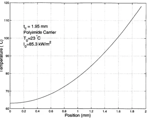
sur-face flux. . . . . 44 2-10 Temperature profile for low conductivity carrier. . . . . 46 2-11 Temperature profile for high conductivity carrier. . . . . 46
3-1 Section of an industry standard carrier tray for 10 mm QFP devices. 54 3-2 Section of strip carrier. Carrier on right is original metal lead frame,
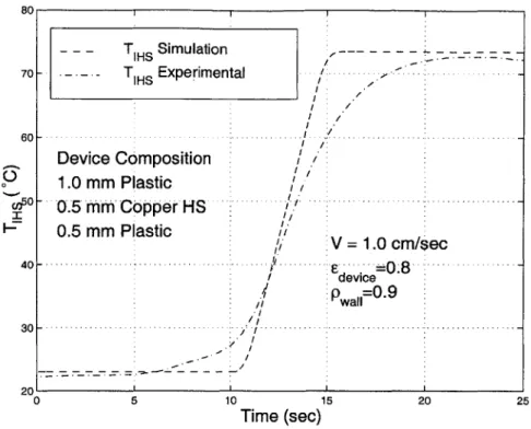
carrier on left has been overmolded. Width of frame is 5.84 cm. . . . 55 3-3 IR heating chamber assembly. . . . . 57 3-4 Photograph of assembled IR heating system. . . . . 58 3-5 Temperature profile in 10 mm QFP device at exit of heating chamber. 61 3-6 Temperature profile through a plastic carrier after exiting heater section. 62 3-7 Temperature profile along strip carrier metal frame for Io = 65.7
3-8 Resistance model for encapsulated strip device. The hatched area
rep-resents the region where conductivity is assume to be infinite. .... 66
3-9 Experimental data for testing lateral heating uniformity with high re-flectivity chamber walls. Data is for 10 mm QFP device mounted on leading row of plastic carrier. Temperature measured on integral heat spreader... ... ... 68
3-10 Experimental data for testing lateral heating uniformity with low re-flectivity chamber walls. Data is for 10 mm QFP device mounted on leading row of plastic carrier. Temperature measure on integral heat spreader. . . . . 69
3-11 Experimental and simulation data for 10 mm QFP on carrier centerline. 70 3-12 Temperature profile for high conductivity carrier. . . . . 71
3-13 Temperature profile for heating of strip carrier. . . . . 72
3-14 Settling time for device in center of carrier compared to surrounding m etal fram e. . . . . 72
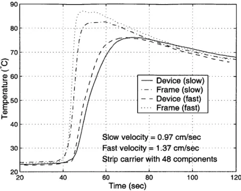
3-15 Heating of strip carrier at two different carrier velocities. . . . . 73
3-16 Temperature profile for heating of 10 mm QFP devices. . . . . 75
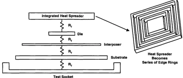
4-1 Cross-section of typical high power density device. Some components may not be present in some devices. . . . . 78
4-2 Intel P858ACY TTV . . . . 80
4-3 Intel Pinetop TTV . . . . 81
4-4 Baseline Intel power profile . . . . 82
4-5 Baseline transient model of a typical device under test. . . . . 83
4-6 Experimental and simulation data for a P858ACY TTV subject to a 93.2 W Intel power profile. . . . . 86
4-7 Experimental and simulation data for a P858ACY TTV subject to a 70 W step power profile. . . . . 87
4-8 Experimental and simulation data for a Pinetop TTV subject to a 23.3 W Intel power profile. . . . . 89
4-9 Physical model of system updated to include lateral conduction in the integrated heat spreader. . . . . 90
4-10 Diagram for calculation of conduction resistance between ring segments on the IHS. ... ... 91
4-11 Experimental and simulation data for a Pinetop TTV device subject to the Intel test sequence. ... ... 92 4-12 Expanded view of the data in Fig. 4-11 . . . . 92 5-1 Single and stacked nozzle modules. . . . . 95 5-2 Side view and cross sectional view of assembled laser/convection
sys-tem. Manifold system and base support structure not shown. . . . . . 100 5-3 Schematic diagram of control and data acquisition system for laser/convection prototype system . . . . 102
6-1 Test apparatus for measuring convective transfer coefficients on a sim-ulated electronic device. . . . . 112 6-2 Schematic drawing of nozzle test system. . . . . 112 6-3 Detailed view of the heater section of the nozzle test assembly. Views
are shown with and without a device holder. . . . . 114 6-4 Correlation and experimental data for Reynolds number versus the
convection coefficient K, for the nozzle test rig. Error bars show the experimental measurement errors in Red and Tc. Data is for a flat face conduction plate configuration (no side edges exposed) with no device holder present. . . . . 116 6-5 Measured values of h for increasing power dissipation levels at Red =
14500. Correlation value is T, = 1400 W/m2K. Flat face configuration with no device holder present. . . . . 117 6-6 Correlation and experimental hc values for multiple H/D ratios.
Ex-perimental data is for no exposed side edges and no holder present. . 118 6-7 Average side edge convective heat transfer coefficients for various
ex-posed side face heights. . . . . 119 6-8 Detailed view of simulated die holder for convection experiments. The
recessed grooves mount on the four corners of the copper block. . . . 121
6-9 Effective heat transfer coefficient for various side edge exposure heights with no device holder and with PEEK device holder present. . . . . . 122 6-10 Percent decrease in he when a PEEK device holder is added for a
specified exposed edge height. . . . . 123 6-11 Measured he for various holder materials and flat plate configuration
with no holder. . . . . 124 6-12 Noise level at a position 1 cm from the nozzle assembly. . . . . 124
7-1 Manifold pressure versus h, for the prototype system. . . . . 130 7-2 Volumetric flow rate under standard conditions versus manifold pressure. 130
7-3 Die temperature for Pinetop TTV subject to a 23.3 W Intel test sequence. 131 7-4 Single channel data for Pinetop TTV subject to 23.3 W Intel test
sequence. ... ... 132 7-5 Temperature response of Pinetop TTV subject to a 14 W Intel power
sequence with no forced convection. . . . . 133 7-6 Temperature response of Pinetop TTV to scaled Intel test sequences
with constant manifold pressure. . . . . 134
7-7 Temperature response of Pinetop TTV for a 23 W Intel test sequence
at multiple manifold pressures. . . . . 135 7-8 Die temperature for a P858ACY TTV subject to a 46.7 W Intel test
sequence. ... ... 136 7-9 Uncontrolled and controlled temperature response of a Pinetop TTV
to a 46.7 W Intel test sequence. . . . . 137 7-10 Controlled temperature response of a Pinetop TTV to a 23.3 W Intel
test sequence. ... ... 138 7-11 Control power sequence for Pinetop die temperature response shown
in Fig. 7-10. . . . 139 7-12 Controlled die temperature response to 23.3 W Intel test sequence at
multiple manifold pressures. . . . . 140
7-13 Uncontrolled and controlled temperature response of a Pinetop TTV
to a 46.7 W Intel test sequence. . . . . 141 7-14 Controlled temperature response of a P858ACY TTV to a 46.7 W Intel
test sequence. ... ... 142
7-15 Control power sequence for P858ACY TTV die temperature response shown in Fig. 7-14. . . . . 143 7-16 Decomposition of Intel test sequence. . . . . 145
7-17 Uncontrolled and controlled temperature profile of a Pinetop TTV to
the 5 second average power profile with a peak power at 50.2 W. . . . 146
7-18 Experimental limits of temperature control for 5 second power average
with Pinetop TTV. . . . . 146
7-19 Peak control power versus peak die power for 5 second average power
7-20 Temperature variation across the die for controlled and uncontrolled 5 second average test sequences. . . . . 147 7-21 Die power and laser power as a function of time for temperature control
of a Pinetop TTV with a 5 second average power sequence. . . . . 148 7-22 Uncontrolled and controlled temperature profile of a P858ACY TTV
to the 5 second average power profile with a peak power at 53.2 W. . 149 7-23 Experimental limits of temperature control for 5 second power average
with P858ACY TTV. . . . 150 7-24 Peak control power versus peak die power for 5 second average power
sequence on a P858ACY TTV. . . . . 150 7-25 P858ACY TTV temperature variation across the die for controlled and
uncontrolled 5 second average test sequences. . . . . 151 7-26 Die power and laser power as a function of time for temperature control
of a P858ACY TTV with a 5 second average power sequence. . . . . 151 7-27 Uncontrolled and controlled temperature profile of a Pinetop TTV to
the 1 second average power profile with a peak power at 36.0 W. . . . 152 7-28 Experimental limits of temperature control for the 1 second power
average with Pinetop TTV. . . . . 153 7-29 Peak control power versus peak die power for the 1 second average
power sequence on a Pinetop TTV. . . . . 153 7-30 Die power and laser power as a function of time for temperature control
of a Pinetop TTV with a 1 second average power sequence. . . . . 154 7-31 Uncontrolled and controlled temperature profile of a P858ACY TTV
to the 1 second average power profile with a peak power at 48.0 W. . 155 7-32 Experimental limits of temperature control for the 1 second power
average with a P858ACY TTV. . . . . 156 7-33 Peak control power versus peak die power for the 1 second average
power sequence on a P858ACY TTV. . . . . 157 7-34 Die power and laser power as a function of time for temperature control
of a P858ACY TTV with a 1 second average power sequence. . . . . 158 7-35 Detailed view of remainder power sequence. . . . . 159 7-36 Controlled and uncontrolled temperature response of Pinetop TTV die
to the remainder power sequence. . . . . 160 7-37 Controlled and uncontrolled temperature response of P858ACY TTV
8-1 Comparison models for proof of isothermal die assumption. . . . . 166 8-2 Magnitude of temperature fluctuation for distributed generation and
surface flux on adiabatic die structure. . . . . 168 8-3 Phase shift of IHS side temperature for surface flux case. . . . . 169
8-4 Die cut off frequency for the Intel P858ACY TTV at various temper-ature tolerance levels and power levels. . . . . 171 8-5 Die cut off frequency for the Intel Pine-Top TTV at various
tempera-ture tolerance levels and power levels. . . . . 172 8-6 Physical model for die power to control power ratio calculation. . . . 173 8-7 Control power to die power ratio versus exponential settling times of
the die power for the Intel Pinetop TTV. . . . . 175 8-8 Die power and control power for dual mass model based on -r = 0.025
sec.. . . . ... 176 8-9 Schematic diagram of simplified device for transient analysis. Q, is the
magnitude of the control input and a is the phase shift of the control input. Qd is the magnitude of the die power profile. . . . . 179 8-10 Schematic drawing of decomposition for solution to transient
temper-ature profile in integrated heat spreader. . . . . 180 8-11 Graphical solution for phase shift and magnitude of control power profile. 183 8-12 Temperature response of IHS to a 10 Hz die power profile with Qd =
10 W/cm2. For this system, h, = 1200 W/cm2 and the IHS is 1.8 mm
thick. . . . . 184 8-13 Temperature response of IHS to a 10 Hz die power profile with Qd =
10 W/cm2 and a control power profile imposed on the front face.. . 185
8-14 Solution for phase shift and control magnitude for ideal temperature control of die. . . . . 187 8-15 IHS temperature profile for ideal control of die temperatures. . . . . . 188 8-16 Magnitude and phase shift of control profile to maintain die
tempera-ture within 4 K for a 10 Hz die power profile with Qd = 10 W/cm2. . 191 8-17 Temperature profile in die and IHS for 10 Hz die power profile with
magnitude of 10 W/cm2 with AT = 4 K. . . . . 192
8-18 Incremental segment break-down for finite difference confirmation model. 193 8-19 Calculated die temperature using finite difference model to confirm
analytic solution for control input . . . . . 195 8-20 Control input and die temperature for square wave die power profile. 196
8-21 Control input and die temperature for triangular wave die power profile. 197
8-22 Control limits for specified die power profile. . . . . 198
8-23 Control limits for specified die power profile. . . . . 199
8-24 Limits of control for multiple values of the convective heat transfer coefficient h.. . . .. . . . 200
8-25 Effect of die to IHS thermal resistance on control limits. . . . . 201
8-26 Effect of IHS thickness on control limits. . . . . 201
8-27 Effect of die thickness on control limits. . . . . 202
8-28 Solution for temperature profile propagation time for integrated heat spreader. . . . . 203
8-29 Minimum changed in die temperature for under ideal feedback control conditions. . . . . 204
8-30 Device to device variation in temperature response for common power sequence. . . . . 206
8-31 Segmentation of IHS for lateral conduction calculations . . . . 208
8-32 Transient fin temperature profile for Pinetop TTV . . . . 209
8-33 Lateral conduction into Pinetop TTV IHS for multiple frequencies with hc = 1200 W/m2K.
Q
represents the total energy loss due to transient conduction into the edges of the IHS. AT represents the magnitude of the fluctuation of the temperature of the IHS directly over the die structure. . ... ... ... ... ... . . 2108-34 Lateral conduction (Q) into Pinetop TTV IHS for a range of he values for a 10 Hz base temperature fluctuation of AT. .. . . . . 211
8-35 Transient fin temperature profile for Pinetop TTV with AT = 4 K at 40 Hz. Top plot represents temperature profile at base, middle, and tip of fin. Bottom plot represents maximum temperature defect along the length of the fin. . . . . 212
8-36 Steady state temperature profile for Pinetop TTV. . . . . 214
8-37 IHS temperature as a function of he for 20 W control power input. . . 214
8-38 Steady state temperature profile for P858ACY TTV. . . . . 215
8-39 IHS temperature distribution for small illumination spot size on the Pinetop TTV . . . . 216
8-40 IHS temperature profile for Pinetop TTV with 20 W die input. . ... 217
8-42 IHS temperature profile for Pinetop TTV with 20 W die and 20 W control input. ... ... 219 8-43 IHS temperature profile for P858ACY TTV with 20 W die and 20 W
control input. ... ... ... 220 9-1 Control limit plot for Intel Pinetop TTV and P858ACY TTV for 46.7
W peak power and AT = 2'C. . . . 224 9-2 Comparison of temperature control limits of Pinetop TTV and P858ACY
TTV for a 46.7 W Intel test sequence. . . . . 226 9-3 Results of a discrete Fourier transform on each of the decomposed
power profiles. . . . 228 9-4 Experimental data for P858ACY TTV and Pinetop TTV for
compar-ison with control limit theory. . . . 229 9-5 Experimental data versus control limit theory for 1 second and 5 second
power profile sequences. . . . . 230 9-6 P858ACY TTV uncontrolled temperature response to scaled remnant
power profiles. . . . . 231 9-7 Uncontrolled temperature limits for P858ACY to scaled remnant power
Nomenclature
Symbol Description
a, b, c geometric factors in conduction resistance calculation [im]
at thermal diffusivity [M]
A, A1, A2 integration constant
Acu cross sectional area of heated copper block [m 2
]
Adevice total device surface area exposed to radiation [iM2
]
A!ace top surface area exposed to convection [iM2
]
A, apparent contact area between device and carrier [m 2]
Aped pedestal cross sectional area [iM2
]
Aside side surface area exposed to convection [iM 2
] b integrated heat spreader thickness [m]
b RTD calibration intercept
B, B1, B2 integration constant
Bi Biot number - Eqn. 8.2
BiR modified Biot number - Eqn. 8.3 specific heat
[g]
C integration constant
C1, C2 Planck's constants
Cn constant in infinite sum
D internal nozzle diameter [im] D, D1 integration constants
EbA black body spectral distribution [W]
f
nozzle geometry factor - Eqn. 6.2 F1 integration constantFdA_1 view factor from small area dA to area 1
Fo Fourier number
hc average convective transfer coefficient [W]
hface convective transfer coefficient on top surface of target [n2]
hside convective transfer coefficient on side surface of target [W]
H nozzle to target plate spacing [m] i imaginary number - VI T
10 incident surface radiation intensity
[2]
Ia absorbed radiation intensity
[]
Ic collimated radiation intensity[W]
Id diffuse radiation intensity [y]
k thermal conductivity [A]
kair thermal conductivity of air
[ ]
kPEEK thermal conductivity of PEEK pedestal
[W]
K thermal mass of die [y]
L interstitial gap length [im] L frequency coefficient - Eqn. 8.25
Lt orthogonal nozzle spacing [im]
LTC thermocouple spacing in PEEK pedestal [m]
m RTD calibration slope
M energy transfer correction factor - Eqn. 8.51
M1 integration constant
MC thermal mass of carrier
[y]
Md thermal mass of device [j]
n index of refraction
N1 integration constant
Nu Nusselt number - Eqn. 6.1
P fin perimeter [im]
P1 integration constant
PTTV power applied to thermal test vehicle [W]
Pr Prandtl number
P.P. pumping power - Eqn. 6.13
PS1, PS2 integration constants
QcU power conducted through copper block [W]
Qpedestal power conducted through PEEK pedestal [W]
Qsq square wave die power [W]
Qt,.
triangular wave die power [W]Qd die power density
[]
QC
control power density[W]
r, control power illumination radius [m]
r2 outer IHS radius [im]
Ro TTV die resistance at 00C [Q]
R, integration constant
Rf calibrated TTV die resistance [Q]
Rm measured TTV die resistance [Q]
Rt thermal contact resistance [Km]
ReD Reynold's Number
s Laplace operator
s material depth [m]
t time [sec]
tc carrier thickness [m]
tss steady state settling time [sec]
TO initial temperature [K]
Tair air temperature [K]
TBF IHS die side temperature [K] TcU copper surface temperature [K]
TLC pedestal lower thermocouple temperature [K]
TUT pedestal upper thermocouple temperature [K]
U1 integration constant
V1 integration constant
Greek Symbols
a phase shift [radians]
a shaped fin geometry factor
an infinite series constant phase shift [radians]
6 error term
C emissivity
K absorption coefficient [cm-1]
A integration constant
A wavelength [Am]
An infinite series constant
E
temperature defect [K]p surface reflectivity
a rms surface roughness [m]
Chapter 1
Introduction
In the electronic component manufacturing industry, most components are subjected to a full functional test before they are sold. Depending on the type of components, these functional tests may be performed at room temperature, at cold temperature, or at high temperature (-50*C to 160C) depending on the type of component and intended market' [1, 2]. The thermal management of these components during testing forms two basic issues that need to be addressed. The first issue is the heating or cooling of devices to the desired temperature prior to being tested, and the second issue concerns temperature control during the actual functional test.
Thermal conditioning of devices prior to testing is becoming more important as test equipment technology enables increased parallel testing and reduces required test times. The actual time required for electrical test of some components can be less than 1 second, while traditional air convection soak chambers may take 20 to 60 minutes [2] to bring devices up to the test temperature. The time required for testing is only a very small fraction of the total test cycle time. This is especially true in the case of parallel testing where up to 64 components can be tested at a time. In order to reduce the total test cycle time and make the testing process more efficient, a new method is required to rapidly bring multiple components to test temperature. This thesis will describe a new method that utilizes infrared radiation to heat components. Target ramp rates of ±6oC/sec to t60'C/sec have been set, but as will be shown, the main limitation in device heating is due to the physical design of the package. The problem then becomes a case of calculating the maximum heating rate based on
1Under the hood automotive components and military components tend to be tested at the temperature extremes.
component packaging and then designing the system around the upper limit.
Temperature control of devices during the functional test is primarily an issue for high power microprocessor devices. With increasing levels of integration, reduced component size, and increasing clock speeds, the total thermal power dissipated and power density of microprocessors is rapidly increasing. During the testing process, device manufacturers specify a minimum device temperature. The higher the tem-perature deviation over this temtem-perature, the higher the risk of classifying a device in the wrong category2. With increasing power dissipation levels, it is becoming more difficult to keep the temperature of the device under test (DUT) constant using only passive methods. Some form of active temperature control is required for managing the thermal drift during testing. Typical functional tests on a microprocessor make last 1-2 minutes with the power cycling from almost zero power to full power on a very rapid basis.
There are two primary methods that have been proposed for thermal control of an active device during testing. One method described in a UNISYS patent [3] utilizes a large thermal mass with embedded heaters and cooling channels in direct contact with the device. The temperature of the thermal mass can be controlled very tightly, thereby controlling the temperature of the device under test. This method requires physical contact between the device and control mass, and the thermal contact re-sistance can vary significantly due to low contact pressures and variations in surface conditions. This variation in contact resistance makes reliable thermal control diffi-cult. The contact resistance variation can be significantly reduced through use of a thermal interface material (liquid or soft solid interface), but electronic manufacturers are very resistant to this idea because it will required an additional step to clean the devices after testing3 and will increase the cost and time of the testing process.
An alternate approach utilizes radiation and convective cooling to control the temperature of the device under test. The convection system is capable of handling the full thermal load produced at 100% device power, but due to capacitance and flow resistance, the convective cooling cannot be controlled at a sufficiently rapid rate to control the temperature of the device by itself. Instead, the convective cooling is held constant, and constant die temperature will be obtained through use of a controllable
2For example, classifying a 1 GHz microprocessor as a 950 MHz device. Increasing device
tem-peratures can reduce signal propagation speed within a device.
3Solid thermal interfaces generally have liquid silicon or some other liquid imbedded in them and
radiation source. This system requires no contact between the device and control system so variable thermal contact resistance is no longer a problem. A prototype system has been developed that utilizes high performance impingement cooling and laser heating to control the temperature of a device. The system will be described in this thesis, as well as experimental test results from the prototype system.
The mathematical theory for the temperature control system will be developed. Critical parameters will be identified and theory will show the impact of the test sequence design on the fundamental limits of temperature control for a device under test conditions.
Chapter 2
Infrared Heating Theory
Three possible methods are available for rapidly heating and cooling multiple com-ponents: convection, conduction, and radiation. Convection is the most common method currently used in industry, but there are significant limits to this technology. In order to increase the heating rate of a group of devices, either the air tempera-ture needs to be increased or the convective transfer coefficient needs to be increased. Increasing the air temperature increases the risk of overheating devices, and it can be fairly complicated to obtain small zones of high temperature convective heating due to baffling requirements. Increasing air temperatures also results in lower system efficiency as more energy is wasted in air loss and external convection/conduction losses. Increasing air velocities can cause loose mounted devices to be blown out of the carrier, which limits this approach to increasing the convective heat transfer co-efficient. Also high air velocities on a large scale can cause significant noise problems that would required additional insulation on the test handler.
Conductive heating is difficult to implement for multiple devices. Manufactur-ers do not want to use interface materials that leave a residue or require a secondary cleaning process, so all thermal interfaces are dry contact. Without high contact pres-sures, which have the potential to damage devices, the thermal interface resistance between a heater and device can vary significantly. This means each device tempera-ture must be measured and a form of feedback control must be implemented to bring components to a uniform temperature. This is possible with single device testing and can even be implemented for several devices at once, but with large parallel testing', this can be very difficult and expensive. Just trying to obtain an even pressure
tween multiple devices and a heating chuck can be difficult, let alone measuring and controlling the temperature of each device. Granted, the heating chuck can be kept at the target temperature, but because the temperature difference between a compo-nent and the chuck decays expocompo-nentially, this doesn't fulfill the requirement for rapid heating.
Radiant heating provides one of the best options for rapid heating of multiple components, but a number of factors must be considered. The device packaging and material will dictate the usable wavelengths. Uniform heating of multiple components requires proper selection of the radiant source and heating chamber in order to pro-duce a uniform radiation field. The final temperature of the device will depending on the heating of the component and the heating of the carrier, and an accurate device model is required to avoid overheating of the device surface. The proposed system for heating of multiple components is composed of an off-the-shelf IR heater with shields to block the end effect of the IR bulb and a high reflectivity heating chamber to pro-duce a uniform radiation field. To model the heating of devices, a basic background in radiation is required.
2.1
Radiant Heating
The heating of a device using infrared radiation is a function of the radiation field and the radiation properties of the device. Assuming a uniform radiation field intensity I, the energy reflected from the surface is simply given by I, = p-Io where p is the surface reflectivity [4]. Unfortunately, p is a function of the incident wavelength A, surface conditions, material type, material temperature and incident angle of radiation. The energy that is not reflected is either absorbed by the material or transmitted through the material. The radiation absorbed over a material thickness s is given by
Ia = (1 - p) Io (1 - e-Ns) (2.1) where K is the absorption coefficient of the material and is generally specified in units of cm- 1. Again, r is a function of wavelength, material and temperature.
For infrared heating of devices, it is desirable to have a low surface reflectivity to increase the effective heating rate. Also, all the energy should be absorbed in the device encapsulant with little or no radiant energy propagating through to the active die region of the device. Radiation that propagates through to the active die has the potential to interact with active components to create photocurrents that can cause
Table 2.1: Reflectivity and absorption coefficients for common device materials. Material Short Infrared Short Infrared Long Infrared
Type 800 nm 1.06 pm 10.6 pm Silicon [5] p ~ .3 p p ~ .2 - .7 r ~ 104 cm-1 r ~ 1.5 cm- 1 r-~ 1.5 cm-1 Al2O3' [5] P ~ .8 - .9 P ~ .9 - 1 P .1 - .15 r ~ .009 cm-1 K ~s .009 cm- 1 r > 100 cm-1 Si0 2c [5] p ~ .8 - .9 P 9 - .9 5 p ~ .1-.2 K ~ .004 cm-1 ~ .004 cm-1 K > 100 cm 1 Polyimide p ~ .2 p ~ .2 p ~ 1 Plasticsd [6] r, ~,., 10 - 20cm-1 i ~- 10 - 20 cm- K - 300 - 700 cm-1 Ni coated p ~~ .6 p ~1_ .8 p ~ .95 Cue [7] K ~ 105 cm-1 K ~ 105 cm-1 r ~ 10K 5 cm-1
aHighly dependent on doping type and quantitiy. bCrystalline.
'Fused.
dRepresentative values only. Actual values strong function of specific plastic composition.
ep values are a strong function of surface conditions.
erroneous results in the testing process, or if the radiation intensity is sufficiently high, the potential exists to actually damage active components on the device. The wavelengths that must be considered for IR heating extend from the near ultraviolet
A ~ 300 nm to the far infrared A ~ 15 pm. There are four common types of packaging
material that must be considered over these wavelengths: metals, plastics, ceramics and silicon. Selection of a radiation source now becomes a matter of selecting an operating wavelength region over which the device has low reflectivity with a high absorption coefficient. Both requirements cannot always be fulfilled simultaneously, so selection of a radiation source becomes a compromise between low reflectivity and high absorptivity. Table 2.1 presents representative reflectivity and absorption data for some common packaging materials at three different wavelengths. For the majority of materials, with material thicknesses of 1 mm or greater, the materials are effectively opaque at all wavelengths, or in other words, all of the radiation is effectively absorbed and very little is transmitted through the layer. For this reason, all devices will be treated as non-transparent for modeling purposes.
The characteristics of the radiation incident on the surface of a device are depen-dent on the operating temperature and emissive properties of the IR source. The general distribution of energy for a black body can be calculated from
EbA = (2.2)
(n - A-T)5 x n -T
where C1 = 3.7914 x 10⁻¹⁶ WM2, C2 = 14388 pim K, and n is the refractive index and is taken equal to 1 for gases. The total emissive power over a wavelength region can be calulated by integrating eqn. 2.2 over the specified wavelength. This integral is tabulated in most radiation heat transfer text books [4, 8]. This can be useful for calculating how much of the incident energy is in the visible, IR, and ultraviolet regions and for calculating heat transfer rates.
The system developed for heating of multiple components consists of a single quartz-tungsten bulb mounted in a parabolic reflector assembly. Multiple devices on a carrier are passed under the output of the bulb-reflector assembly. Figure 2-1 shows a typical cross section of a proposed heating system. Two main challenges arise in heating components using this method, both of which involve heating components in different positions on the carrier to the same temperature. The first problem is to hold a uniform temperature for all devices along a line perpendicular to the direction of carrier motion. This requirement is not generally a problem if there are only 1-2 components across the carrier, but, for situations with 3 or more components, it is harder to keep the edge components at the same temperature as the central components. This problem can be addressed by suitable selection of the radiant heater, surface properties, and geometry of the thermal chamber, so that the radiation field is uniform across the device carrier.
The second challenge in producing uniform device temperatures is in heating a device on the leading edge of the carrier to the same target temperature as a device on the trailing edge of the carrier. This problem is solely a function of the carrier type. For low conductivity carriers with high thermal resistance between the device and carrier, such as plastic trays with loose mounted devices or polymer-sheet strip carriers, conduction along the carrier does not have to be considered, and leading-edge and trailing-leading-edge devices are easily heated to the same temperature without additional thermal control. For high conductivity carriers, such as lead-frame strip carriers and metal transport trays, conduction along the carrier can cause trailing-edge devices to be heated to a higher temperature than leading-trailing-edge devices. Under
T
H
Quartz Tunsten Bulb nParabolicReflector Collimated Radiation Diffuse Imaginary Radiation Black SurfaceI I
I
Components I, l El El E 4-Direction of MotionFigure 2-1: Cross section view of proposed IR chamber.
final steady state conditions, the temperatures of trailing and leading-edge devices will be the same, but the transient effect of carrier conduction must be analyzed to prevent overheating of components and to minimize the settling time after exiting the IR heating system.
2.2
IR Heating Model
Three parts are involved in modeling the heating of devices using an IR source. One part is associated with the heating of the actual devices, another with the heating of the device carrier, and the third is associated with the coupling between the carrier and the devices. The main objectives of the modeling are to determine the feasibility of obtaining uniform device temperatures and to determine the parameters that are critical to the final design.
2.2.1
Component Heating
The radiant heat transfer from the IR source to an individual device can be calculated using traditional resistance network methods, but the method must be modified in order to account for the effect of collimating reflectors on the radiation field. Figure 2-1 shows a cross-sectional view of a proposed heating chamber and Fig. 2-2 presents an isometric view of the heater and carrier. To keep the size of the heating system to a minimum, the heater is assumed to be the same width as the carrier. Rather than analyzing the IR source and parabolic reflector, the emitted radiation from the IR bulb is separated into a diffuse and collimated component. The IR bulb and reflector assembly can then be treated as an imaginary surface with two specified radiant fluxes, one collimated and the other diffuse. The ratio of collimated to diffuse radiation will depend on the design and reflectivity of the parabolic mirror and the placement of the bulb. The radiant intensity from the bulb can be assumed uniform around its circumference. Then, if a parabolic reflector with the bulb set deep inside the reflector is used, the majority of the emitted radiation will intersect with the reflector and will be reflected as collimated radiation. Conversely, for a very shallow reflector surface, most of the radiation will be diffuse with only a small fraction of the total emission intersecting the reflector surface and becoming collimated. The position of the bulb and reflector are generally fixed for a given design, and the ratio of collimated to diffuse radiation cannot easily be changed. Modeling will be used to
Figure 2-2: Isometric view of IR chamber.
evaluate the effect of various collimated/diffuse ratios, but a good starting baseline is to assume half is diffuse and half is collimated. The radiation emitted from the bulb is also assumed to be uniform over the entire width of the heating chamber2
View factors between a device and all surrounding surfaces can be easily calculated for parallel surfaces using
1 [ A 1 B B A
FdA_1 d- = 2,7r -[ vl - A2 A2 tan~1+A1+ A2 2 + V1 +B2 tan V1 + B2 (3 where A = a/c, B = b/c, and a and b are the dimensions of the wall, and c is the distance between the small area and one corner of the wall [4]. For perpendicular surfaces, the view factor can be calculated from
FdA1 = -[tan1tan 1
X2tYnl
(2.4)27r Y Xfy VX2 -y 2
where X = a/b, Y = c/b, a is the height of the wall, b is the width, and c is the horizontal distance between the lower corner of the wall and the center of the small area dA [4].
These view factor calculations are valid for radiation transfer between a small surface and a parallel or perpendicular surface with one corner in line with the center
2
The end effects of the bulb are neglected.
Parabolic Mirror
(cut away view)
Heating Chamber
Quartz-Tungsten
Bulb Device Carrier with Direction of
Components
Al
Figure 2-3: Areas for view factor calculations.
of the small area. Based on the position of the device, the surrounding surfaces were broken up into rectangular segments such that one corner of each segment was in line with the center of the small area dA as shown in Fig. 2-3 for two of the four side walls. The device was broken into a number of small sections whose area is much smaller than any single wall section and the total view factors were found by discrete integration over the entire component surface to the surrounding segmented surfaces. With all view factors known, the total energy transfer from collimated and diffuse radiation can be calculated. Heat transfer from the collimated radiation is simply given by
QC
= aAdeviceIc (2.5)where Adevice is the component surface area exposed to the radiation field, a is the device absorptivity, and I, is the collimated radiation intensity. Heat transfer to the device from diffuse bulb radiation can be combined with radiant exchange between the device and the chamber walls, and the total heat flux can be found using a traditional resistance network. In the resistance model, the imaginary surface in Fig. 2-1 is treated as a black surface at the same temperature as the component, but with a specified radiant emissive power (i.e. there is no loss from the device to the imaginary surface, but the imaginary surface has a specified flux). This assumption of a black surface neglects the higher intensity directly under the bulb, but this effect
3A A2
A4
is reduced due to an imperfect parabolic reflector surface and the bulb is not a true line source at the focus of the parabola3.
The devices are assumed to be flat with no interaction between adjacent devices and no exposed edges. For any given position within the heating chamber, all view factors can be calculated and the total heat transfer to a device can be found as the sum of the collimated heat transfer and the diffuse heat transfer. Each chamber wall is assumed to be a diffuse isothermal surface with specified emissivity and reflectivity. The temperature of each wall can be set independently. The collimated radiation is assumed to have no secondary effects on energy transfer to the devices4. By breaking the progress of a device through the heater as a series of small discrete steps, the heat transfer at each position in the heating chamber can be calculated, and the device temperature may be found from
dT
MD- = Qc + Qd (2.6)
dt
where MD = mdCp is the thermal mass of a device,
Qc
is the heat transfer from the collimated radiation, Qd is the heat transfer from the diffuse radiation and interaction with chamber walls at each position, m is the component mass, c, is the specific heat, t is the time elapsed since entering the chamber, and T is the average temperature of the component. Entrance and exit effects are treated by assuming partial shielding of each device. The diffuse radiation transfer Qd is a function of the component temperature as this term contains radiant transfer between the device and the walls. The component temperature used in this calculation is the device temperature from the previous step.A computer simulation was constructed using this method to analyze the effects of various heater geometries and other physical parameters on the temperatures of components across a carrier. Of main interest is a comparison of the temperature rise of a component on the edge of a carrier to that of a component in the middle of the carrier. The standard component selected for the simulation is a plastic encapsulated 10 mm QFP5 device. This device consists of a silicon die mounted on a 0.5 mm thick integrated copper heat spreader with 1 mm of plastic encapsulant on the top surface
3Higher intensity directly under the bulb will affect final device temperature, but will have a
limited effect on temperature uniformity across the carrier.
4Primary and secondary reflections of the collimated radiation are neglected. The collimated
radiation is assumed to have no interaction with the chamber walls.
5
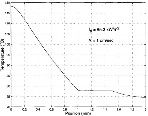
80 I -~ 70 60 CU C.50 E CD I-40 0 20L L 0 1 2 3 4 5 6 Time (sec)
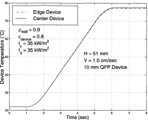
Figure 2-4: Average device temperature for a 10 mm QFP package with high reflec-tivity chamber walls.
of the device and 0.5 mm of plastic encapsulant on the bottom surface. The radiation intensity for the collimated radiation and diffuse radiation was set at a representative output of 70 kW/m 2 with a constant carrier velocity of 1.0 cm/sec.
While the absolute values of the radiation intensity and carrier velocity will affect the final temperature of the device, of interest is their effect on the temperature difference of devices across a carrier. This means one of the parameters of interest is the ratio of the collimated to diffuse radiation intensity. Other parameters that can affect the temperature difference between components is the height of the heating chamber6, the wall side reflectivities and temperatures, and the collimated/diffuse intensity ratio. All devices are assumed to be at an initial uniform temperature with uniform radiation properties. Weed and Kirkpatrick [9] have estimated the emissivity of a plastic encapsulated QFP package as 6 ~ 0.9. The QFP package is assumed to
be a grey body with e = a.
6
While the height of the chamber can be modified, the depth of the chamber in direction of motion and width of the heater are assumed fixed.
-- -Edge Device Center Device Pwail 0.9 - device -| 5kW/m C d2 135 kW/rn d H=51 mm V = 1.0 cm/sec 10 mm QFP Device 80 30
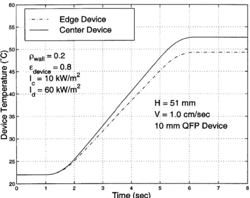
65- - -- Edge Device Center Device 60 - - - - --0 55 -. -.Pw a l- = 0- .2 -- --- --- - - -.---.- . .---- . --=0.8: Edevice = -1- ....- I -4:35- kW / m -... 2 V (D' I =35 kW/m2 E H = 51 m m V1 .0 cm/sec 10 mm QFP Device 20 Time (sec)
Figure 2-5: Average device temperature for a 10 mm QFP package with low reflec-tivity chamber walls.
2.2.2
Device Modeling Results
Figure 2-4 shows the average temperature response of two devices, one on the edge of the carrier, one at the center. This figure is for the case with wall reflectivity of
0.8, wall temperatures of 27'C on the two side walls and one end wall, and a wall
temperature of 770C on the remaining wall. The chamber dimensions are 150 mm
wide by 41 mm deep by 51 mm high. As can be seen, the edge and center devices are at almost identical temperatures. Figure 2-5 presents data for the same parameter values, but with the wall reflectivity changed from 0.8 to 0.2. Two main effects can be observed from reducing the wall reflectivity while keeping all other parameters the same. The final component temperature is reduced and there is now about 3*C difference between the edge device and the center device. This shows that from a pure efficiency perspective, high reflectivity walls are preferred to increase the fraction of radiant power that is transferred to the components and to keep the chamber walls at a lower temperature.
70 60 0-50 E CD C-0 0 20 L-0 3 4 5 6 Time (sec)
Figure 2-6: Average device temperature for a 10 mm QFP package with a wall height and low wall reflectivity.
5 mm side
reduced to 5 mm with low reflectivity. As is expected, when the side walls are almost eliminated, reflection effects no longer matter and there is very low absorption by the walls, so the device temperatures are more uniform and the final temperature is close to the case with high reflectivity walls. Figure 2-7 presents the results for a high ratio of diffuse/collimated radiation, and Fig. 2-8 presents the results for a low diffuse/collimated ratio. Both sets of results are for low reflectivity walls (p = 0.2) with a wall height of 51 mm. These results demonstrate that under the assumption that end effects of the IR bulb can be neglected and that output is uniform across the width of the chamber, rapid uniform heating of multiple component is possible with the best results obtained for high reflectivity walls with small distances between the devices heater surfaces. The physical implementation of the assumption to neglect bulb end effects will be discussed in the apparatus section.
Equation 2.6 illustrates another factor that must be considered in the analysis of component heating using IR radiation. Very high heat fluxes are possible at the surface of the device, so conduction through the device must be considered. While eqn. 2.6 will provide information about the average temperature of a component as
M) --- Edge Device Center Device Pwaii = 0.2 -. 08 device I = 35 kW/m: C I = 35 kW/m V 1.0 cm/sec 10 mm QFP Device 30 1
Center Device ( - v = 0 .8 I =10 kW/n I=60 kW/M E CD H= 51 mm 03 - V= 1.0 cm/sec 10 mm QFP Device 0 3 0 -. . .-..-..-.-..-..-.-..-..-.-.. -.. -. -.. -20 0) 1 2 3 4 5 6 7 8 Time (sec)
Figure 2-7: Average device temperature for a 10 mm QFP package with a large diffuse to collimated radiation intensity ratio.
E g I I
- --- - Edge Device
70 0 60 0-50 E I-40 a)0 0 Figure 2-8: u I 1 1 -- - Edge Device Center Device Pwal = 0.2 device 1 =:60 kW/m d H=51mm V = 1.0 cm/sec ... 10 mm QFP Device. -0- -- -- 1 2 ---. 3 4 --- -- -- - -- . 0 1 2 3 4 5 6 7 8 Time (sec)
Average device temperature for a 10 mm QFP package with a small diffuse to collimated radiation intensity ratio.