HAL Id: cea-01217063
https://hal-cea.archives-ouvertes.fr/cea-01217063
Submitted on 18 Oct 2015
HAL is a multi-disciplinary open access
archive for the deposit and dissemination of
sci-entific research documents, whether they are
pub-lished or not. The documents may come from
teaching and research institutions in France or
abroad, or from public or private research centers.
L’archive ouverte pluridisciplinaire HAL, est
destinée au dépôt et à la diffusion de documents
scientifiques de niveau recherche, publiés ou non,
émanant des établissements d’enseignement et de
recherche français ou étrangers, des laboratoires
publics ou privés.
Subsurface damage measurement of ground fused silica
parts by HF etching techniques
Jérôme Neauport, C Ambard, P Cormont, N Darbois, J Destribats, C Luitot,
O Rondeau
To cite this version:
Jérôme Neauport, C Ambard, P Cormont, N Darbois, J Destribats, et al.. Subsurface damage
mea-surement of ground fused silica parts by HF etching techniques. Optics Express, Optical Society of
America - OSA Publishing, 2009, 17, pp.20448-20456. �10.1364/OE.17.020448�. �cea-01217063�
Subsurface damage measurement of ground
fused silica parts by HF etching techniques
J. Neauport,1* C. Ambard,2,1 P. Cormont,1 N. Darbois,1 J. Destribats,1 C. Luitot, O.Rondeau,2
1 CEA CESTA, F-33114, Le Barp France 2 CEA LE RIPAULT, F-37260 Monts, France
*jerome.neauport@cea.fr
Abstract: Detection and measurement of subsurface damage of ground
optical surfaces are of major concern in the assessment of high damage thresholds fused silica optics for high power laser applications. We herein detail a new principle of SSD measurement based on the utilization of HF acid etching. We also review and compare different subsurface damage (SSD) characterization techniques applied to ground and fine ground fused silica samples. We demonstrate good concordance between the different measurements.
©2009 Optical Society of America
OCIS codes: (140.3330) Lasers and laser optics: laser damage; (220.5450) Optical design and
fabrication: polishing
References and links
1. H. Bercegol, P. Bouchut, L. Lamaignere, B. Le Garrec, and G. Raze, “The impact of laser damage on the lifetime of optical components in fusion lasers” in Proceedings of Laser-induced Damage Threshold in Optical
Materials: 2003, G. J. Exarhos, A. H. Guenther, N. Kaiser, K. L. Lewis, M. J. Soileau, C. J. Stolz, Eds, Proc. SPIE 5273, pp 312–324 (2004)
2. D. W. Camp, M. Kozlowski, L. Sheehan, M. Nichols, M. Dovik, R. Raether, and I. Thomas, “Subsurface damage and polishing compound affect the 355 nm laser damage threshold of fused silica surfaces”, in Proceedings of Laser-induced Damage Threshold in Optical Materials Proc. SPIE 3244, 356–364 (1998). 3. J. Neauport, L. Lamaignere, H. Bercegol, F. Pilon, and J.-C. Birolleau, “Polishing-induced contamination of
fused silica optics and laser induced damage density at 351 nm,” Opt. Express 13(25), 10163–10171 (2005). 4. F. Y. Génin, A. Salleo, T. V. Pistor, and L. L. Chase, “Role of light intensification by cracks in optical
breakdown on surfaces,” J. Opt. Soc. Am. A 18(10), 2607 (2001).
5. M. D. Feit, and A. M. Rubenchik, “Influence of subsurface cracks on laser induced surface damage”, in
Proceedings of Laser-induced Damage Threshold in Optical Materials: 2003, G. J. Exarhos, A. H. Guenther, N. Kaiser, K. L. Lewis, M. J. Soileau, C. J. Stolz, Eds, Proc. SPIE 5273, pp 264–272 (2004)
6. J. Neauport, P. Cormont, C. Ambard, and F. Pilon, “Concerning the impact of polishing induced contamination of fused silica optics on the laser-induced damage density at 351 nm,” Opt. Commun. 281(14), 3802–3805 (2008).
7. M. A. Josse, H. Bercegol, R. Courchinoux, T. Donval, L. Lamaignere, B. Pussacq, and J. L. Rullier, “Study of the evolution of mechanical defects on silica samples under laser irradiation at 355 nm”, in Proceedings of
Laser-induced Damage Threshold in Optical Materials: 2006, G. J. Exarhos, A. H. Guenther, N. Kaiser, K. L. Lewis, M. J. Soileau, C. J. Stolz Eds, Proc. SPIE 6403, 64030E (2006)
8. A. Salleo, F. Y. Genin, J. M. Yoshiyama, C. J. Stolz, and M. R. Kozlowski, “Laser-induced damage of fused silica at 355 nm initiated at scratches”, in Proceedings of Laser-Induced Damage in Optical Materials: 1997, G. J. Exarhos, A. H. Guenther, M. R. Kozlowski, M. J. Soileau, Eds, Proc. SPIE 3244, 341 (1998)
9. H. Bercegol, and P. Grua, D. Hébert, J. P. Morreeuw, “Progress in the understanding of fracture related damage of fused silica”, in Proceedings of Laser-Induced Damage in Optical Materials: 2007, Gregory J. Exarhos, Arthur H. Guenther, K. L. Lewis, D. Ristau, M. J. Soileau, C. J. Stolz, Eds, Proc. SPIE 6720, 67200F (2007) 10. J. A. Menapace, B. Penetrante, D. Golini, A. F. Slomba, P. E. Miller, T. G. Parham, M. Nichols, and J. Peterson,
“Combined advanced finishing and UV-laser conditioning for producing UV damage resistant fused silica optics”, in Proceedings of Laser-induced Damage Threshold in Optical Materials, G. J. Exarhos, A. H. Guenther, N. Kaiser, K. L. Lewis, M. J. Soileau, C. J. Stolz, Eds, Proc. SPIE 4679, 56–68 (2001) 11. J. Neauport, D. Valla, J. Duchesne, P. Bouchut, L. Lamaignere, J. Bigarre, and N. Daurios, “Building high
damage threshold surfaces at 351nm”, in Proceedings of Optical Fabrication, Testing and Metrology: 2003, R. Geyl, D. Rimmer, L. Wang, eds, Proc. SPIE 5252, 131–139 (2003)
12. W. J. Rupp, “Mechanism of the diamond lapping process,” Appl. Opt. 13, 1264–1269 (1974).
13. P. Hed, and D. F. Edwards, “Optical glass fabrication technology. 2: Relationship between surface roughness and subsurface damage,” Appl. Opt. 26(21), 4677 (1987).
(C) 2009 OSA 26 October 2009 / Vol. 17, No. 22 / OPTICS EXPRESS 20448
14. P. Hed, D. F. Edwards, and J. B. Davis, “Subsurface damage in optical materials: origin, measurements and removal”, in Collected papers from ASPE Spring Conference on subsurface damage in glass, Tucson, AZ, 1989. 15. Y. Zhou, P. D. Funkenbusch, D. J. Quesnel, D. Golini, and A. Lindquist, “Effect of etching and imaging mode
on the measurement of subsurface damage in microground optical glasses,” J. Am. Ceram. Soc. 77(12), 3277– 3280 (1994).
16. J. W. Carr, E. Fearon, L. J. Summers, and I. D. Hutcheon, “Subsurface damage assessment with atomic force microscopy”, in Proceedings of the 1st international conference and general meeting if the European society of
precision engineering and nanotechnology, Bremen, Germany, (1999)
17. J. C. Lambropoulos, Y. Li, P. Funkenbusch, and J. Ruckman, “Non-contact estimate of grinding subsurface damage”, in Proceedings of Optical, manufacturing and testing conference, P. Stahl, ed, Proc. SPIE 3782, 41–50 (1999)
18. J. C. Randi, J. C. Lambropoulos, and S. D. Jacobs, J. C. Lambropoulos, S. D. Jacobs, “Subsurface damage in some single crystalline optical materials,” Appl. Opt. 44(12), 2241 (2005).
19. P. E. Miller, T. I. Suratwala, L. L. Wong, M. D. Feit, J. A. Menapace, P. J. Davis, and R. A. Steele, “The distribution of subsurface damage in fused silica”, in Proceedings of Laser-induced Damage Threshold in
Optical Materials, G. J. Exarhos, A. H. Guenther, N. Kaiser, K. L. Lewis, M. J. Soileau, C. J. Stolz, Eds, Proc. SPIE 5991, 56–68 (2005)
20. T. Suratwala, L. Wong, P. Miller, M. D. Feit, J. Menapace, R. Steele, P. Davis, D. Walmer, “Sub-surface mechanical damage distributions during grinding of fused silica,” J. Non Cryst. Sol. 352 (2006).
21. W. Kline, and H. S. Fogler, “Dissolution kinetics: Catalytics by strong acids,” J. Colloid Interface Sci. 82(1), 93– 102 (1981).
22. L. Wong, T. Suratwala, M. D. Feit, P. E. Miller, and R. Steele, “The effect of HF/NH4F etching on the morphology of surface fractures on fused silica,” J. Non-Cryst. Solids 355(13), 797–810 (2009).
23. J. Neauport, P. Cormont, P. Legros, C. Ambard, and J. Destribats, “Subsurface damage fluorescence of ground fused silica optics,” Opt. Express 17(5), 3543–3554 (2009).
1. Introduction
Large high power laser facilities such as Megajoule laser (LMJ) or National Ignition Facility (NIF) are designed to focus about 2 MJ of energy at the wavelength of 351 nm, in the center of an experiment chamber. The final optic assembly of these systems, operating at 351 nm, is made up of large fused silica optics working in transmission. Therefore, improving fused silica optics lifetime for their operation under high UV fluences (i.e. more than 5 J/cm2 for 3 ns pulses) has been the subject of major researches during last decade. Optics operational durability is governed both by damage initiation and damage growth as described by Bercegol et al [1]. Early works have shown that damage initiation can occur due to local absorption of contaminants coming from polishing slurries buried into the fused silica optics interface [2, 3]. Subsurface cracks, such as the ones present in subsurface damage layer (SSD) of conventionally polished optical parts, are also demonstrated to be possible damage initiators [4, 5]. Recent results have shown that for low process induced contamination parts, damage density becomes independent of the amount of contaminant [6]. Considering the fact that clean-engineered cracks are initiators of damage in the 10 J/cm2 range [7, 8], SSD is likely to be the main cause of damage. This is confirmed by a recently developed physical model [9] explaining how a clean fracture can trigger damage at the wavelength of 351 nm. Hence, efforts have been made to suppress SSD to improve optics lifetime [10, 11].
SSD is created during the first steps of manufacturing. Sawing and grinding involve hard abrasive grains in contact with the optical part to remove material in brittle mode. Generated cracks can then extend far below the surface [12–14]. Polishing can also damage the optical surface as well. SSD depth has been shown to be greatly process dependant so that improved SSD measurement is a key factor for optimizing a grinding and polishing process in particular for high power laser applications.
Various methods have been proposed to measure SSD. The most conventional ones consist in polishing a taper (taper method) [13, 14] or a sphere (ball dimpling method) [15] in the part to be measured with a depth deeper than the SSD depth. The latter form is then observed under a microscope after an optional diluted acid etching to open cracks and ease there observation. Carr also proposed to simply dilute the surface in a concentrated HF bath to reveal embedded cracks [16]. Alternatively, the ball dimple can be replaced with an imprint done with a magnetorheological fluid (MRF) polishing machine. Since MRF apply very small normal stress to the surface during material removal compared to loose abrasive polishing processes, it can remove layers of material without inducing further damages [10]. This
(C) 2009 OSA 26 October 2009 / Vol. 17, No. 22 / OPTICS EXPRESS 20449
method was first proposed by Lambropoulos [17] and subsequently detailed by Randi [18] and is further referred to as MRF dimpling. Suratwala used also a MRF polishing machine to polish a taper on the sample to be measured [19, 20]. All these authors use a “last trace” criterion to evaluate the depth of SSD. It means that this depth is obtained at the point after which no crack is observed in the dimple (or equivalent form depending in the technique) made on the part.
Most authors used these SSD characterization techniques to establish, on various materials, empirical laws correlating SSD depth with surface roughness p-v (Rt) or with the
mean size of the abrasive powder or grit used to generate the surface. Some of these scaling factors and relations are detailed in Table 1. The discrepancy in the proportional factor linking the roughness p-v with the SSD depth is mainly due to the various preparation methods and measuring principles used for both surface roughness and SSD.
Table 1. Empirical law for SSD estimation
Authors Relation Roughness measuremet principle SSD measuring principle Sample Preparation method considered Material used to establish the relation Hed [13] SSD depth < 4 Rt Contact stylus profilometer Taper polishing Loose abrasive grinding BK7, fused silica, Zerodur Randi [18] SSD depth < 1.4 Rt White light interferometr y MRF dimpling Diamond wheel micro grinding BK7, BSL7, fused silica, Si, LiNbO3, CaF2, MgF2 Miller, Suratwala [19, 20] SSD depth < 9.1 Rt Contact stylus profilometer MRF taper Diamond wheel grinding, loose abrasive grinding Fused silica
In the following study, we investigate a measurement method using HF acid etching with two variants: the first one consists in following the surface topology during etching, the later uses Inductively Coupled Plasma-Atomic Emission Spectrometer (ICP-AES) analysis of the etchant solution. We compare results obtained by these HF technique on a set of ground fused silica samples with those given by various SSD measurement methods: MRF dimpling [18], MRF taper polishing [19,20] and evaluation from relations detailed in Table 1. Such a data set evidences that SSD measurement from HF techniques deliver results in good concordance with other methods; being thus a valuable tool for optimizing optical fabrication processes.
2. Experimental
2.1 Sample preparation methods
Various samples were made using a Heraeus HOQ fused silica blank. Fused silica samples were manufactured on a SCHNEIDER SLG100 grinder using various set of diamond grinding wheels. Material removal was sufficient to ensure that the residual SSD was coming from the last grinding step based on an evaluation using Miller's relation [19]. For a given final process diamond wheel type, operating conditions were also changed in order to obtained various surface roughness. Sample preparation methods are given in Table 2.
(C) 2009 OSA 26 October 2009 / Vol. 17, No. 22 / OPTICS EXPRESS 20450
Table 2. Sample preparation methods
S/N Last diamond tool used Mean Surface roughness Ra (µm) Surface roughness p-v Rt (µm) S1 D181 1.22 ± 0.14 13.08 S2 D181 0.53 ± 0.06 9.67 S3 D64 0.17 ± 0.01 2.96 S4 D64 0.13 ± 0.01 2.90 S5 D64 0.11 ± 0.01 2.40 S6 D64 0.51 ± 0.02 6.12 S7 D64 0.51 ± 0.02 6.18 S8 D20 0.01 ± 0.01 0.29 S9 D20 0.05 ± 0.01 1.23 S10 D20 0.04 ± 0.01 1.32 S11 D20 0.02 ± 0.01 0.94
The mean surface roughness Ra 's and surface roughness peak-to-valley Rt 's of all ground
samples of all the samples were then measured using a PHYNIX TR200 stylus profilometer (5µm probe pin radius, 90° probe angle). This apparatus can measure Ra in a range of 0.01µm
to 40µm and Rt in a range of 0.02µm to 160µm (maximum tip deflexion) with a resolution of
0.001µm. Values on samples are obtained with 16 measurements equally placed radially on each sample surface with a scanning length of 4 mm. Incertitude is given at one standard deviation. Rt is computed on the whole set of 16 measurements.
2.2 SSD measurement by HF bath dilution techniques
The dissolution of silicate glasses with aqueous HF solution can be described by the overall reaction:
2
2 6 6 2 3
SiO HF SiF − H O+
+ → +
By adding strong acid such as HNO3 to HF solutions, the etch rate is enhanced, due to the
catalytic role of H3O +
ions in the dissolution process [21]. It also helps the dissolution of metallic elements and makes the ICP-AES measurement easier. Furthermore, the stability of contaminants in solution is improved in comparison with pure HF solutions. In the present study, solutions of HF/HNO3 (80/20%v.) were used as the etchant.
The principle of these acid etching based SSD characterizations is the following of surface roughness and pollutants concentrations during etching. Controlled quantities of silica are progressively etched. Each step is associated with a surface measurement and an ICP-AES analysis of etchant solutions. Roughness and concentrations profiles as a function of etched thickness can then be established and leads to SSD depth estimation. At room temperature, fused silica is only readily dissolved by hydrofluoric acid or HF containing aqueous solutions. The use of HF acid etching to measure SSD requires good knowledge of etch rates. Different factors such HF concentration, catalytic effect of fluorides, addition of strong acids etc. will determine the dissolution rate of a glass. Furthermore, for fixed etching conditions the weight loss is strongly dependent on surface roughness of optics and consequently on polishing process. The influence of the grinding process on initial weight loss (first contact between acid and silica) is illustrated in the Table 3.
Table 3. Influence of the process level on acid etch rate (mass loss)
100 mm diameter samples Mass loss by HF etching (10−2
g.min−1
) D181 machined fused silica sample 6.7
D64 machined fused silica sample 4.3 D20 machined fused silica sample 3.0 Polished fused silica sample 1.1
(C) 2009 OSA 26 October 2009 / Vol. 17, No. 22 / OPTICS EXPRESS 20451
In the case of polished parts, the choice of chemical tracer for SSD estimation is easy: Ce for CeO2 polished parts, Zr for ZrO2 parts as used in [3, 6]. However the grinding step of the
samples presented in this paper is ensured by a diamond grinding fixed abrasives process. Such diamond grinding process uses coolants, but its chemical analysis shows low concentrations in potential tracers. Hence an alternative method has been developed: the spiking of the grinder coolant solution. It means that we are adding small amount of Barium inside the coolant to mark the SSD. Barium has been selected as a tracer for its good solubility as nitrate salt and the low probability of Ba contamination during analysis (contrary to Fe and Al in standard laboratory conditions). Table 4 presents the concentration of Barium in the grinder coolant fluid after different operations along the grinding process.
Table 4. ICP-AES measurement of Barium concentration in grinder coolant fluid
Grinder coolant fluid Ba concentration (ppm) As received (before Ba spiking) 0.04 ± 0.01
After Ba spiking 31 ± 3 Spiked after being used in grinding process 12 ± 2
Ba level decreases with grinding duration due to its association with silica-based colloids formed during the grinding process and their precipitation.
Fig. 1. Depth profiles of Ba concentration for D64-ground samples (a) without spiking (b) with Ba spiking of the grinder coolant. Thanks to Ba spiking in the later case, SSD can be measured with a depth of 19 µm ± 2 µm.
Figure 1 details the results obtained on a D64 diamond ground fused silica sample. We see that even if the incorporation of Ba in SSD is limited to small quantities (few µg.g−1), a 2.5 factor in Ba concentration is measured when the grinding fluid is spiked. This factor associated with high sensitivity of ICP-AES for Ba allows tracking the Ba signal in the depth of the interface until signal goes to an asymptote consistent with bulk fused silica impurity content itself. The equivalent removed thickness gives an estimation of the SSD depth. Ba spiking allows reducing etching steps time and consequently improving the resolution in SSD depth estimation. In this case of spiking, to achieve same signal intensity, the etching time is reduced by a factor of 2.5, as well as the number of etching is multiplied and consequently the resolution is enhanced. With this method, the SSD depth of the sample b) is estimated to 19 ± 2 µm, this value can be compared to a depth of 17 ± 3 µm estimated by 9.1 Rt.
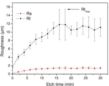
Another approach to estimate SSD depth using acid etching is the interpretation of roughness profile as a function of etched thickness. This principle was already detailed elsewhere [22]. Figure 2 presents a roughness profile as a function of etched thickness obtained on a D64-ground fused silica sample (same sample as presented Fig. 1(b)).
(C) 2009 OSA 26 October 2009 / Vol. 17, No. 22 / OPTICS EXPRESS 20452
Fig. 2. Roughness profile evolution during HF etching for a D64-ground sample
Roughness is measured using a PHYNIX TR200 stylus profilometer. Values are obtained with 16 measurements equally placed radially on the surface with a scanning length of 4 mm. Incertitude is given at one standard deviation. Rt is computed on the whole set of 16
measurements. We observe the increase of the roughness and a plateau is reached. The SSD depth is estimated by the higher value of roughness Rt of this plateau: Rtmax = 16 µm.
2.3 SSD measurement by MRF dimpling, MRF taper
MRF is a sub-aperture polishing process that takes advantage of the properties of a magnetorheological fluid. Where classical finishing processes are dominated by normal load, MRF material removal is mainly dominated by shear load. It thus induces very low subsurface damage. Therefore, instead of using a steel ball to generate dimples, a MRF machine can be used to make the dimple when trying to reveal SSD by a local material removal. This principle was subsequently detailed by Randi [18]. We basically used the same method. Dimples were made on a Q22-X MRF polishing machine from QED (QED Technologies, Inc., Rochester, NY) in no rotating motion mode. 4 spots of identical depths were made on each sample to characterize. The depth of the dimple was chosen to be superior to the SSD depth thanks to an estimation based on Miller's law linking surface roughness with SSD [19]. Surface was then lightly etched during one minute to open cracks and ease microscope observations using an HF / HNO3 (80/20%v.) solution.
Each dimple was measured and observed using a nano-scratch tester from CSEM Instruments. This apparatus is equipped with a scratch head assembly unit coupled with an optical microscope optical head and an AFM unit. An X-Y motorized table allows the measurement of the same area of a sample under each unit. The principle of the measurement is to measure the dimple's profile, locate the position where transition between SSD and bulk material occurs with the optical microscope and compute the corresponding depth (see Fig. 3).
(C) 2009 OSA 26 October 2009 / Vol. 17, No. 22 / OPTICS EXPRESS 20453
Fig. 3. MRF dimpling principle
Dimple profile measurement is performed by making a single scratch test across the dimple with a 1mN contact force of the diamond tip. The displacement speed of the sample is set to 10mm/min. These parameters are adequate to maintain contact in the dimple between diamond tip and sample without marking the sample. The penetration depth of the diamond tip during scanning is then computed by the nano-scratch tester.
SSD transition is
visualized along the scanned profile to determine the SSD depth at the
position of the last visible crack
. A typical image of a transition between SSD and bulk material such as observed under an optical microscope is presented in Fig. 4.Fig. 4. Optical microscope image of a MRF dimple showing SSD transition (1 graduation = 80µm) – D64 machined fused silica sample. The doted line indicates the position of the last visible crack giving the depth of the SSD
We also performed MRF taper polishing to measure the SSD on samples. The MRF taper polishing was performed at QED on an area of 8 cm x 8 cm. Maximal depth was adapted to the roughness of the sample to measure. Sample was then etched during one minute in a HF / HNO3 (80/20%v.) solution to open cracks. Observation was carried out on a REICHERT
microscope equipped with a X-Y translation stage in Nomarski mode; SSD depth is obtained when the last crack is observed as going down inside the taper. Alternatively, we also used a confocal LEICA DMR SP2 to observe SSD in fluorescence mode; such a system was already described and successfully used in a previous work to measure SSD on dedicated specifically manufactured samples [23].
3. Results and discussions
Samples detailed in section 2.1 were measured using the techniques detailed in section 2.2 and 2.3. It must be outlined that it is not possible to combine all the different SSD measurement methods on the single side of a given sample since most of them are
(C) 2009 OSA 26 October 2009 / Vol. 17, No. 22 / OPTICS EXPRESS 20454
destructives. For example, MRF dimpling can't be combined with HF bath dissolution & ICP since MRF pollutes the optics with polishing abrasives, MRF taper uses almost the whole side of the optic and thus cannot be done on of the same side of an MRF dimple, etc. The results obtained are given on Table 5.
Table 5. Comparison of different SSD measurements methods on various diamond ground samples. For the MRF taper method, both Nomarski and confocal microscopy
evaluations are given. All quantities are expressed in microns.
S/N 9.1 Rt [19] MRF Dimpling HF dissolution & Roughness HF dissolution & ICP MRF taper microscopy / confocal S1 119.02 111.1 - - - S2 87.99 - 117.9 110 - S3 26.93 24.2 - - - S4 26.39 - - - 21 / 28 S5 21.84 - 20.4 25 - S6 55.69 51.9 - - - S7 56.23 - 35.7 52 - S8 2.64 - - - 2 / 2 S9 11.19 - 9.3 14 - S10 12.01 - - - 7 / 10 S11 8.55 - 8.2 9.5 -
Some comments came be made regarding the obtained figures. The SSD evaluation made from the Rt measurement [19] gives a first good estimation. Some odd values can be denoted
on sample S2 (9.1 Rt) and sample S7 (HF dissolution & roughness). We believe these low
numbers are due to the imprecision of the evaluation of the roughness p-v. Measurement of this value is very sensitive to scanning length and position on the sample. To limit this imprecision, we have chosen to use a large number of measurement on the sample (16) compared to previous work [19,20] but it is still insufficient to ensure a good Rt evaluation.
Regarding MRF taper measurement, we can also underline that confocal microscopy observation give always a larger depth that classical microscopy. This is due to the superior resolution of the techniques and its ability to see subsurface unopened cracks has been demonstrated before [21]. Finally, the HF dissolution & ICP method, which is the only one that did not use a roughness measurement, delivers depths in good correlation with the 9.1Rt
since deviation of no more than 23% is found.
4. Conclusion
We manufactured diamond ground fused silica samples using various diamond grinding wheels from D181 down to D20. The SSD of these samples was measured using five different principles. We evidenced a rather good correlation between the measured depths since depths deviate no more than 20 to 30% from one another. We believe that most of this discrepancy is induced by the evaluation of the roughness p-v (Rt) which is in nature dependant on the area
and measuring conditions. To overcome this problem, we introduced a new SSD measurement principle using the decreasing of contaminants analyzed by ICP-AES during HF etching. Depending on the part interface contamination, this method can also use a Ba marker to enhance its sensitivity. We demonstrate that this method delivers depth in good concordance with evaluation made from the 9.1 Rt law. To conclude, if etching can provide a
means to convert SSD into roughness [22], it can also be a valuable tool to measure subsurface damage particularly when coupled with ICP-AES. Since ICP-AES is a rather expensive technique, its usage is of interest for the development of a peculiar process with a one-time-only test before going into production. We also underline that the method can be extended to other optical materials than fused silica as long as there etching is isotropic. It is for example the case of BK7, Zerodur or silicon that are material of particular importance in optical workshops.
(C) 2009 OSA 26 October 2009 / Vol. 17, No. 22 / OPTICS EXPRESS 20455
Acknowledgments
This work is supported by the Conseil Régional d’Aquitaine and is performed in the framework of the EFESO project.
(C) 2009 OSA 26 October 2009 / Vol. 17, No. 22 / OPTICS EXPRESS 20456