HAL Id: hal-00740788
https://hal.archives-ouvertes.fr/hal-00740788
Submitted on 24 Mar 2020HAL is a multi-disciplinary open access
archive for the deposit and dissemination of sci-entific research documents, whether they are pub-lished or not. The documents may come from teaching and research institutions in France or abroad, or from public or private research centers.
L’archive ouverte pluridisciplinaire HAL, est destinée au dépôt et à la diffusion de documents scientifiques de niveau recherche, publiés ou non, émanant des établissements d’enseignement et de recherche français ou étrangers, des laboratoires publics ou privés.
Boron-deuterium complexes in diamond: How
inhomogeneity leads to incorrect carrier type
identification
Amit Kumar, Julien Pernot, Franck Omnès, Pierre Muret, Aboulaye Traoré,
Laurence Magaud, Alain Deneuville, Nada Habka, Julien Barjon, François
Jomard, et al.
To cite this version:
Amit Kumar, Julien Pernot, Franck Omnès, Pierre Muret, Aboulaye Traoré, et al.. Boron-deuterium complexes in diamond: How inhomogeneity leads to incorrect carrier type identification. Journal of Applied Physics, American Institute of Physics, 2011, 110 (3), pp.033718. �10.1063/1.3611035�. �hal-00740788�
Boron-deuterium complexes in diamond: How inhomogeneity
leads to incorrect carrier type identification
A. Kumar, J. Pernot,∗ F. Omn`es, P. Muret, A. Traor´e, L. Magaud, and A. Deneuville
Institut NEEL, CNRS and Universit´e Joseph Fourier BP166, 38042 Grenoble Cedex 9, France
N. Habka
Groupe dEtude de la Mati`ere Condens´ee (GEMaC), Universit´e Versailles St. Quentin, CNRS, 1 Place Aristide Briand, 92195 Meudon, France
CEA, LIST, Diamond Sensors Laboratory, F-91191 Gif-sur-Yvette, France. J. Barjon, F. Jomard, M.A. Pinault, and J. Chevallier
Groupe dEtude de la Mati`ere Condens´ee (GEMaC), Universit´e Versailles St. Quentin, CNRS, 1 Place Aristide Briand, 92195 Meudon, France
C. Mer-Calfati, J.C. Arnault, and P. Bergonzo
Abstract
The electrical properties of boron doped diamond layers after deuterium diffusion have been in-vestigated by Hall effect and capacitance voltage measurements. It is found that i) the deuterated boron doped diamond layers are inhomogeneous after the deuterium diffusion resulting in conduct-ing and insulatconduct-ing area, ii) negative and positive Hall voltage are measured on the same boron doped sample after deuterium diffusion depending of the contacts geometry (negative with van der Pauw and positive with mesa etched Hall bar), iii) in the conducting area, the majority of the boron-deuterium complexes are not ionized after the deuterium diffusion. The detailed electrical measurements using mesa-insulating Hall bar structures revealed that the existence of inhomoge-neous regions with conducting and insulating areas is the most probable source of wrong n−type conductivity in deuterated boron doped diamond layers of this work. In the light of this result, the possibility of an incorrect assignment of a shallow donor previously reported in deuterated boron doped diamond is discussed. Finally, confirmation is given that the boron deuterium complexes created after the deuterium diffusion are neutral in p−type diamond.
I. INTRODUCTION
The continuous progresses in the crystal growth and doping of diamond make it a key material for manufacturing high-power, high-temperature and high-speed electronic devices for the forthcoming years. p−type doping is now well mastered by incorporation of boron atoms during the growth leading to an acceptor at 380 meV above the valence band. Large doping level range is now possible (from 1014cm−3 to few 1021cm−3 ) opening the way for the
fabrication of unipolar devices like Schottky diode or field effect transistor1,2. n−type doping
is more difficult due to the elevated ionization energy of phosphorous (P) donor at 570 meV below the conduction band3. Koizumi et al.4 demonstrated, for the first time, the possibility
to dope homoepitaxial diamond layers with P atoms using {111}-oriented substrates. Some other groups were then able to reproduce the same doping process5–7. Recently, Kato et al.8
succeeded to dope{100}-oriented homoepitaxial diamond in spite of the difficulty of P-atoms incorporation for this crystal orientation. These progresses lead to the possibility to perform some bipolar diamond based devices but generally with a high serial resistance due to the low density of electron in the n−type layer. In 2003, Teukam et al.9 discover the possibility
to get n−type material using boron doped diamond after a deuterium plasma diffusion. The authors proposed that boron-deuterium (BD2) complexes could be at the origin of a
shallow donor level with an ionization energy in the range of 230 to 370 meV, which is the range of the thermal ionization deduced from the temperature dependence of the electron Hall electron density9–12. Even if few boron doped samples exhibit negative Hall voltage
after deuterium diffusion, the understanding of the origin of this n−type conductivity is still missing and no other experimental proof than Hall effect using the van der Pauw contact geometry of the electron transport has been given. Theoretician groups investigated the electronic properties of BHn complexes in diamond and concluded that no shallow donor
levels close to the conduction band are induced by such kind of complexes13–18. Ab initio
calculations are performed using H atoms indeed D but the ab initio results are expected to be same with D atoms. A clear picture about the origin of the n−type conductivity in deuterated boron doped diamond is still missing .
The aim of this work is to investigate the electrical properties of boron doped samples after deuterium diffusion using different electrical measurement techniques (temperature de-pendent Hall effect and capacitance-voltage measurements) and test patterns (Hall bars with
mesa etching, van der Pauw squares without mesa etching or ring-shape Schottky diodes) in order to improve the understanding of such doping. The paper is organized as follow: in a first part, the experimental details about the six samples preparation and measurement techniques (Hall effect, capacitance voltage and secondary ion mass spectrometry) are given. In a second part, the temperature dependent Hall effect measurements performed on the deuterated boron doped samples are analyzed and a mobility study is performed in order to determine the charge state of the complexes created by the deuteration process. Finally, a discussion is given about the possibility to measure wrong n−type due to the non homo-geneity of boron doped layer after deuterium diffusion and about the charge state of the (B,D) complexes. The paper is concluded by a brief summary.
II. EXPERIMENTAL DETAILS
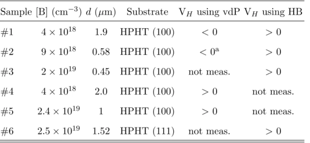
Six boron-doped layers were grown by microwave plasma enhanced chemical vapor de-position at CEA-LIST on Ib (100) (for samples #1 to #5) and (111) (for samples #6) High Pressure High Temperature-grown (HPHT) 3 mm by 3 mm diamond substrates from Sumitomo Electric. The atomic boron density and the thickness of the homo-epitaxial layer have been measured by secondary ion mass spectrometry (SIMS) (an example is shown for sample #1 in Fig 1). The boron content ranges between 4 × 1018 cm−3 and 2.5× 10¹⁹
cm−3. Table I summarizes the structural characteristics of the six samples investigated in this work. These boron-doped samples were then exposed to a microwave deuterium (D) plasma at 550◦ C for duration of 30 minutes to 8 hours (depending on the thickness and the
doping level) at a deuterium pressure of 10 torr at N´eel Institute. The D profile has been checked systematically by Secondary Ion Mass Spectrometry after each deuteration. Deu-terium has been used instead of hydrogen in order to have a lower detection limit by SIMS. The deuterium diffusion process have been reproduced as many times as needed to reach the condition [D] in the same range than [B] (equal or larger in the whole epilayer thickness). Then, two kinds of metallic contacts geometry were used: van der Pauw squares without etching (vdP) were simply evaporated in the middle or in the corner of the samples and Hall bars (HB) were done using a six steps technology process (with UV lithography and O2
ECR etching for the epilayer insulation). It must be noticed that the area where the carrier density is measured on the Hall bar has not been exposed to UV light during the process.
The Hall bar geometry results in a 180 µm times 450 µm rectangular area. The van der Pauw geometry is a square of metallic contacts. Each contact are squared surface of 100 µm by 100 µm separated by 400 µm (distance from the center of each square contact). To avoid the thermal dissociation of (B,D) complexes9,10, no annealing of the Ti/Pt/Au metallic
con-tacts were performed during or after the vdP or HB processes. Surface conduction channels were avoided by oxidizing the sample surface by acid treatment prior to any electrical mea-surement. Hall effect measurements were performed under well controlled conditions within the temperature range of 280 K to 520 K. The I(V ) characteristics of the contact were not systematically perfectly ohmic due to the absence of annealing to create the carbide with Ti but enough conducting to inject the current needed for Hall effect measurement. Hall effect and resistivity measurements were carried out with a high input impedance system using an a.c and d.c. magnetic field B with a maximum amplitude of 0.8 T (0.4 T in the case of a.c.) in the standard configuration (i.e. B, the magnetic field, parallel to the growth axis and j, the current density, perpendicular to the growth axis). Ring shape Schottky diodes were then fabricated using Al for the Schottky metal (200 µm diameter) and the Ti/Pt/Au for ohmic contacts. C(V ) measurements have been performed to evaluate the depth profile of the active boron acceptors in the layer. The frequency of measurement used for C(V) was adapted to the RC constant of each sample in order to get the best signal over noise ratio (between 1kHz and 10 kHz) .
III. RESULTS
A. Temperature dependent Hall effect measurements after deuterium diffusion.
Two kinds of contact geometry has been used in this work in order to investigate the electrical properties of the deuterated boron doped layer (vdP and HB). It must be noticed here that the vdP geometry described above and used in this work deviated from the one intended by van der Pauw in his original work19. Indeed, van der Pauw method is based
on a configuration where metallic contacts are placed in the periphery of the sample and/or isolated by a mesa-etched structure. These requirements insure a reliable resistivity and Hall effect measurements. This is not the case of the vdP without mesa patterns used in the present work.
1. Passivation of boron acceptors by deuterium atoms.
Four of the six samples have been measured to be p−type after the deuterium diffu-sion process, two using a HB (samples #3 to #6) and two using a vdP ( #4 and #5). The temperature dependence of the carrier concentration exhibit a slope characteristic of the ionization energy of the boron acceptor. The Hall carrier concentration pH(300K) at
300 K were measured at 7× 1013cm−3 (sample #3), 6× 1014cm−3 (#4), 1012cm−3 (#5) and
1016cm−3(#6). Assuming a total electrical activation of the boron atoms measured by SIMS
in the diamond matrix (boron atoms are all substitutional boron [BS]=[BSIM S]=[B]=NA),
this corresponds to a ratio between free hole density per boron acceptor (pH(300K)/NA)
of respectively 3.5× 10⁻⁶, 1.5× 10⁻⁴, 4.1× 10⁻⁶, and 4× 10⁻³. The ratio p
H(300K)/NA
of samples #3-#5 are lower than that generally observed for this doping range (see for example20,21). Only the sample #6 is in the usual range. However, the carrier density
tem-perature dependence after deuterium diffusion shows that the conduction is governed by an impurity band or hopping conduction leading to an overestimation of this ratio at room temperature. The ratio pH(300K)/NAof the four samples is easily explained by an
overesti-mation of the electrically active boron atoms [BS]=NA in the diamond matrix since a large
fraction of these atoms are passivated by deuterium atoms as previously reported22–31. This
passivation of boron by deuterium or hydrogen is well known and expected. The passivation efficiency is clearly sample dependent but without understanding for the physical meaning at this moment. Moreover, it is important to notice that van der Pauw patterns have been done without insulating mesa and so can lead to incorrect resistivity value determination. So in these cases, it is hazardous to compare sample to sample or sample before and after deuterium diffusion due to approximative quantitative measurements.
2. Samples with opposite sign of the Hall voltage using the two different test patterns HB and vdP.
Two samples (#1 and #2) show opposite sign of the Hall voltage after deuterium diffu-sion on the same sample depending if the measurement is done with a vdP or a HB.
configuration where a SIMS crater is located inside a 400 µm by 400 µm van der Pauw pattern, this pattern being far from the borders of the sample. The SIMS crater results in an hole of 100 µm by 100 µm square in the whole depth of the epilayer. The Hall con-centration temperature dependence is reported on Fig. 2. In this particular van der Pauw geometric configuration, a negative Hall voltage (n-type) is measured in the whole range of temperature. The signal is very noisy and has a thermal activation close to the one of the measurements done with HB. On the opposite for HB, the Hall voltage is positive (p-type) and not noisy. The thermal ionization is characteristic of the boron acceptor.
Recently, Ohgaki et al. obtained positive Hall coefficients from contact misplacement on evident n-type ZnO films and crystals32. In order to explain these results, Bierwagen et al.33
investigated the role of inhomogeneities in carrier concentrations and show that it can result in an incorrect identification of the carrier type when using a square-shaped sample with contacts inside the sample area. Yom-Tov34 observed the same phenomenon in B-doped
homoepitaxially grown diamond in the as-grown state and following oxygen reactive ion etching using also a finite element simulation to investigate the role of inhomogeneity.
In the case of a square hole in the middle of the contacts, Bierwagen et al. found that when the distance ratio between the two closest contacts and the side length of the squared sample is lower than 0.45, an incorrect identification of the carrier type is obtained. The negative ratio between the actual carrier density (the one that we should measure without inhomogeneity) and the measured one (with inhomogeneity) decreases strongly in the negative values when the ratio of the distance between the two closest contacts and the length of one side of the squared sample increases. Our experimental configuration is very similar with a SIMS crater located between the contact pads. In this case, the negative Hall voltage measurement is certainly not due to an inversion of carrier type conduction (n-type in this case) but due to an incorrect identification of the Hall voltage sign due to the distortion of the potential distribution arising from the inhomogeneity induced by the crater. The Hall effect performed with the help of a mesa-isulating HB is known to be reliable and so we can consider that the measured data reported on Fig. 2 correspond to the correct sign and density of the Hall carrier. As observed on Fig.2, the ratio r between the hole concentration measured using the HB and the carrier concentration measured with the vdP configuration including the SIMS crater leads to a value of about -0.1. In order to get
a quantitative study, the procedure proposed by Bierwagen et al.35 based on the software
FREEFEM++36has been adapted to our exact experimental case. The calculation confirms
the inversion of the sign of the Hall voltage due to the inhomogeneity induced by the presence of the SIMS crater and a ratio r of -0.05 was found for B=0.5 T. It should be noticed that the vdP and HB were not performed at the same area and so an inhomogeneity of the doping level after deuteration (inhomogeneous passivation of the boron atoms for example) can contribute to the absolute value of the measured carrier concentration ratio r between HB and vdP independently of the effect described in ref 33. This resistivity inhomogeneity can participate to the inversion of the sign but should be less influent that the SIMS crater which has an infinite resistance on a 100 µm × 100 µm square area in a 400 µm × 400 µm vdP area. This experimental measurement of an incorrect determination of the Hall voltage sign due to an inhomogeneity shows that the predictions of Bierwagen et al.33is correct and
so, for the determination of the carrier type (n or p), it is clearly more reliable to use a Hall bar with a mesa etching in order to force the current lines to stay in between the Hall voltage probes. Considering the carrier concentration measured with the HB, the calculation of the ionization ratio (pH(300K)/[B]) gives 2× 10⁻⁴ which here also is overestimated due to the
parallel conduction at low temperature. For this sample also, a partial passivation of the boron atoms is obtained.
Concerning sample #1, the Hall effect and resistivity measurements have been performed using a vdP far from the borders of the sample and a HB in the same location of the sample as the vdP. An area of about 100 µm by 100 µm was common to the two patterns (square of the vdP and rectangle of the HB) which is mainly localized below one squared contact of the vdP and in one extremity of the HB (the 100 µm by 100 µm surface was measured by superposition of two microscope pictures with the vdP and HB patterns). No SIMS crater was present neither in the HB nor in the vdP area. The Hall carrier concentration and mobility temperature dependence are reported on Fig. 3. The measurements done with vdP result in a negative Hall voltage (n-type) in the whole range of temperature. At the opposite for the HB, the Hall voltage is positive (p-type). The signals are not noisy and the Hall voltage exhibits a linear behavior with the injected current and the magnetic field for the two geometries. Two possible situations could explain the difference of carrier type (n and p) on the same sample with two different patterns: i) the carrier type is not homogeneous due to a majority of donors in some area (the vdP area) and a majority of
acceptors in some others (the HB area), ii) the vdP patterns gives an incorrect type of carrier (false n-type identification which is in fact p−type) due to a local inhomogeneity in the vdP area. Our experimental data show that the second possibility is the most relevant. First, a 100 µm by 100 µm square under one of the voltage probe contact of the HB has been fabricated on the area delimited by the vdP pattern. If the area under the contact is actually n-type, since the other voltage probe contact of the HB are fabricated on a p-type material, the I(V) measurement between two contacts (with one of the two which is on the vdP area) must exhibit a rectifying behavior characteristic to a pn junction. The measured I(V) characteristics are not rectifying. Second, the resistivities of the two area exhibit the same temperature dependence. If we consider the first possibility, even if the ionization energy of the two impurities (boron acceptor in p-type region and shallow donor in n-type region) could be close, the electronic properties of each band (the valence band and the conduction band), like the effective mass for example, should involve a difference in the temperature dependence of the resistivity which is not observed. The resistivity temperature dependence of sample #1 with HB and vdP are similar to the ones of sample #3 and sample #4. The hole mobility measured in the p−type region using the HB is in very good agreement with typical mobility usually measured in lightly doped samples. At high temperature, the intrinsic scattering mechanism by optical phonon governs the mobility with a slope and a magnitude previously observed in other boron doped samples37,38. At the
opposite, the temperature dependence of the mobility measured in the n-type area using the vdP does not decrease with the characteristic power law (T−α) generally observed for the
electron mobility39,40 at high temperature, when the mobility is governed by the intrinsic
phonon scatterings. Third, local non homogeneity are measured using the HB patterns. Indeed four different HB have been performed on the sample #1. Only one of the four HB exhibits ohmic behavior between the metallic contacts of the HB. The three others were non-ohmic or completely insulating (no current injection possible) demonstrating a strong inhomogeneity of the material under the metallic pads. The ohmic HB were built in a way which permits to measure the sheet resistance (using 4 probes) of two adjacent area (125 µm by 180 µm for each area) leading to different values of 31 kΩ for one and 82 kΩ for the other one.
In summary, the resistance measurements performed on the HB of sample #1 show a strong inhomogeneity in the deuterated sample. The Hall voltage seems to be incorrect in
the vdP configuration. This is attributed to these inhomogeneities and to the use of vdP not located in the corners of the sample. The mobility, deduced by a combination of the two measurements, confirms, from its temperature dependence and magnitude, the incorrect determination of the Hall voltage. The incorrect carrier type identification is supported by the fact that the ionization energy deduced from the n-type measurements is similar to the boron ionization energy. Even if the sign and the magnitude of the Hall voltage are incorrect, the thermal ionization should be more or less the one of boron acceptor. The slope of the carrier concentration temperature dependences of Fig. 3 results in an estimate of the ionization energy of 245 meV for the vdP and 181meV for the HB. These values are in the same range that to the ones attributed to the shallow donor9–12 but far from the
ionization energy of the Boron acceptor (380 meV). However, the correspondence between the slopes determined from the fit of the carrier concentration versus temperature on two decades of Fig. 3 is approximative since it doesn’t take into account the compensation of the semiconductor. For a more accurate determination of the ionization energy, the Boltzmann statistics in doped and compensated semiconductor must be used41. p
H(T )
increases versus T with an exponential law and the plot of ln(pH(T)/NV) versus 1/T has a
slope EA up to a concentration close to, but below, the compensating donor concentration
(ND). In this equation, NV is the equivalent valence band density of state with a T3/2
temperature dependence. Then, for pH higher than ND but much lower than NA-ND, the
slope of ln(pH/NV) versus 1/T decreases to reach EA/2. For pH(T ) in the range of NA-ND,
the exhaustion regime occurs and the slope tends to zero. This can be observed on the pH temperature dependence of a low boron doped diamond epilayer reported on Fig. 3
(sample #2 of Ref 37). In this case, ND is equal to 1.5× 1015 cm−3 and the boron acceptor
concentration 1.7× 1016 cm−3. The exhaustion regime is not achieved in this temperature
range. So, when the temperature range of measurement is sufficiently large to measure a variation of pH on more than 3 or 4 decades variation, it starts to be possible, using
the neutrality equation and comparing with the experimental data, to determine the three unknown impurity parameters : EA, NA and ND. This is well illustrated for example in
the case of n−type 4H-SiC42. As shown on Fig. 3, the carrier density of sample #1 using
a HB of this work and the sample #2 of Ref 37 are exactly the same for carrier densities higher than 1015cm−3 with a slope of E
A/2 typical of boron acceptors. Then, when the hole
to EA but the slope of sample #1 remains at EA/2. This means that the compensation
density ND in sample #1 is smaller than the lowest hole density (6× 1013 cm−3) measured
at the lowest temperature (room temperature) since no kink is observed on the slope. This shows that deuterium passivates both the acceptors and the compensating donors. Also, for sample #1, the actual ionization energy of the dopant is 362 meV which is two times 181 meV (the one observed from the slope of ln(pH(T)/NV)) in good agreement with the boron
acceptor ionization energy.
Also, if the fit of pH(T) is done in a reduced range of pH variation which doesn’t permit
to observe a clear kink (this is the case here for sample #1 and Refs. 9–12), the determined value of the ionization energy will be EA if the pH �ND, EA/2 if the pH �ND and an
ionization energy between EA and EA/2 if pH is in the range of ND. This could explain
the ionization energy assigned to the shallow donor (230 to 370 meV) in Refs.9–12 if the identification of n−type is wrong due to non homogeneity and in fact due to boron acceptor ionization energy43. Indeed, in this case, the compensation density was not known and the
carrier density variation range (2 decades) not sufficient to observe a clear kink.
For sample #1, a detailed microscopic picture of the inhomogeneity localised in the vdP contact area is needed in order to simulate the potential distribution and to perform a quantitative analysis of the non homogeneity effect on the Hall voltage. The electrical inho-mogeneity of this sample has been measured with patterns of typically hundred micrometers squared which is not sufficiently small to get an accurate picture of the resistivity mapping.
B. Charge state of the (B,D) complexes and their effect on the mobility of free holes.
In this section, the charge state of the (B,D) complexes and their effect on the mobility of free holes are investigated. The sample #1 is initially doped at a level of [BSIM S]=4×
1018 cm−3. Capacitance voltage measurements have been performed on sample #1 using
a Ti/Pt/Au ohmic contact surrounding nine circular Al contacts (200 µm diameter) in order to obtain a rectifying behavior. The gap between the two electrodes was 20 µm. Seven among the nine contacts were ohmic. The two others show some current-voltage I(V) characteristics with a ”rectifying” behaviors but with only one decade between the reverse and forward bias at -20 V and +20V. The two circular contacts are separated by a distance of
400 µm (distance separating the centers of two successive diodes). The ”rectifying” behavior of the two diodes are opposite (one p-type like and one n-type like). Capacitance voltage C(V) measurements were performed on the two diodes Fig. 4a. Concerning the n-type like diode from I(V), the C(V) characteristic corresponds to an insulating diamond layer of 20 µm thickness. The capacitance is almost not varying with the reverse voltage and so, the whole diamond between the two electrodes (20 µm gap) is insulating resulting in a value close to 60 fF. Also, the ”rectifying” behavior of the I(V) characteristic cannot be assigned to a Schottky diode on a n-type material. This corresponds to the passivated layer observed by Zeisel et al23 below the diamond surface but in this case in the whole gap of
the Schottky diode. Concerning the p-type like diode by I(V), the C(V) measurement is characteristic of a Schottky contact on a p-type low boron doped diamond with a space charge variation versus reverse bias. The linear behavior of the I(V) curve in the forward regime leads to a series resistance of 2 MΩ. This high series resistance could be at the origin of some wrong quantitative analysis when using the parallel equivalent model (capacitance and conductance in parallel)44,45. In order to prevent such kind of misinterpretation, a low
frequency signal of 1 kHz has been used in order to get a measured dissipation factor DP44,45
below 0.2 for reverse bias between 0 V and 8 V and between 0.2 and 0.3 for 8 V to 10V. Then, from the inverse squared capacitance 1/C2 versus voltage of this diode, a doping level
of 2× 1015 cm−3 is deduced from the slope as shown on Fig 4b. It must be noticed that
this value is an evaluation since the extension of the space charge region is assumed to be cylindric within the epilayer and that is not the exact situation. Indeed, the extension (from 2 to 2.5 µm if considering cylindric extension) exceeds the epilayer thickness and a lateral extension occurs when the space charge due to Schottky contact links with the one due to Ib-substrate(n)/epilayer (p) junction. However, the order of magnitude of the deduced net boron doping is not affected by that assumption.
Comparing the net active acceptor NA-ND measured by C(V) on the p−type Schottky
diode with the boron atoms concentration measured by SIMS, we deduced that approxi-mately one over two thousands of the boron atoms in diamond crystal which are electroni-cally active after the deuterium diffusion process. Two situations could explain this ratio. First, the compensating donor concentration ND is lower but in the range of the boron
ac-ceptor in substitutional site NA which writes NA�ND. In this case, the origin of the donor
should be ionized since each donor capture one hole from the NAacceptor. Second
possibil-ity, the huge majority of the boron atoms in this sample interacts with D to create a deep acceptor which is neutral and makes electrically inactive the boron acceptor. From these two possibilities, one major difference appears which is the charge state of the 4× 1018cm−3
(B,D) complexes. A signature of this large concentration of ionized or neutral impurities should be detectable from transport measurement. Since the low temperature mobility is very sensitive to the ionized impurities, the temperature dependence of the hole mobility has been examined using the two different assumptions (neutral or ionized impurities). In order to calculate the mobility in boron doped diamond, we used the procedure described in Ref. 38 which is efficient to distinguish the neutral from the ionized impurity scattering. The mobility calculation is based on the relaxation time approximation and take into ac-count the free hole scatterings by impurities (neutral or ionized) and phonons (acoustic and optic). A net acceptor NA-ND concentration of 1016cm−3 is assumed to evaluate the carrier
concentration temperature dependence. This value is estimated from the extrapolation of the temperature dependence of the carrier concentration of Fig. 3 a in the HB case with mesa-insulation. The phonon-hole interaction constants (acoustical potential and optical coupling constant) determined in Ref. 38 are introduced to describe the high temperature dependence of the mobility. The phonon contribution to the total mobility is shown on Fig. 5 as a joined contribution of the acoustic phonon (ac) and optical phonon (op).
For the low temperature range, the two possibilities have been considered: i) the (B,D) complexes are ionized and so, we introduce 4× 1018 cm−3 ionized centers for the ionized
impurity scattering (ii), ii) the (B,D) complexes are neutral and so, we introduce 4× 10¹⁸
cm−3 in the neutral impurity scattering (ni). In the first case, the contribution of the ni
mode is negligible on the total mobility. In the second case, the contribution of the ii mode is negligible. The total mobility temperature dependence for the two cases are shown on Fig. 5. In the first case, the ii mode joined to the phonon contribution (ac+op mode) results in a mobility which is clearly too low in comparison with the experimental data. This disagreement shows clearly that the (B,D) complexes are not ionized (positively or negatively). In the second case, the ni scattering joined to the phonon scattering gives a mobility in good agreement with the experimental one. However, it must be noticed that the neutral impurity scattering used is from the Erginsoy model46. In this model, the impurity
have a very deep level in the band gap. In order to give a better quantitative description of the neutral impurity scattering, the model proposed by Meyer and Bartoli should be used which takes into account the incident energy of the hole47. The important physical parameter of this scattering mechanism is the binding energy of the hole to the impurity (see for example core impurity correction effect in Ref. 48). In our case, the binding energy of the scattering centers (neutral (B,D) complexes) is unknown and can not be introduced in the calculation. However, the fact that the binding energy of the scattering centers should be high, due to the depth of the (B,D) complex level, should result in a lower cross section than the one used in the Erginsoy model46 and consequently to a lower efficiency
of the scattering mechanism. This could explain why the calculated mobility seems to be underestimated in comparison with the experimental one due to an underestimation of the ni scattering. The comparison between the experimental data and calculated mobility is in good agreement in the high temperature range where the scattering is dominated by the intrinsic phonon scattering. The most important result is that the (B,D) complexes created after the deuterium diffusion are not ionized in the p−type diamond.
IV. DISCUSSION.
Recent theorist groups have investigated the (B,D) complexes in diamond in order to establish the origin of the n−type shallow donor level13–18. Yan et al.15 proposed that the
n-type conduction occurs in a BH impurity band with the BH2 centers acting as dopant
of this impurity band. However, even if the concept is original and interesting, the elec-tronic properties of the BH and BH2 centers are not matching with the theoretical situation
proposed in this paper as discussed in Ref 16 and 17. Dai et al49 calculated the electronic
properties of the different BHncomplexes and concluded about the possibility to get n−type
conductivity. However, the small size of the cell used in their work could explain why they obtain a n−type conductivity. In their calculation, the defect concentration is huge (5×10²¹
cm−3) and induces an artificial defect-defect interaction. A good agreement is obtained in the literature to assign the BH pair to a deep acceptor level at about EC-1 eV13,16,17 and
the BH2 to a deep donor at about EC-2.7 eV13,16,17. These levels cannot explain a n−type
conduction with an ionization energy in the range of 0.23 to 0.37 eV from the conduction band. Recently, Lombardi17 investigated the properties of the metastable states of the BH
and found that this deep donor has some metastable states resulting in a shallower ioniza-tion energy (0/+) than the most stable but still too deep (EC-0.8 eV for the shallowest) to
match with the one observed experimentally9–12.
The experimental data of this work are in good agreement with the theoretical predictions concerning the BH pairs. If the BD pairs are created during the deuterium diffusion process and if we neglect the BDn complexes, the doping level induced by the boron acceptor in
substitutional site [BS] without bonded hydrogen should decrease in the same proportion
than the BD pairs are forming. The decrease of the acceptor level after the deuterium process is observed in this work and in previous works9,22–26.
The fact that the sample can be measured to be p−type after the deuterium diffusion process but with a low doping level (lower than few 1016 cm−3) indicates that the BD pairs
are not donors. Actually, BD pairs are deep acceptors according to theorists and should be neutral centers in p-type diamond. This is in good agreement with the mobility analysis since in this case they can acts as neutral center and don’t compensate the substitutional boron acceptors. The BD pairs acceptor should be observable by deep level transient spectroscopy (DLTS) using an optical excitation in order to investigate deep levels near the conduction band at the opposite to the standard DLTS where only the deep levels near the valence band are measurable in p−type material50.
Concerning the BH2, the presence of such kind of complexes is expected when the [H] or
[D] measured by SIMS is twice higher than [B]. This is the case for sample #1 in the first 500 nm of the boron doped homoepitaxial layer in the area where the SIMS measurement have been done (cf Fig. 1). Anyway, the different boron deuterium related complexes could be present in the sample with different concentrations (isolated [BS], [BD] and [BD2]). If we
assume that the BD2 is a donor and we neglect the compensation due to other impurities or
defects, the BD2 should compensate the active boron acceptor and also the [BD] acceptor.
In this case, the area where [BD2]>[BS] +[BD], the material should be n-type but with a
so deep donor level that the material should be completely insulating. In the area where [BS]>[BD2], the material should be p-type and semiconducting. In the area where [BD]+[BS]
>[BD2] and [BD2]>[BS], the material should be p-type but with a majority of deep acceptor
(BD pairs) and so also insulating.
The two step deuteration process proposed by Chevallier et al.51for the donor formation
550◦C), with the deuterium forming B-D complexes that passivate the B acceptors. Further exposure to the D plasma leads to a further, faster diffusion of deuterium into the layer. Once a D/B ratio of 2 is reached the fully passivated (D/B = 1 containing layer) turns into the newly discovered n-type diamond layer. The formation of [BD2] proposed by Chevallier et
al.51seems to be in good agreement with the theoretical calculations performed for example,
by Lombardi17: the initial (slow) deuteration is governed by the trapping-detrapping of
deuterium at substitutional B atoms with a large activation energy of diffusion, while the second, faster, deuteration step will be governed by the trapping-detrapping of deuterium by BD pairs, with a small binding energy of 0.23 - 0.71eV, depending on the charge state. As a conclusion, in samples with [D]>[B], the formation of BD2 pairs acting as deep donors
can be considered as a possibility. However, more investigations are needed to prove their existence.
In this work, C(V) and Hall measurements clearly show that the boron doped epilayer are passivated but not homogeneously. Some area of the sample are insulating, some other are lightly p-type doped with different doping levels NA-ND. It was also the case in Ref.
12 where some non homogeneity has been found on the conductivity of the whole surface of the epilayer. The two step deuteration process is certainly influenced during the dif-fusion process by the impurities or defects present in the epilayer and so inhomogeneity of the sample itself before D diffusion. Some area of the sample could stay partially pas-sivated by D ([BD]>[BS]>[BD2]) and so p-type and semiconducting (incomplete one step
process). Some other areas could be partially in the second step process ([BD2]>[BD]>[BS]
or [BD]>[BD2]>[BS]) and so insulating. These non-homogeneities could result to an
in-correct carrier type identification from Hall measurement when using the van der Pauw pattern. This model explains i) why a strong non homogeneity of the resistivity is observed on the same sample after deuteration and ii) why a n−type like conductivity is observed as discussed above while the material remains p−type. This is certainly the case of the sample #1 using the van der Pauw pattern (p−type with the Hall bar) and in the work 12 where the van der Pauw contacts were far from the corners. In the other reports where the n-type conduction has been observed, the van der Pauw pattern without mesa were also used but with the contacts ”in the corner of the sample”9–11. However, a quantitative analysis of the
ratio between the length of two successive contacts and the length of the sample (square sample) would be necessary to evaluate the non homogeneity configuration that could
in-duce a wrong n-type identification in these samples. Anyway, a Hall bar or a van der Pauw pattern with a mesa etching is needed in order to reliably identify and to confirm a n-type conductivity in deuterated boron doped sample.
V. CONCLUSION
Several deuterated boron doped diamond layers have been investigated by mean of Hall effect (using Van der Pauw and pattered Hall bars) and capacitance voltage measurements. Boron doped diamond layers exposed to a deuterium plasma result in strong inhomogeneities of the resistivity on different areas of the same sample. Possible mechanisms of n−type conduction in deuterated boron doped diamond have been discussed to understand the controversial shallow donor level (n-type) in such diamond layers. A detailed electrical measurements using van der Pauw and patterned Hall bar structure revealed that the in-homogeneous conducting and insulating areas present in a given deuterated boron-doped diamond epilayer is the most probable source of wrong n-type conductivity in some deuter-ated boron doped diamond measured in past. Finally, it has been shown that the (B,D) complexes created after the deuterium diffusion are neutral in p−type diamond confirming previous conclusions.
ACKNOWLEDGMENTS
We thank Dr Pierre-Nicolas Volpe (Institut Neel, Grenoble, France and present address: CEA-LIST, Saclay, France) for the Hall bar process development, Mr Pierre Giroux of epitaxy group for the his support during the deuteration process (Institut Neel, Grenoble, France) and Mr. Bruno Fernandez of Nanofab (Institut Neel, Grenoble, France) for the fabrication of Schottky. We are thankful to Agence Nationale pour la Recherche (ANR programs: 06 BLAN 0339-02), France for providing financial support.
∗ julien.pernot@grenoble.cnrs.fr
1 R.S. Balmer, I. Friel, S.M. Woollard, C.J.H. Wort, G.A. Scarsbrook, S.E. Coe, H. El-Hajj, A.
2 P.N. Volpe, P. Muret, J. Pernot, F. Omn`es, Y. Koide, T. Teraji, F. Jomard, D. Planson, P.
Brosselard, N. Dheilly, B.Vergne, and S. Scharnholtz, Appl. Phys. Lett. 97, 223501(2010).
3 M. Katagiri, J. Isoya, S. Koizumi and H. Kanda, Appl. Phys. Lett. 85, 6365 (2004).
4 S. Koizumi, M. Kamo, Y. Sato, H. Ozaki, and T. Inuzuka, Appl. Phys. Lett. 71, 1065 (1997). 5 A. Tajani, E. Gheeraert, N. Casanova, E. Bustarret, J.A. Garrido, G. Rumen, C.E. Nebel, M.E.
Newton and D. Evans, Phys. Status Solidi A 193, 541 (2002).
6 M. Nesladek, K. Haenen, J. DHaen, S. Koizumi, and H. Kanda, Phys. Status Solidi A 199, 77
(2003).
7 T. Kociniewski, J. Barjon, M.-A. Pinault, F. Jomard, A. Lusson, D. Ballutaud, O. Gorochov,
J. M. Laroche, E. Rzepka, J. Chevallier and C. Saguy, Phys. Stat. Sol. a 203, 3136 (2006)
8 H. Kato, S. Yamasaki, and H. Okushi, Appl. Phys. Lett. 86, 222111 (2005).
9 Z. Teukam, J. Chevallier, C. Saguy, R. Kalish, D. Ballutaud, M. Barb´e, F. Jomard, A.
Tromson-Carli, C. Cytermann, J. Butler, M. Bernard, C. Baron and A. Deneuville, Nature Materials 2, 482 (2003).
10 R. Kalish, C. Saguy, C. Cytermann, J. Chevallier, Z. Teukam, F. Jomard, T. Kociniewski, D.
Ballutaud, J.E. Butler, C. Baron and A. Deneuville, J. Appl. Phys. 96, 7060 (2004).
11 C. Saguy, R.Kalish, C.Cytermann, Z. Teukam, J.Chevallier, F.Jomard, A.Tromson-Carli, J.E.
Butler, C. Baron, A. Deneuville, Diam. Relat. Mater. 13, 700 (2004).
12 C. Saguy, J. Chevallier, F. Jomard, C. Cytermann, B.Philosoph, R.Kalish, T. Kociniewski, D.
Ballutaud, C. Baron, A. Deneuville, Diam. Relat. Mater. 16, 1459 (2007).
13 J. P. Goss, P. R. Briddon, S. Sque, and R. Jones, Phys. Rev. B 69, 165215 (2004). 14 E. B. Lombardi, A. Mainwood, K. Osuch, Phys Rev B 70, 205201 (2004).
15 Y. Yan, Jingbo Li, Su-Huai Wei, and M. M. Al-Jassim, Phys. Rev. Lett. 98, 135506 (2007). 16 A. Kumar, J. Pernot, A. Deneuville, L. Magaud, Phys. Rev. B 78, 235114 (2008).
17 E. B. Lombardi, Diam. Relat. Mater. 18, 835 (2009). 18 E. B. Lombardi, Physica B 404, 4525 (2009).
19 L. J. van der Pauw, Philips Res. Reports, 13 1 (1958).
20 K. Thonke, Semiconductor Science and Technology, 18, S20 (2003).
21 T. Teraji, H. Wada, M. Yamamoto, K. Arima and T. Ito, Diamond Relat. Mater. 15, 602
22 J. Chevallier, B. Theys, A. Lusson, C. Grattepain, A. Deneuville, E. Gheeraert, Phys. Rev. B ,
58, 7966 (1998).
23 R. Zeisel, C.E. Nebel, M. Stutzmann, Appl. Phys. Lett. 74, 1875 (1999).
24 J. Chevallier, A. Lusson, D. Ballutaud, B. Theys, F. Jomard, A. Deneuville, M. Bernard, E.
Gheeraert, E. Bustarret, Diamond Relat. Mater. 10, 399 (2001).
25 C. Uzan-Saguy, A Reznik, C. Cytermann, R. Breuer, R. Kalish, E. Bustarret, M. Bernard, A.
Deneuville, J. Chevallier, Diamond Relat. Mater. 10, 453 (2001).
26 M. Ogura, N. Mizuochi, S. Yamasaki, H. Okushi, Diamond Relat. Mater. 14, 2023 (2005). 27 J. Barjon, J. Chevallier, F. Jomard, C. Baron and, A. Deneuville, Appl. Phys. Lett. 89, 232111
(2006).
28 J. Barjon, A. Mehdaoui, F. Jomard, J. Chevallier, C. Mer, M. Nesladek, P. Bergonzo, J. Pernot,
F. Omn`es, and A. Deneuville, Appl. Phys. Lett. 93, 062108 (2008).
29 N. Habka, J. Barjon, F. Jomard, J. Chevallier, C. Mer, P. Bergonzo, M. Nesladek, A. Kumar,
J. Pernot, and F. Omn`es, Diamond Relat. Mater. 18, 839 (2009).
30 N. Habka, J. Barjon, F. Jomard, J. Chevallier, Phys. Rev. B 81, 045207 (2010).
31 N. Habka, E. Chikoidze, F. Jomard, Y. Dumont, J. Chevallier, J. Barjon, C. Mer, P. Bergonzo,
J. Appl. Phys. Lett. 108, 123701 (2010).
32 T. Ohgaki, N. Ohashi, S. Sugimura, H. Ryoken, I. Sakaguchi, Y. Adachi, and H. Haneda, J.
Mater. Res. 23, 2293 (2008).
33 O. Bierwagen, T. Ive, C.G. Van de Walle, and J.S. Speck, Appl. Phys. Lett. 93, 242108 (2008). 34 N. Yom-Tov, C. Saguy, A. Bolker, R. Kalish, and Y. E. Yaish, J. Appl. Phys. 108, 043711(2010). 35 O. Bierwagen, R. Pomraenke, S. Eilers, and W. T. Masselink, Phys. Rev. B 70, 165307 (2004). 36 K. Ohtsuka, O. Pironneau, D. Bernardi, and F. Hecht, FREEFEM++, a finite element software
to handle several meshes, http://www.freefem.org/, 1999.
37 P.N. Volpe, J. Pernot, P. Muret and F. Omn`es Appl. Phys. Lett. 94, 092102 (2009).
38 J. Pernot, P.N. Volpe, F. Omn`es, P. Muret, V. Mortet, K. Haenen and T. Teraji, Phys. Rev. B
81, 205203 (2010).
39 J. Pernot, C. Tavares, E. Gheeraert, E. Bustarret, M. Katagiri and S. Koizumi, Appl. Phys.
Lett. 89, 122111, (2006).
40 J. Pernot and S. Koizumi, Appl. Phys. Lett. 93, 052105 (2008).
42 J. Pernot, W. Zawadzki, S. Contreras, J.L. Robert, E. Neyret and L. Di Cioccio, J. Appl. Phys.
90, 1869 (2001).
43 In the case of wrong identification of the n−type, the temperature dependence of the carrier
concentration should have two contributions: the classical ionization temperature dependence in a compensated semiconductors (here the boron doped diamond) as described in41 and the temperature dependence of the ratio RH/Rav defined in33. The first contribution should be
dominant.
44 D. K. Schroder, Semiconductor Material and Device Characterization, 3rd ed., p 83 (Wiley,
New York, 2006).
45 O. Bierwagen, T. Nagata, T. Ive, C.G. Van de Walle, and J.S. Speck, Appl. Phys. Lett. 94,
152110 (2009).
46 C. Erginsoy, Phys. Rev. 79, 1013 (1950).
47 J.R. Meyer and F.J. Bartoli, Phys. Rev. B 24, 2089 (1981).
48 K.M. Itoh, W. Walukiewicz, H.D. Fuchs, J.W. Beeman, E.E. Haller, J.W. Farmer and V.I.
Ozhogin, Phys. Rev. B 50, 16995 (1994).
49 Y. Dai, D. Dai, D. Liu, S. Han, and B. Huang, Appl. Phys. Lett. 84, 1895 (2004).
50 P. Muret, J. Pernot, A. Kumar, L. Magaud, C. Mer-Calfati and P. Bergonzo, Phys. Rev. B 81,
235205 (2010).
51 J. Chevallier, Z. Teukam, C. Saguy, R. Kalish, C. Cytermann, F. Jomard, M. Barb´e, T.
TABLE I. Electrical and structural properties of the six samples studied in this work. The atomic boron density [B] and the thickness of the homo-epitaxial layer d have been measured by secondary ion mass spectrometry. The sign of the Hall voltage VH is given for two different test patterns:
van der Pauw square without mesa etching (vdP) and Hall bar with mesa etching (HB). Sample [B] (cm−3) d (µm) Substrate VH using vdP VH using HB
#1 4× 10¹⁸ 1.9 HPHT (100) < 0 > 0 #2 9× 10¹⁸ 0.58 HPHT (100) < 0a > 0 #3 2× 10¹⁹ 0.45 HPHT (100) not meas. > 0 #4 4× 10¹⁸ 2.0 HPHT (100) > 0 not meas. #5 2.4× 10¹⁹ 1 HPHT (100) > 0 not meas. #6 2.5× 10¹⁹ 1.52 HPHT (111) not meas. > 0
aIn this particular case, a 100 µm by 100 µm squared SIMS crater is located inside the vdP pattern.
FIG. 1. Secondary-ion mass spectrometry (SIMS) depth profile of sample #1.
FIG. 2. Temperature dependence of the Hall carrier concentration of deuterated boron doped homoepitaxial diamond (sample #2) using a van der Pauw square without mesa etching (vdP) and an Hall bar with mesa etching (HB) on a neighbor area of the sample. The empty and full circles correspond respectively to n−type and p−type. The vdP pattern is located far from the borders of the sample and a SIMS crater is located inside this 400 µm by 400 µm vdP pattern. The SIMS crater is an hole of 100 µm by 100 µm square in the whole depth of the epilayer (more than 0.58 µm).
FIG. 3. Temperature dependence of the Hall carrier a) concentration and b) mobility of deuterated boron doped homoepitaxial diamond (sample #1) using a van der Pauw square without mesa etching (vdP) and an Hall bar with mesa etching (HB) on a neighbor area of the sample. The empty and full circles correspond respectively to n−type and p−type. For comparison, the sample #2 of Ref.37 (not deuterated boron doped homoepitaxial diamond) is also represented on a). For
the sample #2 of Ref.37, the neutrality equation fit gives EA=380 meV, ND=1.5× 1015 cm−3 and
NA=1.7× 1016cm−3. One can notice the kink of the slope due to compensation in the sample #2
of Ref.37 and not in the deuterated sample #1 due to the passivation of compensating donors.
FIG. 4. Capacitance voltage characteristics performed on a deuterated boron doped homoepitaxial diamond (sample #1) using a Ti/Pt/Au ohmic contact and a circular Al contact. a) Capacitance voltage measurements performed on two circular contacts separated by 400 µm. One diode is completely insulating (full circles) and the other one typical of a low boron doped diamond (open circles). b) Inverse squared capacitance versus voltage of the second diode. A doping level of 2× 1015 cm−3 is deduced from the slope.
FIG. 5. Temperature dependence of the Hall carrier mobility in a deuterated boron doped diamond (sample #1). The symbols are the experimental data and the full lines are the theoretical mobility considering two different hypothesis: first, (B,D) complexes are ionized and so, 4× 1018 cm−3 ionized centers are considered for the ionized impurity scattering (ii), second, (B,D) complexes are neutral and so, 4× 1018 cm−3 are considered in the neutral impurity scattering (ni). In each case, the impurity scattering mode (ii or ni) is combined with the acoustical (ac) and optical (op) phonon scattering mechanisms.