HAL Id: tel-03167728
https://tel.archives-ouvertes.fr/tel-03167728
Submitted on 12 Mar 2021HAL is a multi-disciplinary open access archive for the deposit and dissemination of sci-entific research documents, whether they are pub-lished or not. The documents may come from teaching and research institutions in France or abroad, or from public or private research centers.
L’archive ouverte pluridisciplinaire HAL, est destinée au dépôt et à la diffusion de documents scientifiques de niveau recherche, publiés ou non, émanant des établissements d’enseignement et de recherche français ou étrangers, des laboratoires publics ou privés.
Lukas Sohl
To cite this version:
Lukas Sohl. Development of PICOSEC-Micromegas for fast timing in high rate environments. High Energy Physics - Experiment [hep-ex]. Université Paris-Saclay, 2020. English. �NNT : 2020UP-ASP084�. �tel-03167728�
se de
doctorat
:
2020UP
ASP084
PICOSEC-Micromegas for fast
timing in high rate environments
Thèse de doctorat de l’Université Paris-Saclay
École doctorale n◦ 576, Particules, Hadrons, Énergie, Noyau,
Instrumentation, Imagerie, Cosmos et Simulation (PHENIICS)
Spécialité de doctorat: Physique des particules
Unité de recherche: Université Paris-Saclay, CEA, Département d’Electronique des Détecteurs et d’Informatique pour la Physique, 91191, Gif-sur-Yvette, France. Référent: Faculté des sciences d’Orsay
Thèse présentée et soutenue à Gif-sur-Yvette, le 17.12.2020, par
Lukas SOHL
Composition du jury:
Patrick Puzo Président
Professeur, Université Paris-Saclay
Klaus Desch Rapporteur & Examinateur
Professeur, Rheinische Friedrich-Wilhelms-Universität Bonn
Theodoros Geralis Rapporteur & Examinateur
Directeur de recherche, NCSR Demokritos
Gloria Luzón Examinatrice
Professeure, Universidad de Zaragoza
Fulvio Tessarotto Examinateur
Directeur de recherche, INFN Trieste
Esther Ferrer-Ribas Directrice de thèse
Daß ich erkenne, was die Welt
Im Innersten zusammenhält
[. . .]
— Johann Wolfgang von Goethe (1749-1832),
Faust I (1808)
“That I can see whatever holds, the world together in its inmost folds”, Johann Wolf-gang von Goethe (1749-1832), Faust I (1808)
Acknowledgements
First of all, I want to thank the thesis committee for the time and diligence spent assessing my thesis manuscript and for taking part in the unusual thesis defence under pandemic conditions. My biggest acknowledgement goes to my thesis supervisors Thomas Papaevangelou and Esther Ferrer-Ribas. Especially Thomas was not only scientific but also personally a great supervisor and friend over all the years. Without Esther and her unconditional support with all the french bureaucracy, finishing this PhD project would have been impossible for me.
In this context, I also want to thank for the important support from the CEA-PTC funding “RADIAMM” and the collaborating laboratories. Namely, Thomas Gustavsson from the LIDYL laser laboratories for providing us the laser set-up, which was an elementary building block for the different studies and measurements we performed over the last years, and Michal Pomorski together with Emmanuel Scorsone from the CEA-LIST diamond capture lab, who prepared the different carbon-based photocathodes and studied innovative methods in growing thin diamond films.
I also want to mention the international collaborators in the PICOSEC-Micromegas col-laboration. First and foremost, the CERN gaseous detector development group lead by Leszek Ropelewski. I had my first contact with gaseous detectors and the PICOSEC-Micromegas project in the CERN group as a summer student of Eraldo Oliveri in 2017. The whole team introduced me to test beam measurements, and I learned major key competences for this PhD project from Eraldo.
Another main contributor in the PICOSEC-Micromegas collaboration is the research group from the Aristoteles University of Thessaloniki lead by Spyros Tzamarias. He taught me his in-credible knowledge of data analysis and beyond. With the work on the modelling, he gave a perspective for 2020 when there were no measurements in the laboratory possible. Moreover, with all his wisdom, he was and is always a great mentor for me.
One individual who also had a remarkable impact on my PhD work is Paco Iguaz-Gutierrez. Together we spent countless hours by day and night at test beams and conferences, which were one of the best times during all the years of the PhD. Even after the measurements, he was still a great support with the detailed proofreading and corrections during the writing process of this manuscript. At this point, I do not want to forget the other groups and individual members of the PICOSEC-Collaboration. Mostly, Ioannis Giomataris, Sebastian White, Francisco Garcia Fuentes, Michele Gallinaro, Jona Bortfeldt, Michael Lupberger and the team from USTC around Yi Zhou. I want to thank all these people and all the unnamed from the collaboration for the countless discussion and interpretations of the results and the collective writing of many great publications during this time. Explicitly I want to mention Florian Brunbauer and Marta Lisowska from the
collaboration for the photocathode measurements in the ASSET chamber and the countless support during many stays at CERN.
I want to thank my intern Thomas Begey for his short but significant help with the mea-surements and analysis in summer 2020. Moreover, I want to thank all the colleagues at DEDIP for a great time we spend together. These are mainly Francesca Belloni, Laura Segui, Hector Gomez-Maluenda, Ioannis Katsioulas, Xavier-François Navick and all the others. Form DEDIP, I especially thank Fanny Jambon for sharing an office together.
I also want to thank my supervisors and colleagues during my bachelor and master studies at the institute for experimental hadron physics of the Ruhr-Universität Bochum. Namely, Matthias Steinke, Malte Albrecht, Fritz-Herbert Heinsius and Ulrich Wiedner. In my first years as a research assistant, I learned all the basics of detector operation and data analysis, which paved the way to this project’s success.
Finally, I want to acknowledge all the new and old acquaintances and friends I made at conferences, stays at CERN, the doctoral school, and the summer school in Vietnam. Last but not least, I want to thank my family and my friends at home for moral support over all the years.
Contents
Acknowledgements III
List of Figures XI
List of Tables XV
List of Physical Constants XVII
List of Abbreviations XIX
Prologue
1
1 Motivation 3
2 State-of-the-Art Fast-timing Detectors 5
2.1 Introduction to Fast-Timing Detectors . . . 5
2.2 MCP-PMT . . . 6 2.3 Photodiodes . . . 8 2.3.1 APDs . . . 9 2.3.2 SiPMs . . . 9 2.3.3 LGAD . . . 11 2.4 Wide-gap Semiconductors . . . 12
2.5 Resistive Plate Chambers . . . 14
2.6 Summary of Fast-Timing Detector Technologies . . . 15
I
Gaseous Detectors
17
3 Working Principle of Gaseous Detectors 19 3.1 Gas Ionisation . . . 203.1.1 Charged Heavy Particles . . . 21
3.1.2 Electrons . . . 22
3.1.3 Photons . . . 23
3.1.4 Heavy Neutral Particles . . . 26
3.2 Electron Transport and Amplification in the Gas . . . 27
3.2.2 Diffusion . . . 28
3.2.3 Avalanche Multiplication . . . 29
3.2.4 Quenching Gas . . . 30
3.3 Operation Modes of Ionisation Detectors . . . 30
3.3.1 Brief Overview of Gaseous Detectors . . . 32
3.3.2 GEMs . . . 34
4 Micromegas Detectors 37 4.1 Micromegas Detector Technologies . . . 38
4.2 Typical Applications of Micromegas Detectors . . . 42
4.2.1 Micromegas as Tracking Detectors . . . 43
4.2.2 Micromegas as Time Projection Chambers . . . 45
4.2.3 Neutron Detection with Micromegas . . . 46
4.2.4 UV Detection . . . 48
4.3 Time Resolution of a Micromegas . . . 50
II
PICOSEC-Micromegas: Concept Performance
55
5 The PICOSEC-Micromegas 57 5.1 PICOSEC-Micromegas Collaboration . . . 575.1.1 RD51 Collaboration . . . 57
5.1.2 CEA-PTC RADIAMM . . . 58
5.2 PICOSEC-Micromegas Detector Concept . . . 59
5.3 Test Chambers and Prototypes . . . 61
5.3.1 First Prototype . . . 63
5.3.2 Picolarge . . . 64
6 Waveform Characteristics and Analysis 67 6.1 Data Aquisition . . . 68
6.2 Signal Charge . . . 69
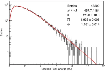
6.2.1 Polya Fit . . . 69
6.3 Calculation of the Number of Photoelectrons . . . 70
6.4 Time Resolution . . . 73
6.4.1 Signal Arrival Time . . . 73
6.4.2 SAT Uncertainty . . . 74
6.4.3 Slewing . . . 75
7 Modelling 77 7.1 Definition of the Model Components . . . 77
7.1.1 Photoelectron Drift Time . . . 78
7.1.2 Avalanche Propagation Time . . . 78
7.2 Mathematic Model . . . 81
7.2.1 Time Distribution . . . 81
7.2.2 Comparison of Different Drift Fields . . . 84
7.2.3 Avalanche Length . . . 85
7.2.4 Electron Multiplication . . . 88
7.2.5 Several Photoelectrons . . . 92
7.3 Summary . . . 93
8 Characterisation in a Laser Beam 97 8.1 Laser Setup . . . 97
8.1.1 Background Correction . . . 99
8.1.2 Photodiode Performance . . . 100
8.1.3 Attenuator Calibration . . . 101
8.2 Drift Distance . . . 105
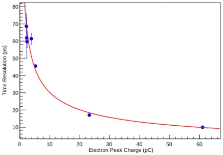
8.2.1 Time Resolution with Single Photoelectrons . . . 106
8.2.2 Summary . . . 108
8.3 Gas Types . . . 108
8.3.1 Waveforms of Neon-Ethane(-CF4) Mixtures . . . 109
8.3.2 Neon-CF4Mixture . . . 112
8.3.3 Time Resolution . . . 113
8.3.4 Time Resolution for several photoelectrons . . . 115
8.3.5 Gas Pressure . . . 117
8.3.6 Summary . . . 118
III Developments Towards a Particle Detector for High-rate
En-vironments
119
9 Characterisation in a Particle Beam 121 9.1 Beam Setup . . . 1229.1.1 Beam Telescope . . . 123
9.1.2 Trigger . . . 124
9.1.3 Triple-GEM tracker . . . 126
9.2 MCP-PMTs as a Time Reference . . . 130
9.2.1 Modeling of Cherenkov Light Propagation in the Radiator . . . 131
9.2.2 Characterisation with Beam Data . . . 134
9.2.3 Photek 240 PMT . . . 139
10 Time Resolution for MIPs 141 10.1 Woven mesh . . . 141
10.2 Thin-mesh . . . 142
10.3 Microbulk . . . 144
11 Resistive Read-out 149
11.1 Resistive Prototype . . . 149
11.2 Time Resolution in Muon Beam . . . 151
11.3 Operation in a Pion Beam . . . 152
11.3.1 Damage of the Photocathode . . . 153
11.4 Ion-Backflow . . . 154
11.4.1 Measurements of the IBF in the PICOSEC-Micromegas . . . 155
11.4.2 IBF in the Pion Beam . . . 156
11.5 Summary . . . 157
12 Segmented Read-out 159 12.1 Challenges of a Multipad detector . . . 159
12.2 Multipad Prototype . . . 162 12.3 Beam Characterisation . . . 163 12.3.1 Time performance . . . 163 12.3.2 Curvature . . . 165 12.4 Resistive Multipad . . . 168 12.5 Read-out Electronics . . . 168 12.6 Summary . . . 170 13 Photocathodes 173 13.1 Characterisation in a Particle Beam . . . 174
13.1.1 Metallic Photocathode . . . 174 13.1.2 Protected CsI . . . 175 13.1.3 Diamond-like Carbon . . . 175 13.1.4 Diamond nanoseeding . . . 176 13.2 Characterisation in a Monochromator . . . 178 13.2.1 ASSET-Chamber . . . 178
13.2.2 Boron Carbide Measurements in the ASSET Chamber . . . 183
13.3 Secondary Emission . . . 185
13.4 Electron Extraction at Different Electric Fields . . . 187
13.5 Summary . . . 188
Epilog
193
14 Conclusion and Discussion 193 14.1 Towards Implementation in a HEP Experiment . . . 19514.2 Future Applications of Fast-Timing Detectors . . . 196
14.2.1 Timing in Electromagnetic Calorimeters . . . 197
14.2.2 Time-of-flight Particle Identification . . . 197
15 Résumé en Français 201 15.1 Contexte Scientifique . . . 201 15.1.1 Micromegas . . . 201 15.2 PICOSEC-Micromegas . . . 203 15.2.1 Prototypes . . . 204 15.3 Caractérisation . . . 204 15.3.1 Modélisation . . . 204
15.3.2 Espace de Dérive et Mélange de Gaz . . . 205
15.4 Optimisation . . . 207 15.4.1 Multipad . . . 207 15.4.2 Résisitve Micromegas . . . 208 15.4.3 Photocathode . . . 209 15.5 Synthèse . . . 211
Appendix
215
A Appendix: Modelling 215 A.1 Input Parameters . . . 216A.2 Wald Distributions . . . 218
A.3 Field Scan . . . 222
A.4 Integration Length . . . 224
A.5 Avalanche Length . . . 226
A.6 Avalanche Multiplication . . . 228
B Appendix: Drift Distance Measurements 231 B.1 Time Resolution vs Number of Photoelectrons . . . 232
B.2 Time Resolution vs Drift Field . . . 233
B.3 Time Resolution vs Gain . . . 234
C Appendix: Gas Mixture Measurements 235 C.1 Time Resolution vs Amplitude . . . 236
C.2 Field Scan for Different Anode Settings . . . 238
Bibliography 243
List of Figures
2.1 MCP-PMT sketch . . . 7
2.2 Schematic cross-section of an LGAD pad . . . 11
2.3 Photograph of LGAD pads . . . 11
2.4 Schematics of an MRPC . . . 15
3.1 Bethe-Bloch function . . . 22
3.2 Electron interaction in matter . . . 23
3.3 Photon interaction in matter . . . 24
3.4 Argon escape peak . . . 25
3.5 Operation modes of gaseous ionisation chambers . . . 31
3.6 Sketch of an MWPC and an MSGC . . . 33
3.7 GEM electric field . . . 35
4.1 Micromegas sketch . . . 38
4.2 Microscopic picture of Micromegas meshes . . . 39
4.3 Bulk Micromegas production procedure . . . 41
4.4 Micromegas UV detection . . . 49
4.5 Micromegas time jitter . . . 51
5.1 Logo of the PICOSEC-Micromegas collaboration . . . 58
5.2 PICOSEC-Micromegas sketch . . . 60
5.3 PICOSEC sensor . . . 64
5.4 Technical sketches of the first prototype . . . 65
5.5 Picolarge readout sketch and pictures . . . 66
6.1 PICOSEC-Micromegas waveform . . . 68
6.2 Sketch of the DAQ setup . . . 68
6.3 Polya fit of the charge distribution . . . 70
6.4 Fit to determine the number of photoelectrons . . . 71
6.5 Procedure of extracting the number of photoelectrons . . . 72
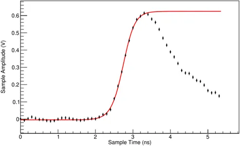
6.6 General sigmoid fit of the rising edge of a waveform . . . 74
6.7 Time resolution with slewing correction . . . 75
6.8 Slewing of the SAT and time resolution . . . 76
7.1 Schema of the avalanche propagation . . . 79
7.2 Wald distribution of the model for 350 V drift field . . . 83
7.4 Total time after the mesh modelled with different integration length . . . 86
7.5 Modelled signal time vs avalanche length . . . 87
7.6 Modelled signal time vs avalanche multiplication . . . 91
7.7 Comparison of all drift fields . . . 92
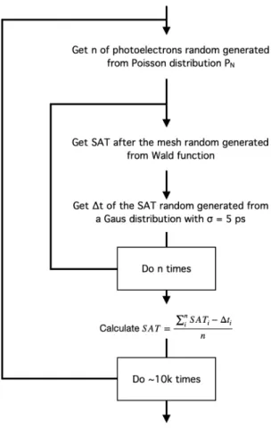
7.8 Block diagram of the toy Monte-Carlo . . . 94
7.9 MC modelling of many photoelectrons . . . 95
8.1 Sketch of the laser set-up . . . 98
8.2 Background correction of the noise . . . 100
8.3 PICOSEC-Micromegas and photodiode waveform . . . 101
8.4 Photodiode time resolutions . . . 101
8.5 Comparison of attenuator settings for single photoelectron conditions . . . 103
8.6 calibration of the laser attenuator . . . 104
8.7 Time resolution for different drift gaps . . . 106
8.8 Single p.e. time resolution vs electric field at different drift gaps . . . 107
8.9 Single p.e. time resolution vs gain at different drift gaps . . . 108
8.10 Drift velocity of COMPASS gas . . . 109
8.11 Mean waveforms at different gas mixtures . . . 111
8.12 Waveform without ethane . . . 112
8.13 Voltage settings for different gas types . . . 113
8.14 Time resolution for different gases and many photons . . . 116
8.15 Gain vs pressure . . . 118
9.1 Picture of the beam set-up cavern . . . 123
9.2 Sketch of the beam set-up . . . 124
9.3 Beam set-up picture . . . 125
9.4 Trigger set-up sketch . . . 126
9.5 NIM-module diagram for the trigger logic . . . 127
9.6 Triple-GEM voltage divider . . . 128
9.7 Cherenkov window sketch . . . 131
9.8 Geometrical calculation . . . 133
9.9 Charge density distribution of MCP-PMTs . . . 135
9.10 MCP-PMT time resolution in the inner 11 mm . . . 136
9.11 MCP-PMT ROIs . . . 137
9.12 MCP-PMT time resolution of different ROIs . . . 138
9.13 Spatial distribution of the time resolution . . . 139
9.14 Time resolution of the Photek 240 PMT . . . 140
10.1 Bulk mesh time resolution . . . 142
10.2 CsI quantum efficiency for the beam measurement . . . 143
10.3 Bulk mesh field scan . . . 143
10.4 Thin-mesh time resolution . . . 144
10.5 Modelling of a microbulk waveform . . . 145
10.7 Sigmoid fit of the microbulk waveform . . . 147
10.8 Microbulk time resolution . . . 148
11.1 Resistive prototype . . . 150
11.2 Sketch of the resistive Micromegas configuration . . . 151
11.3 Sketch of the floating strip readout . . . 151
11.4 Time resolution field scan of the resistive prototypes . . . 153
11.5 Ion exposed photocathode . . . 154
11.6 Sketch of the IBF with pre-amplification . . . 155
11.7 Ratio of current on the cathode . . . 156
12.1 Multipad readout PCB . . . 162
12.2 Multipad picture . . . 163
12.3 Mapping of the single pads on the segmented anode . . . 164
12.4 Multipad time resolution of a single pad . . . 165
12.5 Signal amplitude distribution for all pads . . . 166
12.6 Analysis ROIs of the multipad . . . 167
12.7 Multipad readout picture . . . 169
12.8 Photograph of the ATHR amplifier . . . 169
12.9 Comparison of the time resolution for different amplifiers . . . 170
13.1 2.5 nm DLC performance . . . 177
13.2 5 nm diamond nanoseeding . . . 178
13.3 Deuterium lamp spectrum . . . 179
13.4 Photograph of the ASSET set-up . . . 180
13.5 Sketch of the transmissive ASSET measurement set-up . . . 180
13.6 Photograph of the extraction mesh . . . 181
13.7 Sketch of the reflective ASSET measurement set-up . . . 182
13.8 Sketch of the ASSET radiation set-up . . . 183
13.9 Transparency of the B4C samples . . . 185
13.10B4C measurements in the Asset set-up . . . 185
13.11Photograph of a secondary emitter . . . 186
13.12Extracted photoelectrons at different drift voltages . . . 188
14.1 TOF particle identification . . . 198
14.2 PID-TOF momentum vs length . . . 199
15.1 La gigue temporelle des Micromegas . . . 202
15.2 Schéma du PICOSEC-Micromegas . . . 203
15.3 Signal modélisé en fonction de la longueur de l’avalanche . . . 205
15.4 Résolution temporelle en fonction du champ électrique à différents écarts de dérive 206 15.5 Image Multipad . . . 208
15.6 Photocathode exposée aux ions . . . 209
A.1 Wald distribution for 325 V drift . . . 218
A.2 Wald distribution for 350 V drift . . . 219
A.3 Wald distribution for 375 V drift . . . 220
A.4 Wald distribution for 400 V drift . . . 221
A.5 Field scan of the photoelectron time . . . 222
A.6 Field scan of the avalanche time . . . 222
A.7 Field scan of the total time before the mesh . . . 223
A.8 Field scan of the total time after the mesh . . . 223
A.9 Photoelectron time modelled with different integration length . . . 224
A.10 Avalanche time modelled with different integration length . . . 224
A.11 Total time before the mesh modelled with different integration length . . . 225
A.12 Total time after the mesh modelled with different integration length . . . 225
A.13 Modelled signal time vs avalanche length for 325 V drift . . . 226
A.14 Modelled signal time vs avalanche length for 350 V drift . . . 226
A.15 Modelled signal time vs avalanche length for 375 V drift . . . 227
A.16 Modelled signal time vs avalanche length for 400 V drift . . . 227
A.17 Modelled signal time vs avalanche multiplication for 325 V drift . . . 228
A.18 Modelled signal time vs avalanche multiplication for 350 V drift . . . 228
A.19 Modelled signal time vs avalanche multiplication for 375 V drift . . . 229
A.20 Modelled signal time vs avalanche multiplication for 400 V drift . . . 229
B.1 Multi p.e. time resolution for different drift gaps . . . 232
B.2 Time resolution for different drift fields and distances . . . 233
B.3 Time resolution for different detector gain and distances . . . 234
C.1 Time resolution for different gases and many photons . . . 236
C.2 Time resolution for different gases and some photons . . . 237
C.3 Field scan for different gas mixtures at single p.e. conditions . . . 239
C.4 Field scan for different gas mixtures at many p.e. conditions . . . 240
List of Tables
2.1 Overview of fast-timing detector technologies . . . 16
3.1 W-value for common gases . . . 21
4.1 COMPASS Micromegas ionisation length estimation . . . 52
5.1 Overview of the test chambers . . . 63
7.1 Comparison of model prediction and GARFIELD++ results . . . 84
8.1 1 p.e. time resolution of different gas mixtures . . . 114
8.2 Many p.e. time resolution of different gas mixtures . . . 115
10.1 Time resolution for different mesh technologies . . . 148
11.1 Comparison of different resistive anode technologies . . . 152
11.2 Ion backflow measurements . . . 157
12.1 Time resolution of different Pads . . . 166
12.2 Mean SAT on different Pads . . . 167
13.1 Metallic photocathodes . . . 175
13.2 Protected CsI . . . 175
13.3 Performance of DLC photocathodes . . . 177
15.1 Résolution temporelle de différents mélanges de gaz . . . 206
15.2 Performances des photocathodes DLC . . . 210
A.1 Model input parameters . . . 216
A.2 Model input parameter values . . . 217
List of Physical Constants
The physical constants and their approximated values used in this manuscript.
Physical Constant Symbol Value Unit
Archimedes’ constant π 3.1415
Avogadro constant NA 6,022 · 1023 mol-1
Electron charge e -1.6 · 10-19 C
Electron radius re 2.82 · 10-15 m
Electron rest mass me 0.511 MeV c-2
Fine-structure constant α 137-1
Muon rest mass mµ 105.66 MeV c-2
Planck constant h 6.626 · 10-34 J s
List of Abbreviations
ADC Analog-to-Digital ConverterALICE A Large Ion Collider Experiment APD Avalanche Photodiode
ASIC Application-Specific Integrated Circuit ATLAS A Toroidal LHC ApparatuS
AUTh Aristotle University of Thessaloniki BBO Barium-Borate
CAD Computer-Aided Design CAST CERN Axion Solar Telescope CCD Charge Collection Distance CCE Charge Collection Efficiency CCQE Charged Current Quasi-Elastic CEA Commissariat à l’énergie atomique CENF CERN Neutrino Facility
CERN Conseil Européen pour la Recherche Nucléaire CFD Constand Fraction Discrimination
CMS Compact Muon Solenoid
COMPASS Common Muon and Proton Apparatus for Structure and Spectroscopy CVD Chemical Vaporised Diamond
DAQ Data Acquisition
DEDIP Département d’Électronique des Détecteurs et d’Informatique pour la Physique DIRC Detection of Internally Reflected Cherenkov Light
DLC Diamond-Like Carbon
DNCD Boron-Doped Nanocrystalline Diamond DUT Detector Under Test
EIC Electron-Ion Collider
EMC Electromagnetic Calorimeter
ENUBET Enhanced NeUtrino BEams from kaon Tagging ESS European Spallation Source
FEC Front-End Card
FWHM Full Width at Half Maximum GDD Gaseous Detector Development GEM Gas Electron Multiplier
GIF++ Gamma Irradiation Facility
HDMI High-Definition Multimedia Interface HEP High Energy Physics
HFS Hyper-Fast Silicone
HL-LHC High Luminosity-Large Hadron Collider HV High Voltage
IBF Ion-Backflow
ILC International Linear Collider IR Infrared
IRFU Institut de Recherche sur les lois Fondamentales de l’Univers LCD Laboratoire Capteurs Diamant
LED Light-Emitting Diode
LEP Large Electron-Positron Collider LGAD Low Gain Avalanche Detector LHC Large Hadron Collider
LIDYL Laboratoire Interactions, Dynamiques et Lasers
LIST Laboratoire d’intégration des systèmes et des technologies MAMMA Muon ATLAS MicroMegas Activity
MCA Multichannel Analyser
MCP–PMT Microchannel Plate – Photomultiplier Tube Micromegas MICRO-MEsh GASeous detectors MINOS Magical Numbers Of Shell
MIP Minimum Ionising Particle
MPGD Micro Pattern Gaseous Detector MRPC Multi-gap Resistive Plate Chamber MSGC MicroStrip Gas Chambers
MWPC Multi-Wire Proportional Chamber nBLM neutron Beam Loss Monitor NEA Negative Electron Affinity NIM Nuclear Instrumentation Module NSW New Small Weel
nTOF neutron Time-Of-Flight Facility p.e. Photoelectron
PCB Printed Circuit Board
PDF Probability Density Function PET Positron Emission Tomography PID Particle Identification
PMT Photomultiplier Tube
PTC Programmes Transversaux de Compétences QE Quantum Efficiency
R&D Research and Development
RADIAMM Radiation hard Diamond-based secondary emitter for delevopment of an ultra fast
timing MicroMegas detector
RMS Root Mean Square ROI Region Of Interest RP Roman Pot
RPC Resistive Plate Chamber S/N Signal-to-Noise Ratio SAT Signal Arrival Time
scCVD Single Crystalline Chemical Vaporised Diamond SEDI Service d’Electronique, des Détecteurs et d’Informatique SHG Second-Harmonic Generation
SiPM Silicon Photomultiplier SMA SubMiniature version A SMC SubMiniature version C
SPAD Single-Photon Avalanche Diodes SPS Super Positron Synchrotron SRS Scalable Readout System sTGC strip Thin Gap Chamber T2K Tokai to Kamioka
TMAE Tetrakis(dimethylamine)ethylene TOF Time-of-Flight
TOP Time-of-Propagation TOT Time-over-Threshold TPC Time Projection Chamber
USTC University of Science and Technology of China UV UltraViolet
VPTT Vacuum Phototetrodes
Everything starts from a dot
1 Motivation
S
ince the dawn of time humankind yearns for the understanding of what was, is, and will be. Various disciplines of academia are pursuing this quest. The subjects of humanities like Philosophy, Theology, and Psychology as well as the natural sciences like Biology, Chemistry and certainly Physics are sharing this virtuous hunt. All academic disciplines are driven by one fundamental question which can not be expressed more beautifully and accurately than by the words of the German writer Johann Wolfgang von Goethe. In his tragic play Faust the eponymous main character, a striving savant, is desperately seeking to answer his question of “so that I may perceive whatever holds, the world together in its inmost folds”[1].Physics and more precisely, particle physics is interpreting this question as to the longing to explore the smallest building blocks and its interactions that make up all the known and unknown universe. One theory that can at least partly describe the composition of known matter and its interplay in the universe is the Standard Model. It is based on an accumulation of theories about different families of particles and their forces. Nowadays, ever-increasing experiments are required to study the last unknown of the Standard Model and beyond. In the past, smaller laboratory experiments were sufficient to gain new knowledge of the fundamental forces and particles. One example for this smaller experiments is the measurement of the elementary electric charge by R. A. Millikan [2].
One of the biggest facility to study particle interactions and to move the remaining frontiers of human knowledge is the Conseil Européen pour la Recherche Nucléaire (CERN). It hosts the, up-to-now, largest and most powerful particle accelerator in the world. The Large Hadron Collider (LHC) has a circumference of 27 km and centre-of-mass collision energy of 13 TeV for proton-proton collisions. Each high energetic collision generates a vast amount of particles scattered in all directions and with different remaining momenta. The underlying physical process that generates these particles is reconstructed with accurate identification of the particles and their energy and direction. Theories of the physical processes in the Standard Model and beyond can be verified or discarded from the reconstruction of the collision products. Each detector component needs to fulfil specific precision requirements in spatial, time and energy resolution to provide the needed accuracy in reconstructing all necessary information of the particles.
The four big LHC experiments, the additional experiments at CERN, and countless other earth and space-bound experiments have already collected a sheer amount of data. All these exper-iments have contributed to our understanding of the world and its underlying physical processes. However, there are still open questions and processes not yet fully understood like the neutrino oscillation mechanism, dark matter, CP violation and many more. New experiments must be con-ceived and built to address these questions. An already planned LHC upgrade will raise its nominal luminosity (HL-LHC) to detect the footprint of even more rare physical processes and long-term
projects of future linear and circular colliders are being proposed. Those colliders will significantly raise the centre-of-mass collision energy to enable the study of countless new physical phenom-ena. Not only large scale experiments are planned to address the remaining questions in particle physics. Smaller, but very specialised, (astro)particle experiments are planed all over the world to detect very rare events to complete the puzzle from all sides.
These new experiments are demanding a new generation of particle detectors with ever-increasing accuracy. Not only the performance need to evolve, but even the robustness has to improve as the detectors need to withstand several years to decades in an environment with persis-tent radiation and a strong flux of particles. For the HL-LHC upgrade a time resolution of the inner tracking detectors of 20-30 ps is needed for an accurate vertex separation, while the luminosity is expected to increase towards ∼5-10 x 1034cm-2s-1 [3]. This first estimation directs the devel-opment of future tracking systems towards a regime of radiation hard detectors with few tens of picosecond time resolution that reduce the pileup and improves the vertex separation of different particles. Fast-timing detectors can be moreover useful for other sub-systems of particle physics experiments. The background rejection efficiency in calorimeters and the maximal momentum for time-of-flight particle identification can be improved.
The PICOSEC-Micromegas detection concept is one possible answer to the demands of de-tector systems in future particle physics experiments. It is the first Micro-Pattern Gaseous Dede-tector (MPGD) that reaches a time resolution in the required range for future fast-timing detectors [4, 5]. This manuscript gives a detailed description of the PICOSEC-Micromegas concept. It explains the detection principle and describes the tested prototypes. An extensive series of characterisation measurements have been carried out to understand the impact of each detector component on de-tector timing and robustness. The bouquet of characterisation methods ranges from Monte-Carlo simulation over precision measurements with a laser facility up to large scale measurements in a particle beam. Based on this characterisations, new detector modules are presented and tested that lead the PICOSEC-Micromegas concept towards a versatile tracking detector for high-rate environments.
All in all, a comprehensive view of this new detector technology is given. Moreover, its possible applications in future particle physics experiments are elaborated. This work shows the different steps required in the development of a new cutting edge detector technology. In future physics experiments, PICOSEC-Micromegas might help humankind to understand piece by piece “whatever holds, the world together in its inmost folds”.
2 State-of-the-Art Fast-timing
Detectors
Contents
2.1 Introduction to Fast-Timing Detectors . . . 5 2.2 MCP-PMT . . . 6 2.3 Photodiodes . . . 8 2.3.1 APDs . . . 9 2.3.2 SiPMs . . . 9 2.3.3 LGAD . . . 11 2.4 Wide-gap Semiconductors. . . 12 2.5 Resistive Plate Chambers . . . 14 2.6 Summary of Fast-Timing Detector Technologies . . . 15
I
n the following, a brief overview of the different current state-of-the-art detectors suitable for fast-timing applications is given. This chapter begins with an introduction into the virtue of fast-timing detectors, explaining the main parameters limiting the timing performance of a detector. At the end of this section, a table summarises the discussed technologies, applications, and typical time resolutions. This detector overview and its current applications are not exhaustive as the fast-timing detector development is rapidly growing, but it will help to sort the develop-ment and results of the PICOSEC-Micromegas into a broader context. MicroPattern Gaseous Detectors (MPGDs) for fast timing applications are not discussed in this section as the PICOSEC-Micromegas concept is currently the only successful development of MPGD as a fast-timing de-tector.2.1 Introduction to Fast-Timing Detectors
R
eal detectors will always have limited accuracy when detecting particle energy, position and timepoint. These limited accuracies are manifested in jitter of the signal charge; the charge spread on the read-out anodes; and jitter in the signal arrival time (SAT). These three characteristic properties are affected by different components of a detector and can be im-proved individually in the development process of a detector. Anyhow, the improvement of one property can also affect another, like the improvement of spatial resolution with an improved timeresolution. This work focuses mainly on the time resolution and thus the reduction of the SAT jitter, which is an interplay of many physical effects taking place in the detector and the read-out electronics. The rising edge of a signal determines the SAT, and the main distortion to the rising edge is added by electronic noise. Hence, a first-order approximation of the detector time reso-lution (σtot) is calculated by the signal rise time (trise) divided by the signal-to-noise ration (S/N ) as
σtot ≈ trise
S/N . (2.1)
This approximation is commonly used in the domain of communication engineering as a rule of thumb. For example, the PICOSEC-Micromegas has a rise time of ∼1 ns and needs, therefore, a signal-to-noise ratio of ∼50 to reach a time resolution in the order of ∼20 ps.
Different components contribute to the total time resolution in a detector set-up separately and the total time resolution is defined by the sum of the variances for each of these contributions. The total time resolution can be expressed on a macroscopic level as
σ2tot= σ2elec.+ σTTS pNp.e.
!2
+ σt02 + σ2track+ ... , (2.2)
where σelec. is the electronic noise of the signal, σTTS/pNp.e. is the single-electron transit time spread divided by the number of photoelectrons in a photodetector, σt0is the time resolution of the trigger system in a measurement set-up, and σtrackis the contribution of tracking effects depending on the track geometry [3]. Depending on the composition and the actual application of the de-tector, not all of these components contribute significantly to the time resolution, and even other components may become important. For the study of the PICOSEC-Micromegas detector, we will see that the main parameters are the electronic noise, the transit time spread and the number of photoelectrons.
2.2 MCP-PMT
T
he first presented fast-timing detection concept is the Microchannel Plate - Photomultiplier Tube (MCP-PMT). It is a derivation of classical PMTs with an advanced time response. In a classical PMT an inevitable time jitter is caused by different path lengths of the electrons between the dynode amplification stages. In the MCP-PMT technology, thick ceramic plates with several micro holes are substituting those dynodes. The microchannels plates are placed into a vacuum tube, and an intense electric field is created inside of the microchannels with metallic electrodes on both sides of the plates.A photocathode in front of the microchannel plates emits electrons. The electric field in-side the microchannels accelerates those electrons, which extract more electrons when interacting at sufficient energy with the microchannel walls. Figure 2.1 shows a sketch of the electron am-plification inside one microchannel. With ∼10 µm diameter, the travel distance of the electrons from one wall to the other is significantly smaller compared to the distance between the dynodes
of several centimetre in a classical PMT. This shorter drift distance reduces the time jitter. Several microchannel plates can be stacked over each other inside of one vacuum tube for a multi-stage amplification [6, p. 188].
Figure 2.1: Left: Single microchannel plate. Right: Electrons are amplified in each microchannel when interacting along the channel walls. Image extracted from reference [6, p. 188]. MCP-PMTs are one of the available detector technologies with the best time resolution. However, they are not suitable to cover large detection areas due to its production cost. They are not suitable as vertex detector in a LHC experiment (i.e., near the interaction point) due to its larger amount of material compared to other technologies and more critical the rather low robustness of the photocathodes [7]. MCP-PMTs are used for applications where a small active area is sufficient like, for example, for beam monitoring devices of the European spallation source (ESS) proton beam. This application favours MCP-PMTs more for their gain characteristics than for the time performance [8]. MCP-PMTs are additionally used as a time reference detector for the PICOSEC-Micromegas beam measurements. Section 9.2 in this manuscript gives a characterisation of two MCP-PMTs with a combined time resolution measured as low as 7.2 ± 0.1 ps [9].
Large particle physics experiments use MCP-PMTs for particle identification detectors (P-IDs) detecting the internally reflected Cherenkov light (DIRC). One example is the Belle-II time of propagation (TOP) detector, which is a ring imaging Cherenkov detector placed as a barrel between the tracking detector and the calorimeters. It consists of long quartz radiators that are read out at one end by small MCP-PMTs. It is used for particle identification (PID) and is especially effective in the discrimination between pions (m0(π±) = 139.57 MeV/c2) and kaons (m0(K±) = 439.68 MeV/c2), because the Cherenkov cone opening angle variates for these particles due to their different momentum at the same energy. The light radiated at different Cherenkov angles propagates in different paths through the radiator and reaches the MCP-PMTs on different areas and at different times. A fast-timing detector like MCP-PMTs is a sensitive detector for these small propagation differences [10]. Belle-II MCP-PMTs are reaching a time resolution as low as 6.2 ps for time of flight measurements of 3 GeV/c pions [11].
2.3 Photodiodes
S
emiconductor photodiodes with a band-gap between the conduction and the valence band of 1-1.5 eV are the second presented technology. The most prominent semiconductor in this range is Silicon with a band-gap of 1.12 eV at room temperature [12], but there are many others used in particle detectors like germanium or compounds like GaAs or InGaAs. One of the first use of semiconductors in HEP was as a precise tracking detector in the late 1970s [13].Photodiodes are built up of several differently doped layers of semiconductors. One layer consists of a silicon crystal lattice, and each layer can be doped by adding different other elements to the lattice. A surplus of electrons is generated in the valence band when phosphor is added to the lattice. Those layers are called n-doped and phosphor acts as an electron donor. Aluminium can be added on the contrary to phosphor to generate electron holes in the valence band. In this way, added aluminium forms p-layers as an electron acceptor. The ratio of doping material to silicone can be variated to generate n- and p-layers with different intensity. A + or - can be used as indices to symbolise layers with different doping ratio. It is also possible to build photodiodes on other semiconductor bases instead of silicone (like GaAs or InGaAs photodiodes). The choice of doping material changes in this case, according to the different substrate material.
A typical photodiode is constructed with an intrinsic layer without any donation between a pn-junction (p+− i − n+). It is used as a spatial boundary between the different doped layers, and it absorbs photons. Photons reaching the intrinsic layer with sufficient energy generate electron-hole pairs by the extrinsic photoelectric effect.
Photodiodes can be operated in three different modes depending on the bias voltage applied. Without additional voltage, a photodiode operates in zero biased mode. The generated photoelec-trons create an electric field in the diode until the photocurrent can overcome the impedance of the electric circuit. This mode is mainly used for photovoltaic cells as the electric current is efficiently drained from the photodiode.
The second mode is the photoconductive mode. The photodiode is reverse biased with a negative voltage applied to the p+-layer on the anode. The intrinsic zone gets widen by the bias voltage and a stronger electric field forms between the cathode and the anode. The electrical po-tential of the diode rises with the additional electrons created in the intrinsic zone. This mode is commonly used to measure light intensities, as the current flowing from the diode is linear correlated with the initial photon energy. The electric field and the reduced capacity due to the bi-ased voltage improve the detector time resolution [14]. A photodiode operated in photoconductive mode is used as a t0reference and trigger detector in the laser set-up described in section 8.1. The laser provides enought light to generate large signals in the photodiode leading to adequate time resolution as a reference detector.
The third mode is the avalanche photodiode (APD) mode, with even increased reverse bias voltage. It provides the best time resolution with the highest gain, and different silicon detector technologies in HEP are based on APDs.
2.3.1 APDs
A
PDs are operated with a reverse bias higher than the breakdown voltage, which creates astrong electric field that accelerates the free-moving electrons. They have moreover a slightly different structure than classical PIN-diodes with the following layer structure: p+− i − p − n+. More free electrons are formed by interactions of the electrons in the transition zone between the p and the n+layer. This zone is referred to as multiplication zone. The free-moving electrons will form an electron avalanche in the diode, and the diode will be conducive for a short time.A resistor quenches the occurring current after the anode. In this way, the photodiode is a digital counter which gives a uniform signal every time photons hitting the active area. These signals do not contain any energy information, but even single photons can be precisely detected. This operation mode of a photodiode is called Geiger mode, as it behaves like a Geiger-counter. The electron avalanches can propagate faster than the free moving electrons through the diode, which results in a time resolution of 20 ps (FWHM) [15].
Large area APDs are used in the antiproton annihilation experiment Panda in Darmstadt in the forward endcap of the electromagnetic calorimeter (EMC). The APDs have an active area of 14 x 6.8 mm2and two APDs are used to read out one square PbWO-II scintillator crystal. The Panda experiment hosts a magnetic solenoid that generates a magnetic field of up to 2 T at the EMC. APDs are preferred over conventional PMTs for its operation independent of magnetic fields. They are moreover selected for the EMC due to its quantum efficiency and gain charac-teristics. An operation in a cooled down environment of T = −25◦C additionally increases the gain of the APDs. The particle flux and expected radiation damage in the inner parts of the endcap EMC are too high for a long term operation of APDs. Vacuum phototetrodes (VPTTs), a small PMT derivation, are developed for this region with inferior detection performance but increased durability under higher particle flux [16].
One of the most widespread detectors is silicon photomultiplier (SiPM), which has found an excellent reputation outside of HEP in medical imaging applications. The use of fast timing silicon detectors in future HEP experiments is challenging, as semiconductor-based devices are by default not very radiation hard. A highly energetic or heavy particle can create defects in the semiconductor lattice, which leads to space charge effects or even leakage current. One of the most promising developments of more radiation hard fast-timing silicon detectors are the low gain avalanche detectors (LGAD). An overview of the SiPM and LGAD detection concepts are given in the following.
2.3.2 SiPMs
M
ultiple APDs can be parallel interconnected to form a SiPM. Each of the APD microcellshas a size of a few µm whereas SiPM sensors can reach up to several mm and contain hundreds of APDs. The SiPM signal is a superposition of all APD signals, and the amplitude is correlated with the number of activated APDs in one SiPM sensor. SiPMs are therefore suitable for calorimetry measurements as information on the amount of light is extracted from the signal, and the fast-timing properties of the APDs are preserved [17].The overall performance of silicon detectors strongly depends on the surrounding temper-ature. A higher gain can be achieved at lower temperatures. For test measurements and operation the usual target temperature lies between −25◦C and −20◦C. A higher detector gain improves the signal-to-noise ratio and thus the time resolution of any detector. The time resolution of SiPMs has been measured to 35 ps in a proton beam with a Cherenkov radiator in the front and ∼15 photo-electrons [18], while the time resolution for single photoelectron ranges between 176 ps and 330 ps (FWHM). An advanced type of SiPM based on single-photon avalanche diodes (SPADs) instead of APDs is further developed. These are quenched microcells that need only one photon to generate an avalanche. The time jitter contribution of a SPAD to a SiPM signal in a single photoelectron measurement is estimated to ∼20 ps (FWHM) after subtraction of the electronic noise [19].
SiPMs are in a rather mature development stage compared to the other presented fast-timing detector technologies and are used in various applications in physics and industry. However, they are likely to suffer from radiation damage. Therefore, they are mainly placed in outer parts of a HEP experiment. SiPMs are very suitable to read out calorimeter scintillators as their quantum efficiency is an advantage, and the timing information can be further used for particle discrimina-tion.
SiPMs are considered as one option for the calorimeter upgrades of the HL-LHC detectors and other HEP experiments in design phase, like the international linear collider (ILC). The ILC is planned to be constructed in Japan, and it will be the first large-scale linear e+-e-collider with a centre of mass energy of 200 - 500 GeV in the first expansion stage [20].
A primary application domain of SiPMs lies outside of fundamental research. Medical imaging in the positron emission tomography (PET) is widely using SiPMs. This is a medical imaging procedure where a β+radiating substance is injected in a living organism. This substance accumulates in parts of the body with cancer cells. The β+decay radiates positrons, which annihi-late with surrounding electrons and two photons with an energy of 511 keV each are then radiated diametrical. Those photons can be detected outside of the body, and the origin of the annihilation can be extrapolated from the photon detection positions. The time of flight (TOF) of these photons is additionally measured for background reduction. Advanced PET scanner usually consists of circular aligned fast scintillators like doped CsI or L(Y)SO to detect the annihilation photons and SiPMs to detect the scintillator light. The short decay time of the scintillator and the fast time re-sponse of the SiPM improves the spatial and TOF accuracy [21]. Industrial available PET scanners are reaching a TOF time resolution of 210 ps (FWHM) [22].
SiPMs can only detect photons directly. They need an additional photon converter like a scintillator to detect massive particles as required in HEP experiments. Another semiconductor fast-timing detector suitable to measure particles directly like MIPs is the Low Gain Avalanche Detector (LGAD) presented in the following.
2.3.3 LGAD
L
GADs are a rather newly developed detector concept driven by the needs of HL-LHC exper-iments, with the aim to develop fast and small APDs withstanding the prospected particle fluences after the upgrade.LGADs have a similar structure to APDs except for the intrinsic layer, which is replaced by a positive doped p-layer next to a highly negative doped n+-layer. Figure 2.2 shows a schematic cross-section of the differently doped layers from one LGAD pad. The high charge gradient be-tween the n+/p junction creates a strong electric field, where electrons from the n+ cathode are directly multiplied. This configuration reaches a gain of up to 10. The purity of the doping and the uniformity of the electric field defines the gain and operation stability. A specific junction termi-nation extension consisting of n-doped walls helps to make the electric field uniform until the end of the detector [23].
Figure 2.2: Schematic cross section of an LGAD with a p-layer directly under the n+ cathode and n-doped junction termination extensions (JTE) on the sides. Image extracted from refer-ence [23].
Figure 2.3: Photograph of three
LGAD detector pads for the CMS upgrade on a testboard. Each pad is 1 x 1 mm2 large and contains 9 cells with a size of 50 x 50 µm2. First radiation studies of LGADs have shown a lower gain after radiation exposure. Mea-surements have been conducted with samples before and after radiation of neutron, protons and hadrons up to an 1 MeV neutron equivalent fluence of Φeq. = 1016cm-2. Mainly the charge collec-tion efficiency degrades over time in a high-flux environment as more and more boron is removed from the p-layer. The degeneration of the p-layer diminishes the amplification field between the n+/p junction and thus reduces the signal multiplication. The lower gain moderates the linear in-crease of the leakage current at increasing generation current under high fluence. A higher electric field can be applied to the detector after irradiation to recover (partly) from the gain loss. This procedure allows the operation of LGADs at higher fluence compared to p − i − n diodes [24].
The first generation of LGAD detectors with a thickness of 300 µm were tested in a 170 GeV pion beam at CERN and a time resolution as low as 120 ps was reached and 65 ps was measured in an IR Laser set-up [25]. The time resolution in the Laser measurement is significantly
better as only the intrinsic time jitter of the detector is contributing to the time resolution. The energy transfer from the particle to the semiconductor follows a Landau fluctuation, while the time walk due to this fluctuation has to be included for beam measurements. Furthermore, the time resolution depends on the detector capacitance and the general detector noise [25]. Thinner LGADs with a lower capacity have been developed. Prototypes with a thickness of 45 µm are tested in a particle beam before and after irradiation. Figure 2.3 shows a photograph of an LGAD test board for the CMS experiment. The tested LGAD chips are 1 mm square containing nine cells of 50 µm square, which corresponds to a filling factor of 2.25 %. Before irradiation a time resolution of less than 30 ps has been reached at −20◦C at the maximum stable voltage. An increase of the surrounding temperature to −6◦C shows degeneration of the time resolution of 8 ps at the same voltage. This behaviour is expected due to the lower impact ionisation coefficient at higher operation temperature and thus lower gain. After irradiation with Φeq. = 1015cm-2 the gain-loss could not be fully compensated by a higher bias voltage and a best time resolution of 57 ps was measured [26].
The CMS collaboration chooses LGADs as a high granularity timing detector for the high luminosity upgrade. The actual CMS calorimeter will not provide sufficient precision to recon-struct the vertices of low energetic MIPs in the HL-LHC phase. This limitation will be eliminated by an extra detection layer of precise timing detectors to the barrel and endcap structures. The barrel will be equipped with SiPMs and LYSO:Ce scintillators, as the radiation is expected to be maximum 25 kGy with a particle flux of 2·1014cm-2(1 MeV neq) at η = 1.45. The SiPM-LYSO:Ce combination reaches a time resolution of 21 ps (σ) with MIPs and a pixel size of 6 x 6 mm2 on a 3 mm thick crystal. The endcaps (1.6 <|η| <3.0) will face a magnitude higher particle flux with 1.7 · 1015cm-2 (1 MeV neq) corresponding to 690 kGy at an integrated luminosity of 4000 fb-1. LGADs are one option for the endcaps to reach a time resolution in the order of 30 ps with suffi-cient robustness [27]. A similar detector concept is proposed and studied for the ATLAS Phase-II upgrade [28].
2.4 Wide-gap Semiconductors
D
iamond, as carbon in a crystalline lattice, has a band-gap between the valence and the con-ductive band of 5.48 eV [12]. Such materials are placed between insulators and classical semiconductors and are called wide-gap semiconductors. Charged particles and photons passing through a diamond detector ionise atoms like in a silicon detector. The main difference to a standard semiconductor is the lack of an intrinsic layer between a p-n-junction. In a wide-gap semiconductor, the whole detector volume is sensible for electron-hole-pair creation. The number of initially generated electrons is linear to the deposed energy of the detected particle. Diamond detectors can be produced as thin detectors with an exceptional radiation hardness and high atom density. These kind of detectors are well suitable for radiation detection [29] and dose monitoring [30, 31] and are mostly used for beam monitoring and medical applications.Diamond detectors are moreover capable of providing an intrinsic time resolution better than 29 ps (σ) with a detector thickness of 100 µm [32]. Due to the higher band-gap, a higher electric field can be applied to the diamond without reaching the breakdown voltage. The electric
field moves the ionised electrons in the conductive band along the diamond lattice. The high electric field can bring the electrons to a higher thermal state than the lattice, and the electron can scatter between energy bands by transferring energy to the lattice. The possibility of electron scattering from higher energetic bands to lower ones depends on the field orientation related to the lattice structure. This effect leads to an anisotropy of the drift velocity, and the saturated carrier velocity of the electrons in strong electric fields is higher in diamonds than in silicon-like semiconductors.
The charge transportation in a semiconductor is sensitive to lattice defects causing recom-bination and charge trapping. As diamonds are wide-gap semiconductors, the direct recomrecom-bination between two bands is negligible. Trapping of electrons in lattice defects and trap induced recom-bination is instead a severe concern for diamond detectors. The impact of defects on the charge mobility is expressed with two values: the charge collection distance (CCD) and the charge collec-tion efficiency (CCE). The CCD gives the mean drift distance of a moving charge in the detector before it gets trapped, and it should be much higher than the detector thickness for an efficient detector. The second value, the CCE, is directly related to the CCD and the thickness, as it gives the fraction of collected charges to the generated charges. The trapping of space charges can cause irregularities in the detector behaviour. When many charges are generated in a small area, e.g. due to an α-particle, lattice defects can be all filled in that area by fixed space charges, polarising it. This polarised area generates an own field in the detector, deteriorating the pulse height. A second effect is the priming when defects are filled regionally over a longer distance, and the CCD can improve in that area. The regional defects cause an inhomogeneous behaviour of the detector.
Reproducible and regular diamond lattices with few defects are required for stable operating fast-timing detectors. These diamond lattices can be artificially produced with the single crystalline chemical vaporised diamond (scCVD) method. In this method, carbon atoms are vaporised to a gas state, and a clean substrate surface is coated with these diamonds. As carbon cannot be evaporated as a pure element, it is done as part of a precursor molecule. A typical precursor gas for CVD production is methane (CH4). The methane is highly diluted with hydrogen (1-1.5 % vol. methane) and the gas mixture is heated above 700◦C. The hydrogen reacts with the methane and reactive methylium cations (CH+3 are formed. Under the right pressure and temperature, the cations can react on a substrate surface, and carbons can form a single crystalline diamond lattice [33].
One application of scCVDs with a need for fast-timing properties is the detector upgrade of the Totem experiment at CERN. The Totem detector is placed at the same interaction point of the LHC as the CMS experiment. It is designed to study elastic and diffractive scattering with a focus on precision measurements of the total cross-section of proton-proton scattering. The core detectors of Totem are two, so-called, roman pots (RPs) at each side of the interaction point. These are vacuum vessels (pots) containing precise tracking detectors to detect the scattered particles under a low angle close to the interaction point. The first version of the RPs has used silicon strip detectors [34].
The increasing luminosity of the LHC demands a more robust solution as a tracking de-tector close to the beamline. The additional capability of TOF measurements with fast-timing detectors allows the vertex reconstruction in the z-direction and matching with the CMS tracker data. ScCVDs are fulfilling all RP upgrade criteria, as they provide proper tracking and timing
capability on a small size detector with improved radiation hardness compared to silicon detectors. Measurements with two complete scCVD detector units have shown a time resolution per strip of down to 80 ps, which is below the required design performance of 100 ps [35].
2.5 Resistive Plate Chambers
T
he last presented detector type for fast-timing applications is the resistive plate chamber (RPC) and recent development called multi-gap resistive plate chamber (MRPC). RPCs are gaseous ionisation detectors with two parallel plates as electrodes. The plates have a typical distance of some millimetres, and a uniform electric field of ∼1KV/cm is created between the plates. Particles ionise the gas atoms, typically a noble gas like argon, and free-moving electrons are created. Electrons are then accelerated along the electric field towards the anode plate and can create further electrons in an avalanche. The electrode plates are coated with bulk resistive material, e.g. bakelite, so that a discharge of the gas due to the ionisation is spatial limited, and the surrounding sensitivity stays unaffected. The moving electrons induce an electric signal in the electrode plates while drifting towards the resistive coating.Because of the high resistivity, RPCs can be operated under high particle flux. Large area detectors are built as the cost and material budged is rather low compared to scintillators, and a strip segmentation of the read-out plane preserves the spatial information of the passing particle. A time resolution of the order of nanoseconds can be reached [36].
MRPCs are a recent development of RPCs for a better timing performance. Several electri-cally floating resistive plates placed in a larger drift gap between the electrode plates that generates a strong electric field. The segmentation of the volume limits the spatial distribution of ionisations inside one gaseous volume and the drift distance of the generated electron. The signal for each de-tected particle is fully induced in the electrodes when the electrons are reaching the next resistive plate. They do not need to travel the whole distance until the anode plate, which improves the time resolution of the detector to sub nanoseconds [37].
Figure 2.4 shows the schematic of an MRPC with four independent electric fields and each of them separated in six gaps by additional floating resistive plates (light green). The differential signals from the anode and cathode are read out and processed by dedicated front-end electronic. One particle can create several signals in the detector, and the flight path can be reconstructed by the position and the time of each signal. The construction scheme of the MRPC reaching the best time resolutions is shown in figure 2.4. The distance between each resistive plate is 160 µm for this detector and it was operated with a gas mixture of C2F4H2 (95 %) - SF6 (5 %). A time resolution with two of these chambers in a 5 GeV/c secondary particle beam has been measured to 30/√2 = 21.2 ps (σ). A further increase of the time resolution is limited by the front-end electronics, and the signal propagation along the 2.45 x 7.4 cm2read-out strips [38].
One application of MRPCs in HEP is the TOF upgrade of the ALICE detector at CERN. Time of flight measurement is used to identify charged particles. A time resolution of less than 100 ps is required for a 3σ separation between π/K in the momentum range of 0.5-2.5 GeV/c. MRPCs are chosen to cover a large area with detector elements of 120 cm length in an environment
Figure 2.4: Schematic sketch of an MRPC with 24 gaps (160 µm each) in four separate electric fields. Image extracted from reference [38].
with particle fluxes of 50 Hz/cm2from Pb-Pb collisions. Detectors with two stacks of electric fields and five gaps in each field are used. The gap distance is 250 µm and a time resolution of 48 ps after slewing correction has been measured [39].
2.6 Summary of Fast-Timing Detector Technologies
A
n overview of the state-of-are of fast-timing detectors is made in table 2.1. The presented detector technologies have advantages and disadvantages, which makes them suitable for different applications. Some of the presented technologies are not only used for fast-timing applications. The PICOSEC-Micromegas, results presented in this manuscript, will be compared to the existing technologies, and it will show its own advantages defining new applica-tion modes. In general, a direct comparison of the measured values is difficult as the detectors are tested in different conditions and the time resolution is extracted in different ways. A comparison of the maximum particle rate is not possible, as these data are not available for all detector types.Table 2.1: Overview of fast-timing detector technologies. The typical field of application and the achievable time resolution of the technologies are listed. Some entries have a short comment underlining its (dis)advantage or giving further information of the time reso-lution.
Detector Type Application Project σ (ps) Ref.
MCP-PMT TOP PID BELLE-II 6.2 [10, 11]
MCP-PMT t0-reference PICOSEC-Micromegas <7.2 [9]
combined resolution of two MCP-PMTs PIN Photodiode t0-reference PICOSEC-Micromegas <4.7
upper limit for laser tests
APD EMC Panda ∼8.51 [15, 16]
not radiation hard, but unaffected by magnetic fields
SiPM R&D ILC 35 [18]
SiPM Calorimeter CMS 21 [27]
SiPM PET TOF Medical Imaging ∼902 [22]
small size
LGAD Calorimeter Atlas, CMS 57 [26, 27, 28]
better radiation hardness compared to SiPMs
scCVD R&D 29 [32]
scCVD Tracker TOTEM (RP) 80 [35]
radiation hard and small sized
MRPC R&D 21.2 [38]
MRPC TOF PID ALICE 48 [39]
large area coverage
PICOSEC R&D 24 [5]
120 ps (FWHM) 2210 ps (FWHM)
Poca favilla gran fiamma seconda;
— Dante Alighieri (1265-1321), Divina
Commedia: Paradiso I (1320)
“A little spark is followed by great flame”, Dante Alighieri (1265-1321), Divine Com-edy: Paradise I (1320)
3 Working Principle of Gaseous
Detectors
Contents
3.1 Gas Ionisation . . . 20 3.1.1 Charged Heavy Particles. . . 21 3.1.2 Electrons . . . 22 3.1.3 Photons. . . 23 3.1.4 Heavy Neutral Particles . . . 26 3.2 Electron Transport and Amplification in the Gas . . . 27 3.2.1 Drift . . . 27 3.2.2 Diffusion . . . 28 3.2.3 Avalanche Multiplication . . . 29 3.2.4 Quenching Gas. . . 30 3.3 Operation Modes of Ionisation Detectors . . . 30 Ionisation Chamber Mode . . . 31 Proportional Mode . . . 32 Geiger-Müller Mode . . . 32 3.3.1 Brief Overview of Gaseous Detectors . . . 32 Geiger-Müller-counter . . . 32 MWPC . . . 33 MSGC . . . 33 MPGDs . . . 34 3.3.2 GEMs . . . 34
G
aseous detectors are particle detectors that generate a measurable electric signal from the interaction of particles with a gas. Gas atoms inside the detector chamber are ionised and form free-moving charges. In the ionisation process, a part of the particle energy is transferred into the gas atom and, if sufficient, an electron can be separated from the atom. The ionisation processes are varying depending on the particle and gas type. An electric field applied to the gaseous volume accelerates the free-moving charges. More electron-ion pairs can be createdafter reaching sufficient kinetic energy, and many electrons can be formed in this way by only one initial particle interaction. A detectable current can be induced on the electrodes when the flux of free-moving electrons is large enough.
The different physical processes of gas ionisation and the transport of electrons in an elec-tric field are described in the following sections. Then, the possible operation modes of gaseous ionisation detectors, based on these physical processes, are presented. At the end of this chapter, a historical overview of the principal types of gaseous detectors is given.
3.1 Gas Ionisation
I
n order to ionise the gas, particles need to have a certain kinetic energy. Different types of particles undergo different physical mechanisms when transferring energy to the gas atoms. The goal of an ionisation detector is to generate free-moving electron-ion pairs in the gaseous medium. Particles detected with the PICOSEC-Micromegas are not directly ionising the gas. A first free-moving electron is emitted by a photocathode (see chapter 5.2) and needs to be multiplied in the detector. The free-moving electrons are ionising further atoms while multiplying with the physical processes described in section 3.1.2. For completeness, the ionisation mechanism for most particle types are presented in the following sections.The W-value (Wi) is a characteristic value for every gas, giving the mean energy trans-fer needed to generate an electron-ion pair. The W-value becomes proportional to the minimal ionisation energy (I0) at higher particle energies with
Wi ≈ a · I0, (3.1)
where
a ≈ [1.8, 2] . (3.2)
The W-value and minimal ionisation energy for common gases used in gaseous ionisation detectors are listed in table 3.1. A gas with low W-value is used as a base gas of the detector to enhance the detection efficiency. The base gas is usually mixed with other gases, named quenchers, to absorb photons produced during the amplification process and to preserve the proportionality of the amplification process. These additional quenching gases are presented in section 3.2.4.
Most applications use noble gases as a base gas. Noble gases do not form chemical mole-cules, as they consist of atoms with full valence shells. Noble gases have fewer degrees of freedom without additional vibration modes than molecules, and they allow sharp discrete ionisation en-ergies. The energy is directly transferred from an ionising particle to the electron without losing energy to different molecular orbital states and vibrating modes. One of the most widely used noble gases in gaseous detectors is argon. Its W-value is significantly lower than that of helium or neon, and it is more abundant than higher-order noble gases. Moreover, the mean energy loss of a charged particle in the gas (dE/dx) is high enough to obtain a sufficient detection efficiency. For these reasons, argon is commonly used in HEP tracking detectors.