HAL Id: hal-00004546
https://hal.archives-ouvertes.fr/hal-00004546
Submitted on 22 Mar 2005HAL is a multi-disciplinary open access archive for the deposit and dissemination of sci-entific research documents, whether they are pub-lished or not. The documents may come from teaching and research institutions in France or abroad, or from public or private research centers.
L’archive ouverte pluridisciplinaire HAL, est destinée au dépôt et à la diffusion de documents scientifiques de niveau recherche, publiés ou non, émanant des établissements d’enseignement et de recherche français ou étrangers, des laboratoires publics ou privés.
Improvement of current-control induced by oxide crenel
in very short field-effect-transistor
Nicolas Cavassilas, Marc Bescond, Jean-Luc Autran
To cite this version:
Nicolas Cavassilas, Marc Bescond, Jean-Luc Autran. Improvement of current-control induced by oxide crenel in very short field-effect-transistor. Applied Physics Letters, American Institute of Physics, 2005, 87, pp.073509. �hal-00004546�
Improvement of current-control induced by oxide crenel in very
short field-effect-transistor
Nicolas Cavassilas1*, Marc Bescond2, and Jean-Luc Autran1
1
Laboratoire Matériaux et Microélectronique de Provence (L2MP, UMR CNRS 6137) Bâtiment IRPHE, 49 rue Joliot-Curie, BP 146, F-13384 Marseille cedex 13, France
2
Device Modelling Group, Department of Electronics and Electrical Engineering University of Glasgow, G12 8LT, Glasgow, Scotland
A 2D quantum ballistic transport model based on the non-equilibrium Green’s function
formalism has been used to theoretically investigate the effects induced by an oxide crenel in
a very short (7 nm) thin-film metal-oxide-semiconductor-field-effect-transistor. Our
investigation shows that a well adjusted crenel permits an improvement of on-off current
ratio Ion/Ioff of about 244% with no detrimental change in the drive current Ion. This
remarkable result is explained by a nontrivial influence of crenel on conduction
band-structure in thin-film. Therefore a well optimized crenel seems to be a good solution to have a
much better control of short channel effects in transistor where the transport has a strong
quantum behavior.
Near the end of the present edition of the International Technology Roadmap for
Semiconductor (ITRS) in 20181, metal-oxide-semiconductor-field-effect-transistor
(MOSFET) will reach the sub-10 nm dimensions. It is widely recognized2-4 that quantum
transport will be major factors affecting the scaling and the integration of such devices.
Particularly, tunneling contribution in the source-drain current will degrade the subthreshold
parameters and decrease the on-off current ratio Ion/Ioff. On the other side, the reduction of the
channel length below the mean free path of the silicon reduces the inelastic interactions and
opens up the possibility of near ballistic transport in device channel.5
One solution to improve on-off current ratio in ultra-short transistor is to take advantage of
the intrinsic quantum-ballistic behavior of the transport. For example we can use a potential
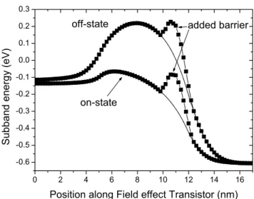
barrier near the end of the channel as shown Fig. 1 for a 7 nm gate length double-gate (DG)
MOSFET. In both on- and off-state conditions this end-channel-barrier enlarges the total
source-drain barrier and then reduces the tunneling transmission. Without this barrier, in
7 nm DG MOSFETs the drive current mainly (~ 80 %) results from the thermionic electrons
whose energy is higher than the source-drain barrier. The influence of the end-channel-barrier
on the drive current Ion is then negligible if the total source-drain barrier is not higher. In the
off-state the tunneling component across source-drain barrier is larger (~ 50 %). Therefore
the reduction of tunneling transmission due to added end-channel-barrier should have larger
consequence on Ioff current. We can expect an increase of on-off ratio as an induced effect of
this added barrier. In the perfect case where the tunneling contribution is completely erased,
an on-off ratio improvement of about 60% can be expected.
In this letter we propose a solution which is close to the solution shown Fig. 1 and which is
conceivable from a technological point of view. Our solution consists in adding an oxide
crenel in the channel as shown in Fig. 2 for a DG MOSFET. This crenel locally increases the
barrier similar to the one described in Fig. 1. The higher the crenel is, the more important the
confinement and the potential barrier will be. In this letter we show a theoretical investigation
of the solution proposed Fig. 2 for a DG MOSFET with a gate length LG = 7 nm, a silicon
thickness TSi = 2 nm and a gate-oxide thickness of 1 nm with a power supply voltage
VD = 0.5 V as suggested by the ITRS for digital applications at low operating power in 2018.1
Our theoretical approach is now described. Due to the importance of 2D transport in this
device, we use a full 2D quantum model based on the non equilibrium Green’s functions
(NEGF) formalism. Within this approach, we adopt the effective mass approximation to write
the Schrödinger equation in which the gate-oxide barriers are assumed to be infinite.
Nevertheless, a 2D quantum transport model is very computationally expensive and the
self-consistence with the Poisson equation is quite difficult to achieve. The 2D transport is then
studied using the electrostatic potential obtained from a mode space solver.6 This last
calculation is performed in a device without crenel. This electrostatic potential is close to the
result of a self-consistent full-2D model because the Si film is very thin and that the crenel is
located in the channel where the electrons density is very low.
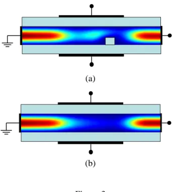
Fig. 3 shows the 2D density of electrons calculated in on-state condition in both Crenel DG
MOSFET and conventional DG MOSFET. (Figure 3: deux lignes…) The influence of crenel
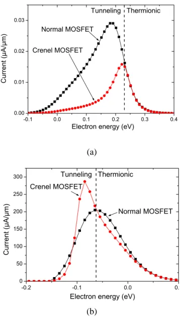
on the current is shown in Fig. 4 where the energy spectrums of the current for normal
MOSFET and Crenel MOSFETs (position p = 5.5 nm) are plotted for both off- and on-state
conditions. In that position the crenel has no influence on thermionic-tunneling border and as
expected the tunneling contribution is reduced by the crenel in the off-state (Fig. 4(a)). We
note a strong decrease of the off-current in device with crenel. Fig. 4(b) shows a surprising
crenel induced increase of the tunneling contribution in the on-state. This very interesting
barrier inducing some peaks in the transmission characteristics (coefficients??) as shown in
Fig. 5.
In order to quantify the crenel induced effect we define two parameters, R and I, respectively
the percentage of on-off ratio and of Ion compared to the values in conventional (without
crenel) DG MOSFET. As expected the best position p of the crenel is found to be at the end
of the channel. When localized near the middle of the channel (p ~ 4 nm) the crenel increases
the thermionic-tunneling border and induces a detrimental decrease of the drive current. The
best position is p ~ 5.5 nm where R is largely higher than 100 % with I ~ 100 %. Concerning
the length l, its influence is insignificant for values ranged between 1 and 3 nm, whereas the
impact of the height h, as shown in Fig. 6 for p = 5.5 nm, is important. The increase of h
induces a strong increase of R combined with a small drive current enhancement. This good
result for drive current, (Fig. 5), is due to quasi-resonant states in barrier potential for the
on-state condition. Of course this effect is limited and the drive current ends up by decreasing
when h is larger than 0.6 nm. A very good compromise is found for h = 0.8 nm (p = 5.5 nm
and l = 1 nm) where I = 98 % and R = 344 % with on-off ratio Ion/Ioff = 1.64 104. This last
value can be compared to both values suggested by ITRS2 3×10⁴ and obtained in this work for the normal DG MOSFET 4.5×10³
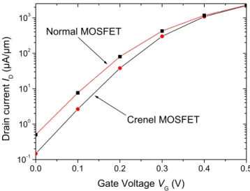
. Fig. 7 shows the ID-VG characteristics calculated in this
crenel MOSFET and in conventional MOSFET.
In conclusion we suggest the use of an oxide crenel in very short DG MOSFET. In order to
reduce the short channel effects, the crenel must be near the end of the channel. It is very
important to well adjust the position and the height of the crenel. For a good parameter
adjustment of the crenel in a 7 nm gate length DG MOSFET our model shows an
improvement of on-off ratio of about 240 % with no significant change for the drive current.
These results go well beyond the best initially expected enhancement (60 %) for the on-off
on-state. The significant advantage of the crenel, because of its physical origin, should not be
reduced by phonon-scattering which are not taken into account in this work. Finally we note
that it is possible to use the crenel in all the multigate structures8 where carriers (electron and
References
1
http://public.itrs.net 2
D. Vasileska, and S. S. Ahmed, IEEE Trans. Electron Devices 52, 227 (2005). 3
A. Svizhenko, M. P. Anantram, T. R. Govindam, B. Biegel, and R. Venugopal, J. Appl.
Phys. 2343 (2002). 4
S. Hasan, J. Wang, and M. Lundstrom, Solid-State Electron. 48, 867 (2004). 5
David K. Ferry, Stephen M. Goodnick, Transport in Nanostructures (Cambridge University
Press, Cambridge, UK, 1999). 6
R. Venugopal, Z. Ren, S. Datta, M.S. Lundstrom, and D. Jovanovic, J Appl. Phys. 92, 3730
(2002). 7
M. Bescond, J.L. Autran, D. Munteanu, and M. Lannoo, Solid-State Electron., 48, 567,
(2004). 8
M. Bescond, K. Nehari, J.L. Autran, N. Cavassilas, D. Munteanu, and M. Lannoo, Tech.
Dig. – Int. Electron Device Meet. 2004, 617. 9
Figure Captions
FIG. 1. First subband along an ultra short metal-oxide-semiconductor-field-effect-transistor
with and without an added potential barrier at the end of the channel. This first subband
(without added barrier) has been obtained with a self-consistent solution of the Poisson
equation and 1D quantum transport equation. The added barrier is schematic. The gate
voltages VG are respectively 0 and 0.5 V for the off- and the on-state with a drain voltage
VD = 0.5 V. The origin of energy is defined by the Fermi level in source.
FIG. 2. Schematic representation of crenel DG MOSFET. The coordinates for the simple
crenel are the position p, the length l and the height h.
FIG. 3. The 2D electron density calculated with our model in (a) a crenel DG MOSFET and
(b) a conventional DG MOSFET for gate voltage and drain voltage given by
VG = VD = 0.5 V.
FIG. 4. Calculated current density versus electron energy (spectrum current) for conventional
and crenel DG MOSFETs (p = 5.5 nm, l = 1 nm, h = 0.8 nm). These spectrums current are
shown for (a) off-state (VG = 0 V) and (b) on-state (VG = 0.5 V), both with VD = 0.5 V. The
tunneling-thermionic border is shown by a dash line.
FIG. 5. Calculated transmission coefficient versus electron energy for conventional and
crenel DG MOSFETs (p = 5.5 nm, l = 1 nm, h = 0.8 nm). These spectrums transmission are
FIG. 6. R and I parameters versus the height h calculated in the crenel DG MOSFET with
p = 5.5 nm and l = 1 nm.
FIG. 7. Calculated drain current ID versus gate voltage VG for conventional and crenel DG
MOSFETs (p = 5.5 nm, l = 1 nm, h = 0.8 nm). These characteristics are calculated with
Figure 1
n+ p h l n+ VG VG VD Figure 2 Cavassilas et al
(a)
(b)
Figure 3 Cavassilas et al
(a)
(b)
Figure 4
(a)
(b)
Figure 5
Figure 6
Figure 7