HAL Id: hal-03041576
https://hal.univ-lille.fr/hal-03041576
Submitted on 5 Dec 2020
HAL is a multi-disciplinary open access
archive for the deposit and dissemination of
sci-entific research documents, whether they are
pub-lished or not. The documents may come from
teaching and research institutions in France or
abroad, or from public or private research centers.
L’archive ouverte pluridisciplinaire HAL, est
destinée au dépôt et à la diffusion de documents
scientifiques de niveau recherche, publiés ou non,
émanant des établissements d’enseignement et de
recherche français ou étrangers, des laboratoires
publics ou privés.
A wide tuning range delay element for event-driven
processing of low-frequency signals in 28-nm FD-SOI
CMOS
Angel Gonzalez, Antoine Frappé, Benoit Larras, Andreas Kaiser, Philippe
Cathelin
To cite this version:
Angel Gonzalez, Antoine Frappé, Benoit Larras, Andreas Kaiser, Philippe Cathelin. A wide tuning
range delay element for event-driven processing of low-frequency signals in 28-nm FD-SOI CMOS.
IEEE Solid-State Circuits Letters, 2020, 3, pp.198-201. �10.1109/LSSC.2020.3010877�. �hal-03041576�
Abstract—This paper presents a widely tunable digital delay element suitable for low-power low-frequency continuous-time digital signal processing systems. The design uses features of the 28 nm FD-SOI CMOS technology to precisely control currents in the pA range and significantly reduce leakage power. The measured tuning range is significantly larger than prior art covering more than 3 decades from 30 ns to 100 µs making it suitable for CT-DSP low frequency filters. At 0.7 V supply voltage, the dynamic power consumption is 15 fJ/event with a residual power consumption due to leakage of 14 pW.
Index Terms—CT-DSP, Digital delay, FD-SOI CMOS, IoT,
Ultra-low-power circuits
I. INTRODUCTION
Ultra-low-power consumption is a major concern for IoT sensors, particularly for those that monitor intermittent signals with short bursts of activity. In this context, event-driven processing emerges as a solution that potentially offers low power consumption by activating processing units only in the presence of information [1]. Continuous-time digital signal processing (CT-DSP) is an event-driven technique that benefits from the robustness and configurability of digital signal processing [2]. Key functions in CT-DSP systems are FIR and IIR filters [3], which rely on precise digital delay lines to set their frequency response. These delay lines, built as a cascade of individual delay elements, approximately represent 70% of the power consumption and area in state-of-the-art CT-DSP systems [4].
A digital delay element designed for CT-DSP systems should offer a wide tuning range and robust operation through handshaking, while power consumption, area, and mismatch should be kept low. Several digital delay element topologies exist in the literature [5]– [8]. However, only the delay presented in [5] achieves a maximum delay value beyond 1 µs at the expense of high energy consumption and large area. Since many IoT applications like voice activity detection, EEG detection, and ECG monitoring require the use of low-frequency filters [9], [10], the CT-DSP implementation of such filters would typically require low-power delay elements with programmable delays from few hundreds of ns to 100 µs. The number of delay taps required to implement a filter is equal to its order, while the number of delays composing each tap varies according to the SNR requirement [4].
Manuscript received May. 15, 2020. This work was supported in part by the European Union with the European Regional Development Fund (FEDER) under Grant NP0007428- 2016_07546 and by the French National Research Agency (ANR-18-CE24-0006-01 LEOPAR).
Antoine Frappé, Benoit Larras and Andreas Kaiser are with Univ. Lille, CNRS, Centrale Lille, Univ. Polytechnique Hauts-de-France, Yncrea Hauts-de-France, UMR 8520 - IEMN, F-59000 Lille, France (1) (e-mail: first.last@yncrea.fr). Philippe Cathelin is with STMicroelectronics SA, Crolles, 38926 Crolles Cedex France (2), (email: philippe.cathelin@st.com) Angel Gonzalez was with (1). He is now with (2), (email: angeldedios.gonzalezsantos@st.com)
This paper presents a new digital delay element implemented in 28 nm UTBB FD-SOI (Ultra-thin body and BOX, fully depleted silicon on insulator) technology. The presented design leverages the advantages of this technology. It offers improved channel control, near-ideal subthreshold slope, low leakage that allows controlling currents smaller than 1 nA, and availability of thick-oxide gate transistors to further reduce leakage currents. The designed digital delay element exhibits a tuning range of more than 3 decades, a maximum delay time of 100 µs, an improved energy consumption (both dynamic and static), high robustness and small silicon area.
The rest of this paper is organized as follows: Section II presents the principles of a digital delay element, while Section III describes in detail the design of the proposed digital delay element. Section IV presents the measurement results and Section V concludes this work.
II. OPERATION OF DELAY ELEMENTS FOR CT-DSP SYSTEMS
In CT-DSP, the information is usually coded into two signals named CHANGE and UD. The first is a short pulse indicating the occurrence of an event, while the second denotes the polarity associated with the level-crossing event. In a CT digital filter, the
CHANGE and UD signals are propagated through delay taps,
constituted by a series of cascaded delay cells to guarantee a fine granularity while providing large delay values.
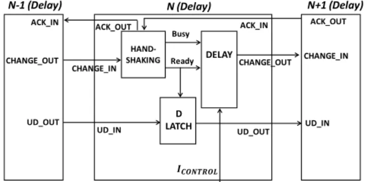
Figure 1 shows the block level schematic of a typical delay cell in a CT digital filter. The delay cell is composed of three blocks: the delay block providing a delay tuned by a control current, the handshaking block to validate the correct propagation of the
CHANGE signal through the delay tap and a D-latch to propagate
the data bit.
ACK_IN ACK_OUT DELAY UD_IN CHANGE_OUT CHANGE_IN Ready Busy D LATCH HAND-SHAKING ACK_IN ACK_OUT CHANGE_IN UD_OUT CHANGE_OUT UD_IN UD_OUT
N-1 (Delay) N (Delay) N+1 (Delay)
Fig. 1. Top level schematic of a delay cell in a CT digital filter
The tunable delay is built around a controlled current source charging or discharging a capacitor. The delay time τ is given by
C
*
V
I
=
(1) where C is the capacitor value, ΔV the voltage excursion across the capacitor, and I the charge (or discharge) current. For a fixed voltage excursion and delay time, low-energy consumption can only be achieved with a very small capacitor, and thus, an ultra-low current.A Wide Tuning Range Delay Element for Event-Driven Processing of
Low-Frequency Signals in 28nm FD-SOI CMOS
Angel González, Antoine Frappé, Senior Member, IEEE, Benoit Larras, Member, IEEE
Andreas Kaiser, Senior Member, IEEE, and Philippe Cathelin
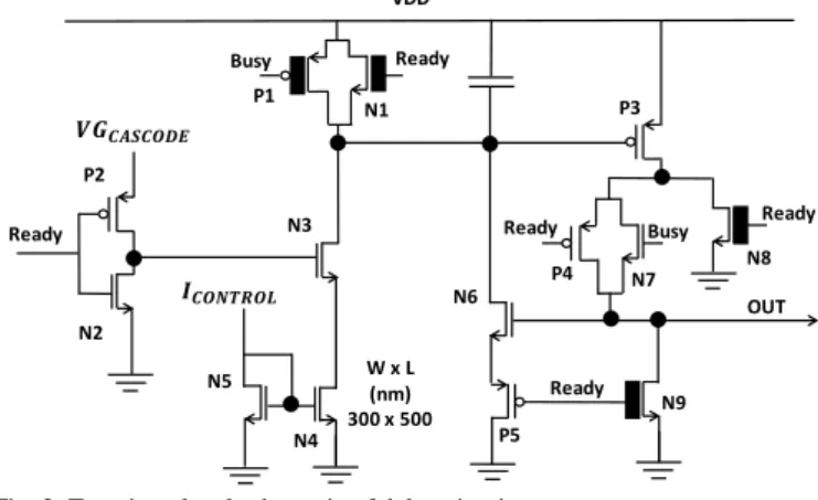
The thyristor-based delay is a very efficient architecture used to implement this principle. The schematic and principle of operation are shown in Figure 2. In the initial state (the Ready signal is at 1 and the Busy signal is at 0), the gate of P3 is connected to VDD and the gate of N6 is connected to ground. When a pulse arrives at the input of the handshaking block, the Busy signal switches on while the Ready signal switches off. The IC current then charges the capacitor and V_CAP starts to decrease. When the capacitor voltage reaches the threshold voltage VTH of P3, OUT starts to rise until N6 turns on, triggering a fast transition of V_CAP and OUT to GND and VDD, respectively. The next delay cell then acknowledges the change at its input and sends back an ACK_IN signal, upon which the Ready and Busy signals return to their initial state. The premise of a thyristor-based delay is to keep power consumption low by using a low current source generated by a transistor in weak inversion; furthermore, thyristor approach gives flexibility on voltage dynamic that can be used to reduce power consumption. However, despite working in weak-inversion none of the existing implementations generates delays longer than 1µs [6]–[8].
Busy OUT VDD τ VDD OUT N4 N6 P3 V_CAP Ready Busy V_CAP Ready Busy Busy τ Ready
Fig. 2. Basic scheme and functioning of the thyristor-based delay
An alternative approach using a tunable inverter to create the delay is presented in [5]. The inverter uses a 5µm length transistor split into 5 fingers of equal length, biased in strong inversion as a current source. This architecture offers the best reported mismatch performance. However, an important penalty is paid in both energy consumption and area. Since our main goal is to keep a low power consumption, we have chosen to implement our delay using a thyristor-based architecture.
III. DELAY ELEMENT DESIGN
Figure 3 shows the schematic of the delay block of our proposed delay-cell. The design strategy was to optimize the current source (N4) controllability in order to reach a large tuning range while reducing dynamic power consumption. Since in event-driven CT DSP filter, the static power contributes largely to the total power consumption, specifically for sparse signals [4], efforts have been made to reduce leakage.
A. Control and generation of currents lower than 1 nA
The fully depleted silicon on insulator (FD-SOI) uses the ultra-thin body and box (UTBB) technology, where the film (silicon above oxide) is very thin (some nm), and the channel is not doped. These characteristics allow to efficiently control the current flow across the transistor channel, while biasing the transistor in subthreshold operation, making possible the control of currents significantly smaller than 1 nA.
To size the NMOS transistor N4 employed as a current source two considerations were taken: the use of a long transistor to reduce the effects of channel length modulation and a W large enough to provide good matching between N4 and N5 for proper current
copy. Transistor dimensions of W=300nm and L=500nm have been chosen. VDD OUT Ready Busy Ready Ready P1 N3 N1 N4 N6 P5 P3 P4 N7 N9 N8 P2 N2 W x L (nm) 300 x 500 Busy Ready Ready N5
DC analysis showed that by biasing the transistor N4 in weak-inversion is possible to control currents between 15pA and 1nA, thanks to a subthreshold slope value of approximately 65mV/decade.
To improve the control of the current during the discharge phase, it is necessary to isolate the current source from the parasitic capacitances of other transistors. For this purpose a cascode transistor N3 has been added. The transistor N3 gate voltage is adjusted to keep N4 saturated over the whole current rage at the expense of a slight increase in the static power consumption of the biasing circuits. An inverter to control the cascode transistor voltage was implemented to turn off N4 in “Ready” mode. Additionally, to improve controllability two of the switches have been implemented as CMOS switches. The CMOS switch formed by transistors P1 and N1 allows to avoid charge injection in the capacitance, when switching to “Busy” mode improving the accuracy of the delay. For the same reason, P4 and N7 form a CMOS switch to avoid charge injection on N6 gate. Input signal dependency was also a major concern of the original delay cell. This mechanism makes the delay dependent on the time between two consecutive CHANGE_IN pulses and is caused by memory effects of internal nodes. Transistor N8 is used for this purpose, forcing drain of P3 to 0V when starting delay operation.
B. Reducing static power consumption
In advanced technology nodes with reduced transistor gate oxide thickness significant gate leakage currents occur due to a phenomenon called thin-oxide gate tunneling, particularly for NMOS transistors. To reduce the static consumption caused by these leakage currents, we implement the switches (P1, N1, N8, and N9) and all logic gates with thick- gate oxide transistors in their low-voltage threshold variant available in the 28nm FD-SOI technology. These transistors drastically reduce the gate leakage currents while exhibiting a threshold voltage around 350mV, which makes them compatible with low voltage operation. The leakage current due to thin oxide gate tunneling has been reduced by approximately a factor 20. The penalties paid for the use of thick-gate oxide transistors are a slight increase in dynamic power consumption and silicon area due to their larger size spacing design rules that apply when combining thick and regular gate oxide transistors.
C. Handshake elements and D latch
The structure employed to perform the handshake is similar to the one proposed by [5] and is shown in Figure 4. The structure is based on the use of a Muller-gate also known as C-element [11]. This gate is similar to a RS flip-flop that changes state whenever both inputs are high or low. The Muller-gate assures that the delay cell is set to the “Ready” state before accepting a new input pulse,
and maintains the ACK_OUT signal low until the output of the previous delay cell is cleared.
Transistor N10 has been added to assure that all delays are properly reset to the “Ready” state during power on-operation.
POWER_ON Ready
C
Ready IN R Q Q __ ACK_IN ACK_OUT N10 Busy RESET HANDSHAKING BLOCK S A B OUT __ __Fig. 4. Handshaking circuit
IV. MEASUREMENTS
A 1.3 mm × 1.3 mm test chip in 28 nm FDSOI CMOS technology has been fabricated. Figure 5 shows the die photo and the layout of the 8.3 µm × 8.9 µm unit delay cell. For characterization purposes, this unit cell is inserted into a sequence of 3 identical cells. An identical structure can be seen in the middle of the chip for on-wafer probe measurements. The die also contains a delay line composed of 8 delay taps, each constituted by 96 unit delay cells, sufficient to implement half the structure of a 16th order FIR filter for a moderate SNR application.
Tap delay line
Unit Delay cells
Handshake
D latch Delay core 8.9 µm
8.3 µm
Fig. 5. Die photo and layout of a unit delay cell
A. Tuning range
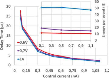
The tuning range of the delay element was evaluated by measuring the time between the rising edges of the UD_IN and UD_OUT signals. Figure 6 shows the measured delay time and dynamic power consumption for several VDDs. It validates the independence of the delay regarding the supply voltage and the independence of the energy per event versus the control current. A VDD of 0.7 V is a good trade-off and is used for the rest of the measurements.
Figure 7 shows the measured delay as a function of the control current for a VDD of 0.7 V for several chips. The extreme points are only available for chip 1. The measured tuning range is from 30 ns to 97 µs.
Input signal dependency has been evaluated using a repetitive input pulse, whose period is spanned from 5 µs to 200 µs. Figure 8 shows the measured input signal dependency on the input pulse period. Despite certain variability of the biasing source it remains below 2% in the worst-case scenario, remaining steady at approximately 0.5% for pulses spaced more than 10µs.
B. Delay error
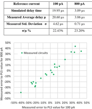
To evaluate the delay variations over multiple dies, the delay time of a unit delay cell was measured for two control currents (100 pA and 800 pA) across 22 different dies from the same wafer. Measurement results are shown in TABLE I. The measured average delay is very close to the simulated value, while the standard deviation is measured to around 20-25%. It is to note that no calibration of any kind is applied here.
To ensure that the delay calibration can be performed for a single reference point, the relation between the relative error on the delay times for currents of 100 pA and 800 pA for each die can be analyzed. Figure 9 shows the relation between these errors for 22 dies. We can observe that the relative delay errors are correlated for the two current settings. If the calibration is performed for a 100 pA current, then the resulting standard deviation when the current is 800 pA is reduced to 5.01%. 0 5 10 15 20 25 30 0 0,15 0,3 0,45 0,6 0,75 0,9 1,05 1,2 Dela y T ime (µ s)
Control current (nA) 0,6V 0,7V 1V 0 10 20 30 40 50 60 0,1 0,3 0,5 0,7 0,9 1,1 Ener gy per ev en t (fJ)
Fig. 6. Measured delay element tuning range for different VDD voltages and measured dynamic power consumption.
0,01 0,1 1 10 100 0,01 0,1 1 10 100 1000 Dela y time (µs)
Control current (nA)
Chip 1 Chip 2 Chip 3
Fig. 7. Measured delay element tuning range for a VDD voltage of 0.7 V.
-2% -1%0% 1% 2% 5 10 20 40 80 160 R ela tiv e dela y diff er ence (%) Input period (µs)
Fig. 8. Measured relative delay difference versus the period of the repetitive input pulses for a delay cell configured at 3.84 µs and a supply voltage of 0.7 V.
C. Unit cells and delay taps mismatches
The local mismatch of delay cells on the same die has been evaluated by measuring the delay value of the taps of the delay line (composed of 8 sections of 96 unit delay cells). The control current is fixed at 5 nA. This measurement has been performed over 3 different circuits. For each circuit, Table II indicates the mean of the 8 measured delays and the standard deviation, as well as the combination of the 3 obtained values.
To calculate the mismatch associated with the unit delay cell, we need to introduce the biasing scheme of the complete delay line. The current mirror (transistor N5) is common for a section of 24 unit delay cells correlating the current deviation of the corresponding delays. The Icontrol for each section are mirror copies of the reference current. Assuming from the simulations of a unit cell that the control current deviation contributes about
delay cell can then be calculated in Table II using the following formula: _ 2 _ 96 , 1 24 1
unit delay tap unit delay tap
P k
k P
=
+ = − (2)The calculated value is consistent with simulation results obtained through 1000 Monte Carlo simulations, where mismatch varied between 9% for a 25pA current to 11% for currents above 100pA.
TABLEI. STATISTICAL ANALYSIS OF DELAY VARIATION DUE TO MISMATCH
Reference current 100 pA 800 pA Simulated delay time 19.95 µs 3.09 µs
Measured Average delay µ 20.60 µs 3.06 µs
Measured Std. Deviation σ 4.62 µs 0.71 µs σ/µ % 22.43% 23.20% -50% -40% -30% -20% -10% 0% 10% 20% 30% 40% 50% -50%-40%-30%-20%-10% 0% 10% 20% 30% 40% 50% Mea sur ed er ro r to P LS v al u e fo r 80 0 p A
Measured error to PLS value for 100 pA Measured circuits
Fig. 9. Statistical dispersion in relative percentage with respect to the simulated values, for 2 control currents measured for 22 circuits
TABLE II.MEASURED MISMATCH FOR DIFFERENT DELAY TAPS
Mean (µs) Std. Deviation/Mean (%) Chip 1 63.17 5.85 Chip 2 63.87 3.61 Chip 3 66.11 4.91 Total (24 points) --- 4.20% Delay Cell 0.67 8.23%
D. Static power consumption
Table III shows the static power consumption of the delay element as a function of the temperature. The measured value was obtained at a temperature of 23°C by measuring the static consumption of the 8 delay taps and dividing by the number of individual delays (768 cells). The static power for the bias circuit is not included.
TABLE III.STATIC POWER CONSUMPTION
Temperature (°C) -20 0 23 40 60
Static power (pW) 7.84 10.57 14.32 50.26 130 Measured value Simulation results
E. Comparison with other works
The comparison of this work with the state-of-the-art is shown in Table IV. This work presents the largest tuning range, the largest absolute delay value and the highest energy efficiency for a delay element with handshaking. This work is also the only one that reports measured mismatch values.
TABLEIV.COMPARISON WITH STATE-OF-THE-ART DELAY CELLS
Parameter [6] [7] [12] [5] This work VDD 1 1.2 1 1.2 0.7 Technology 90nm CMOS - 28nm FD-SOI 65nm CMOS 28nm FD-SOI Tuning range 5 ns – 1 µs 0.3 – 300 ns 15 – 500 ns 5 ns – 10 µs 30 ns - 97 µs Energy/event (fJ) 50 - - 83 15 - 20* 12.5* - 5.4* Area (µm²) 36 - 21* 97 74 σ/µ % - 12.4% - 2.3% 8.23% Hazard-free
handshaking No N/A N/A Yes Yes
Simulation results 100 Monte Carlo simulations *No handshake block and D latch
V. CONCLUSIONS
A digital delay element designed in 28nm UTBB FD-SOI technology has been presented. It achieves a tuning range of more than 3 decades with record maximum delay time of 97µs. The dynamic power consumption is 15fJ/event for a supply voltage of 0.7V and a static power consumption of 14pW while keeping mismatch and area at reasonable values. The proposed delay cell is therefore ideally suited for the implementation of wide tuning
range and extremely low power CT-DSP low-frequency filters. ACKNOWLEDGMENT
The authors thank Mathilde Sie, Patrick Scheer and Jeff Nowakowski from ST Microelectronics for helpful discussions. REFERENCES
[1] C. Weltin-Wu and Y. Tsividis, “An event-driven clockless level-crossing ADC with signal-dependent adaptive resolution,” IEEE J.
Solid-State Circuits, vol. 48, no. 9, pp. 2180–2190, 2013.
[2] Y. Tsividis, “Digital signal processing in continuous time: A possibility for avoiding aliasing and reducing quantization error,” in
2004 IEEE ICASSP, 2004, vol. 2, no. 3, pp. ii-589–92.
[3] Y. Chen, et al., “A Continuous-Time Digital IIR Filter With Signal-Derived Timing and Fully Agile Power Consumption,” IEEE J.
Solid-State Circuits, vol. 53, no. 2, pp. 418–430, 2018.
[4] B. Schell and Y. Tsividis, “A continuous-time ADC/DSP/DAC system with no clock and with activity-dependent power dissipation,”
IEEE J. Solid-State Circuits, vol. 43, no. 11, pp. 2472–2481, 2008.
[5] Y. Chen, R. Manohar, and Y. Tsividis, “Design of tunable digital delay cells,” in 2017 IEEE CICC, 2017, vol. 2017-April, pp. 1–4. [6] B. Schell and Y. Tsividis, “A Low Power Tunable Delay Element
Suitable for Asynchronous Delays of Burst Information,” IEEE J.
Solid-State Circuits, vol. 43, no. 5, pp. 1227–1234, May 2008.
[7] M. Kurchuk and Y. Tsividis, “Energy-efficient asynchronous delay element with wide controllability,” in Proceedings of 2010 IEEE
ISCAS, 2010, pp. 3837–3840.
[8] C. Vezyrtzis, et al., “A Flexible, Event-Driven Digital Filter With Frequency Response Independent of Input Sample Rate,” IEEE J.
Solid-State Circuits, vol. 49, no. 10, pp. 2292–2304, Oct. 2014.
[9] J. Yoo et al., “An 8-Channel Scalable EEG Acquisition SoC With Patient-Specific Seizure Classification and Recording Processor,”
IEEE J. Solid-State Circuits, vol. 48, no. 1, pp. 214–228, Jan. 2013.
[10] K. M. H. Badami, et al., “A 90 nm CMOS, Power-Proportional Acoustic Sensing Frontend for Voice Activity Detection,” IEEE J.
Solid-State Circuits, vol. 51, no. 1, pp. 291–302, Jan. 2016.
[11] J. Sparsø and S. Furber, “Principles of asynchronous circuit design – A systems perspective,” Kluwer Acad. Publ., 2007.
[12] I. Sourikopoulos, A. Frappé, A. Cathelin, L. Clavier, and A. Kaiser, “A digital delay line with coarse/fine tuning through gate/body biasing in 28nm FDSOI,” in ESSCIRC Conference 2016: 42nd