Publisher’s version / Version de l'éditeur:
IEEE Transactions on Instrumentation and Measurement, 58, 4, pp. 853-858,
2009-04
READ THESE TERMS AND CONDITIONS CAREFULLY BEFORE USING THIS WEBSITE. https://nrc-publications.canada.ca/eng/copyright
Vous avez des questions? Nous pouvons vous aider. Pour communiquer directement avec un auteur, consultez la première page de la revue dans laquelle son article a été publié afin de trouver ses coordonnées. Si vous n’arrivez pas à les repérer, communiquez avec nous à [email protected].
Questions? Contact the NRC Publications Archive team at
[email protected]. If you wish to email the authors directly, please see the first page of the publication for their contact information.
This publication could be one of several versions: author’s original, accepted manuscript or the publisher’s version. / La version de cette publication peut être l’une des suivantes : la version prépublication de l’auteur, la version acceptée du manuscrit ou la version de l’éditeur.
For the publisher’s version, please access the DOI link below./ Pour consulter la version de l’éditeur, utilisez le lien DOI ci-dessous.
https://doi.org/10.1109/TIM.2008.2008086
Access and use of this website and the material on it are subject to the Terms and Conditions set forth at
Correction of systematic errors due to the voltage leads in an AC
Josephson Voltage Standard
Filipski, Piotr S.; Kinard, Joseph R.; Lipe, Thomas E.; Tang, Yi-Hua; Benz,
Samuel P.
https://publications-cnrc.canada.ca/fra/droits
L’accès à ce site Web et l’utilisation de son contenu sont assujettis aux conditions présentées dans le site LISEZ CES CONDITIONS ATTENTIVEMENT AVANT D’UTILISER CE SITE WEB.
NRC Publications Record / Notice d'Archives des publications de CNRC:
https://nrc-publications.canada.ca/eng/view/object/?id=848bde35-0377-4db9-9e4e-2c488274e53a https://publications-cnrc.canada.ca/fra/voir/objet/?id=848bde35-0377-4db9-9e4e-2c488274e53a
Abstract— NIST recently reported the first application of a quantum ac Josephson Voltage Standard for calibration of thermal transfer standards in the 1 kHz to 10 kHz frequency range. This paper describes preliminary work on extending its frequency calibration range up to 100 kHz by correcting systematic errors due to voltage leads. A ground loop created by the dc blocks, a previously unaccounted for source of high frequency systematic error, has been identified and its effects partially mitigated.
Index Terms—Quantum-based standard, Josephson arrays, quantization, signal synthesis, standards, superconductor-normal-superconductor devices, voltage measurement.
I. INTRODUCTION
uring the last twelve years, the quantum-based pulse-driven ac Josephson Voltage Standard (ACJVS) has progressed from a concept to a calibration instrument, [1], [2]. The operating principle of such a standard was described in detail in a series of papers [1] - [6]. Very substantial progress has been achieved recently by identifying and reducing the systematic errors, extending the voltage operating range to 300 mV, and extending the frequency range to 100 kHz, [6].
The standard ac voltage is produced by either one or two arrays of Josephson junctions, excited by a synchronized combination of a 15 GHz sine wave and a two-level digital bit stream, clocked at 10 GHz. In response to the bipolar drive signal, a properly excited and biased array (―on margins‖) generates a bipolar output pulse train, in which Manuscript received June 9, 2008. This research was supported by and performed at NIST. Dr. Filipski was visiting NIST as a Guest Researcher.
P. S. Filipski is with the National Research Council, Ottawa, Ontario, Canada, K1A 0R6 (phone: 613-993-2313, fax: 613-952-1394, e-mail: Peter.Filipski@ nrc.ca).
J. R. Kinard, T. E. Lipe, Y.H. Tang are with National Institute of Standards and Technology, Gaithersburg, MD 20899 USA.
S.P. Benz is with National Institute of Standards and Technology, Boulder, CO 80305 USA.
Contribution of the U.S. Government, not protected by U.S. copyright.
the area of each pulse is determined with quantum accuracy. The spectrum of the output pulse train contains low-frequency component(s), such as a pure sine wave or a spectrum of an arbitrarily shaped time waveform that has been converted to a digital binary representation using a delta-sigma modulator algorithm.
The voltage is exactly calculable from knowledge of the modulating code, the pulse frequency and the number of Josephson junctions in the array. The voltage appearing at the input of a device under test (DUT) differs from this calculable value by systematic errors introduced by connections between the junctions and between the arrays and the DUT. The former errors, due to the inductance of superconductive connections between the junctions, were investigated in [6]. In the following we present preliminary investigations of systematic errors due to signals on the voltage leads between the array and the DUT. These frequency-dependent errors can be neglected at 10 kHz and below [2], but must be taken into consideration at higher frequencies.
II. EXPERIMENTALTESTSYSTEM A. Test System
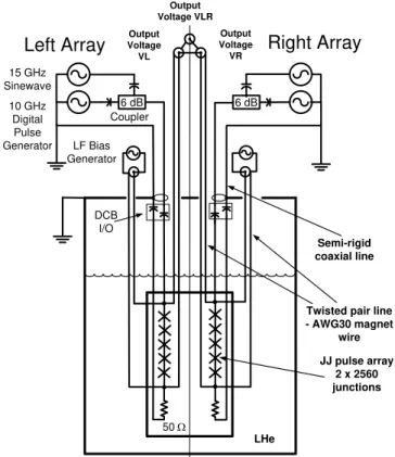
The simplified diagram of the experimental setup, emphasizing connection details significant for the following discussion, is shown in Fig. 1. The source of the quantized ac voltage was a chip containing two independent Josephson arrays of 5120 junctions, ―left‖ and ―right,‖ located inside a liquid helium Dewar. Each array could generate a maximum low-frequency rms ac voltage of 110 mV. Both arrays are energized independently by three voltage sources: a 10 GHz digital code generator (DCG), a 15 GHz sinusoidal continuous wave (CWG), and a low frequency ac bias current generator (AWG). The outputs of the two DCGs are mutually inverted and the arrays generate sine waves with a 180 degree phase shift. All six generators are synchronized to a reference 10 MHz clock. The bipolar exciting pulses are produced by combining the 10 GHz impulse train with a 15 GHz CW in a 6 dB stripline directional coupler. Proper timing between these two signals is achieved by shifting the phase of the continuous wave using a manually adjusted broadband phase shifter (not shown on the schematic.) The output signal of the phase
Correction of Systematic Errors Due to the
Voltage Leads in an AC Josephson Voltage
Standard
Piotr S. Filipski, Senior Member, IEEE, Joseph R. Kinard, Senior Member, IEEE, Thomas E. Lipe,
Member IEEE, Yi-Hua Tang, and Samuel P. Benz, Senior Member, IEEE
applied to the coupler, which was mounted directly on top of a cryoprobe head. The outer conductors of both couplers are connected and grounded through the cryoprobe and the Dewar. The semi-rigid coaxial lines, supplying high frequency pulses to the arrays, are isolated from the couplers by inner/outer dc blocks (DCBs). Two separate twisted-pair lines (TPLs), made of copper wire, connect each array to low-frequency terminals at the top head of the cryoprobe. One pair supplies an array with the input bias current; the second pair transmits the quantized ac voltage to the room temperature outputs of the left and right arrays respectively, VL and VR. The current and voltage leads are not connected to the array terminals directly but through four, one in each lead, on-chip inductive low pass filters [7]. These filters (not shown) attenuate high frequency harmonics, inherent to the principle of operation of the quantum standard. The bias currents are generated by AWGs, followed by battery-operated, floating, variable-gain transconductance amplifiers (not shown).
Outputs of the two arrays can be connected in series, doubling the rms output voltage to 220 mV, output VLR in Fig. 1. The calibrated DUT was a commercial, amplifier-aided, ac-dc thermal transfer standard (TTS.) Its input was connected to the output of the cryoprobe through a coaxial RG-58 cable. The total length of the cable, partially wound on a magnetic core to form a current equalizer (coaxer,) was 1.68 m.
B. Voltage Lead Parameters
The two output voltage TPLs, of an approximate length of 1.30 m, were not identical, probably due to an unequal twisting. Their average parallel capacitance and series inductance, measured at 20 kHz, were 141 pF and 0.63 μH. An average series resistance of the TPL, when the array was immersed in the liquid helium was 0.37 Ω, less than half of its room temperature resistance. Catalog equivalent parameters of a RG-58 coaxial cable are 101 pF/m, 0.25 μH/m, and 0.049 Ω/m. The coaxial cable parameters can be considered as frequency independent in the tests discussed in this paper; variations from the assumed catalog values (up to ±10 %) were taken into account in the uncertainty budget.
III. RESULTSOFSIMULATIONSANDTESTS
A. Output Spectrum
The calculable sinusoidal waveform generated at the output of a pulse driven Josephson array is accompanied by high frequency digitization harmonics. As an example, Fig. 2 shows a calculated spectrum of a delta-sigma modulated two-level bit stream. The high frequency harmonics have to be filtered out to ensure they do not contribute to the low frequency rms signal. Fortunately, this task is straightforward because the digitization noise
The intrinsic low-pass filters, including the on-chip filters mentioned above and that created by reactances of the voltage leads, loaded by the TTS, attenuate the digitization harmonics significantly. Fig. 3 shows an example of a spectrum observed at the rms output of a single array (output VL) generating a 100 mV sinusoidal voltage at 100 kHz. At frequencies below 500 MHz, no digitization harmonics greater than –55 dBm were observed. The instrument used was a commercial network/spectrum analyzer, connected in parallel to the TTS.
The sensitivity of the calibrated TTS also decreases with frequency and was evaluated by applying a high frequency test signal from a calibrated generator to the input, and measuring the dc output signal. The results for three instruments, manufactured at different times, are shown in Fig 4. The TTS frequency response above 1 MHz corresponds approximately to a first-order low-pass filter with a 10 MHz, -3 dB corner frequency, further reducing requirement for the digitization harmonics filtering.
Presence of the low-pass filter at the input of the transfer standard improves the repeatability of the ac-dc transfer measurements by reducing the digitization harmonics noise signal. For this reason, previously, the most accurate measurements below 10 kHz were conducted with an additional LC filter, usually a 3-pole, Butterworth-type, with 3 MHz cut-off frequency, [1], [4]. However, in the tests of frequencies up to 100 kHz discussed in this paper, we decided to minimize the attenuation of the signal from any additional filtering. So, in the tests reported here we either used no filter between the ACJVS and the TTS or just a simple first-order RC filter (–3 dB at 15 MHz), shown in Fig. 5 by the broken line. The signal attenuation by a divider formed by a series resistance (50 of the RC filter and the frequency dependent input resistance of the TTS was less than 25 V/V at 100 kHz.
B. Lead Modeling and SPICE Simulations
The voltage drops on the voltage leads loaded by a TTS were evaluated using SPICE1 simulations, using the TPL and the coaxial line parameters given in Section II. The model used is shown in Fig. 5. The total internal reactance of the JJ array, LJJ, was determined experimentally from two measurements, subtracting measured inductance of the shorted TPL from the inductance of the TPL connected to a superconducting chip. The average value for right and left arrays was 0.125 H. The TPLs and the coaxial cable were modeled by 5 lumped-element T-sections of the R-L-C-L-R type. The TTS was modeled as a parallel RC circuit. Its parameters were determined experimentally. The TTS input resistance is frequency dependent; for the tested TTS it changed from 8.5 M at 2.5 kHz to 2.1 M at 100 kHz.
1 Commercial software is identified in this paper only in order to adequately specify the experimental procedure. Such identification does not imply recommendation or endorsement by the National Institute of Standards and Technology, nor does it imply that the equipment identified are necessarily the best available for the purpose.
The results of the simulations are shown in Fig. 6. A curve marked ―single array, TPL only‖ shows calculated relative voltage rise over the theoretical array-generated voltage, at the output of the TPL, VL or VR, and loaded solely by the TTS. The TTS input reference plane is thus situated directly at the cryoprobe head. This calculated voltage rise varied from 0 V/V at 10 kHz to 39 V/V at 100 kHz. The remaining curves present results obtained with the additional coaxial cable between the cryoprobe output and the TTS input, and with or without a 15 MHz RC filter in between them. The last curve shows the voltage rise on leads of the two arrays connected in series at the output marked VLR.
The validity of the simulations was verified experimentally. Several TPLs were assembled, replicating TPL in the cryoprobe, and the voltage rises on such lines, loaded by the TTS, TTS and coaxial cable with and without a filter, were measured. For example, for the TPL only, at 100 kHz the measured voltage rise varied from 23 V/V to 29 V/V, depending on the residual parameters of the line. In the simulations, the on-chip inductance was taken into account, not present in the measurements. This explains why the measured values are somewhat lower than obtained by simulation.
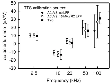
C. AC-DC Transfer Difference Calibrations of TTS Fig. 7 shows a frequency characteristic of the ac-dc transfer difference of a TTS at 100 mV using the single array as a reference at either output VL or VR. The characteristic was determined in two steps: an ac-dc difference at 2.5 kHz and an ac-ac difference at higher frequencies. The SPICE-calculated lead voltage rise was used as a correction, i.e. it was assumed that the ac voltage at the input of the TTS was equal to the theoretical ac voltage generated by an array augmented by the calculated lead voltage rise. The measurements were repeated twice, with and without an RC filter. This TTS was previously calibrated at the National Research Council Canada using a thermal voltage converter (TVC,) with results shown on the graph as a third set of points.
At 2.5 kHz, the standard uncertainty of the ac-dc transfer calibrations using the ACJVS was derived in [2]. For higher frequencies the influence of the following error sources was additionally taken into account: test repeatability, residual systematic errors due to the intrinsic array inductance, [6], and lead voltage correction.
At 2.5 kHz the expanded calibration uncertainty using the ACJVS is 2 V/V, which is lower than the best NRC calibration uncertainty, 5 V/V. At 100 kHz the situation is reversed, the TVC-based calibration uncertainty, 7 V/V is lower than the ACJVS-based, 20 V/V. However, above 20 kHz the ACJVS lead correction uncertainty dominates the uncertainty budget. It can be significantly decreased by careful measurements and stabilization of the lead parameters.
Comparison of the two methods of TTS calibration, using either the ACJVS or a TVC as a standard, shows very good agreement. At higher frequencies this agreement improves when a low-pass filter is used at the ACJVS output. This indicates that the influence of the residual digitization harmonics should be included in the uncertainty budget.
D. Ground Loop Systematic Error
When the two arrays are connected in series, in order to double the rms voltage to 200 mV, the length of the voltage leads also doubles, as in Fig. 1, and the systematic lead error increases. The calculations show that at 100 kHz it increases from 94 V/V, for a single array, to 147 V/V for two arrays in series, Fig. 6. However, when the two arrays were connected galvanicaly at the top of the cryoprobe, creating the series connection, the observed output voltages changed significantly more than expected, [8]. The measured error was significantly larger than the expected lead error, in particular, at 100 kHz the error was up to 5 times larger. This behavior persisted when the two arrays located on the common substrate of a single chip were replaced by two arrays located on two separate chips.
We traced the source of this interaction between the arrays to a ground loop created by the outer capacitors of the 10 MHz dc blocks grounded at the cryoprobe. Fig. 8 shows the circuit model that includes the ground loop consisting of the dc block capacitance CDCB, the outer conductors of the semi-rigid microwave lines, the 50 terminating resistors, and the link between the arrays, Llink. The loop current creates voltage drops on the residual parameters of the TPLs and inductances of the arrays. Consequently, when the two arrays are connected in series, the equivalent circuit of the voltage leads has to include the above-mentioned capacitances of the dc blocks as well as capacitances from the TPLs to ground, CTGN, Fig. 8. To a large extent this additional error can be accurately estimated, as shown in Fig. 9. The plots for a 10 MHz dc block show the combined lead and ground-loop systematic errors measured experimentally and calculated from the equivalent circuit. The TPLs and the coaxial line were modeled as previously.
By experimenting with a different chip, it was possible to decrease this ground-loop error significantly by replacing the 10 MHz dc block with a 500 MHz dc block, which decreases CDCB from 4.5 nF to 60 pF. Calculations for a 500 MHz dc block shown in Fig. 9 indicate that the ground loop error becomes significantly less than the leads error alone. At 100 kHz the calculated lead error was 147 V/V and the combined leads and ground loop error was 163 V/V. Unfortunately, this change simultaneously decreased the array operating margin. For a 200 mV array the operating margin decreased below the 1 mA required for reliable operation.
We also used ferrite coaxers to additionally decrease the ground loop current. This approach was less successful, because the present design of the cryoprobe head does not provide much room for inclusion of large magnetic cores.
When ACJVS is used as a calibrator, the voltage appearing at the input reference plane of the DUT differs from the theoretical value by systematic errors introduced by connections between the standard and the DUT. We showed in this paper that these systematic errors could be successfully calculated from the impedance of the voltage leads. We also identified a new source of calibration error that is due to a ground loop created by the dc blocks when the two arrays are connected in series to double the output voltage. Future work will concentrate on reduction of this ground-loop systematic error.
REFERENCES
[1] S.P. Benz and C.A. Hamilton, ―A Pulse-Driven Programmable Josephson Voltage Standard,‖ Appl. Phys. Lett., vol. 68, no. 22, May 1996, pp. 3171-3173.
[2] T.E. Lipe, J.R. Kinard, Y.H. Tang, S.P. Benz, C.J. Burroughs and P. Dresselhaus. ―Thermal Voltage Converter Calibrations Using a Quantum AC Standard,‖ Metrologia, vol.45, no.3, pp..275-280, June 2008.
[3] C.J. Burroughs, S.P. Benz, P.D. Dresselhaus, and Y. Ching, ―Precision Measurements of AC Josephson Voltage Standard Operating Margins,‖ IEEE Trans. Instrum. Meas., vol. 54, no. 2, pp. 624-627, April 2005
[4] S.P. Benz, C.J. Burroughs, P.D. Dresselhaus, N.F. Bergren, T.E. Lipe, J.R. Kinard, and Y. Tang, ―An AC Josephson Voltage Standard for AC-DC Transfer-Standard Measurements,‖ IEEE Trans. Instrum. Meas., vol. 56, no. 2, pp. 239-243, April 2007
[5] O. F. Kieler, R. P. Landim, S.P. Benz, P. D. Dresselhaus, C. J. Burroughs, ―AC-DC transfer standard measurements and generalized compensation with the ac Josephson voltage standard,‖ IEEE Trans. Instrum. Meas., vol. 57, no. 4, pp. 791-796, April 2008.
[6] R. P. Landim, S. P. Benz, P. D. Dresselhaus, and C. J. Burroughs, ―Systematic-error signals in the ac Josephson voltage standard: measurement and reduction,‖ IEEE Trans. Inst. Meas., vol. 57, no. 6, pp. 1215-1220, June 2008.
[7] M. Watanabe, P.D. Dresselhaus, S.P. Benz, ―Resonance-Free Low-Pass Filters for the AC Josephson Voltage Standard,‖ IEEE Trans. Applied Superconductivity, vol. 16, No.1 pp. 49-52, March 2006. [8] P.S. Filipski, J.R. Kinard, T.E. Lipe, Y.H. Tang and S.P. Benz,
―Correction of Systematic Errors due to Voltage Leads in AC Josephson Voltage Standard,‖ [CD] Proc. CPEM 2008, Boulder, CO USA, June 2008, paper ThP-62, 2 pages.
50 6 dB 6 dB 15 GHz Sinewave 10 GHz Digital Pulse Generator Output Voltage VR Output Voltage VL
Right Array
Left Array
Twisted pair line - AWG30 magnet wire Output Voltage VLR LF Bias Generator DCB I/O Coupler JJ pulse array 2 x 2560 junctions Semi-rigid coaxial line LHe
Fig. 1. Simplified circuit diagram of the ACJVS. DCB I/O indicates the inner/outer dc block, LHe indicates the liquid helium Dewar.
Fig. 3. Spectrum observed at the output of a single array generating 100 mV at 100 kHz, measurement range 500 MHz, resolution bandwidth 10 kHz.
Fig. 2. Calculated frequency spectrum of a digital code for a 100 kHz delta-sigma modulated sinusoidal waveform that is 89% of full scale.
fs – sampling frequency, frep – pattern repetition frequency, M – pattern memory size, f = nfs/M – signal frequency, n- number of periods in a pattern.
Frequency (MHz) 0.1 1 10 100 Ou tput voltage chang e ( dB) -40 -30 -20 -10 0 10 TTS #1, TTS#3 TTS #2
10 MHz 1st order low pass filter
Fig. 4. Frequency characteristics of three different thermal transfer standards compared with a theoretical characteristic of a first-order 10-MHz low pass filter.
LJJ LPF CLPF RLPF 5 segments 5 segments TTS CTTS RTTS
Twisted pair line JJ Array
RC LPF Coaxial line
VL
Fig. 5. Model of the output voltage leads. See description in the text. Frequency (kHz) 10 20 50 70 100 O ut put vo lta ge ch ang e ( V/ V) -20 0 20 40 60 80 100 120 140 160
single array, TPL only single array, TPL + coaxial cable single array, TPL + LPF + coaxial cable two arrays in series, TPLs + coaxial cable
Fig. 6. SPICE simulations; frequency characteristic of the ACJVS output voltage loaded by a TTS. See description in the text. Frequency (kHz) 2.5 10 20 50 100 ac-dc differ ence ( V/V) -30 -20 -10 0 10 20 30 40 50 ACJVS, no LPF ACJVS, 15 MHz RC LPF TVC TTS calibration source:
Fig. 7. Ac-dc transfer calibration of a TTS using an ACJVS with no LPF, with an RC LPF, and a TVC. Lead corrections were applied. Error bars indicate the expanded uncertainty.
LJJ TPL Left CTTS RTTS CTGnd CTGnd R50 CDCB Llink LJJ TPL Right CTGnd CTGnd R50 CDCB
Left array Right array
Fig. 8. Model of connections of two arrays showing ground loop created by the dc blocks.
Frequency (kHz) 10 20 50 70 100 Out put vol tage change ( V/V) 0 200 400 600 800 1000 calculated - 10 MHz dc block measured - 10 MHz dc block calculated - 500 MHz dc block calculated - no ground loop
Fig. 9. Calculation of the ground loop influence for two different dc blocks.
Piotr S. Filipski (M’84-SM’90) received the M.S. and Ph.D. degrees in electrical engineering from the Silesian Technical University (STU), Gliwice, Poland, in 1972 and 1977, respectively, where he worked from 1972 to 1981.
In 1981 he joined the staff of the Power Engineering Section of the Electrical Engineering Division, National Research Council of Canada, where he was involved in development of measurement techniques and instrumentation for measurement of active and reactive power, particularly in nonsinusoidal situations. He is presently a Senior Research Officer in the Electrical Standards Group of the Institute for the National Measurement Standards, National Research Council. His current research is aimed at the high precision ac-dc transfer measurements. Recently, he has spent 3 months as a Guest Researcher at the NIST Quantum Electrical Metrology Division in Gaithersburg, working on the characterization of a transmission line in an ACJVS.
Dr. Filipski is a former Ottawa Chapter Chairman of the IM Society of IEEE, a former IEEE Ottawa Section Chairman and a Registered Professional Engineer of the province of Ontario, Canada.
Joseph R. Kinard (SM’07) received degrees in physics from Florida State University, Tallahassee, and from the University of Massachusetts, Amherst. He first joined the staff of the Electricity Division, National Bureau of Standards [later the National Institute of Standards and Technology (NIST)], Gaithersburg, MD, in 1963 and worked in dielectrics and absolute electrical measurements. From 1971 to 1983, he was with the University of New South Wales, Sydney, Australia, where he was active in a wide range of ac, dc, and RF electrical measurements and calibrations. He was a Guest Lecturer at the New South Wales Institute of Technology, Sydney (now University of Technology, Sydney). Since his return to NIST in 1983, he has been working in the areas of quantum ac and thermal transfer standards, including the application of new technologies to improve primary and working, ac–dc transfer standards. He has served on assessment teams for the National Voluntary Laboratory Accreditation Program, USA, and the National Association of Testing Authorities, Australia.
Mr. Kinard is the author of over 60 technical papers. He holds two patents and is the recipient of a U.S. Department of Commerce Gold Medal, two Silver Medals, and the R&D 100 Award.
Thomas E. Lipe (M’88) is the Leader of the Ac-dc Difference Standards and Measurement Techniques Project at NIST. Mr. Lipe received the B.S. degree in physics from East Carolina University, Greenville, NC, in 1980 and the M.S. degree, also in physics, from the Catholic University of America, Washington, DC, in 1994. He joined the staff of NIST (then NBS) in 1983 where he designed and constructed the first automated system for the routine measurement of thermal converters. His present research interests include quantum ac voltage standards, fabrication of new thermal converters using semiconductor fabrication techniques, and the use of cryogenic standards for ac-dc difference metrology. Mr. Lipe occasionally teaches Electrical Engineering at Montgomery College in Rockville, MD. He shared the 2007 US Department of Commerce Gold Medal for the development and dissemination of the world’s first quantum based electrical standard for ac voltage, and has authored over forty technical papers. He is also an assessor for NVLAP.
Yi-hua Tang received the Ph.D. degree in low temperature physics from the University of Florida, Gainesville, in 1987.
He worked in the private sector from 1991 to 1996 in the field of Josephson arrays and voltage standards. In January 1997, he joined the Quantum Electrical Metrology Division, National Institute of Standards and Technology (NIST), Gaithersburg, MD, where he is currently working on the Josephson voltage standard and its applications in metrology. He is responsible for maintaining the U.S. legal volt and providing for the dissemination of an internationally consistent and traceable voltage standard tied to the SI units. His research interest is to develop applications of Josephson technology for dc and ac voltage metrology.
Dr. Tang is a member of the American Physical Society.
Samuel P. Benz (M’01–SM’00) was born in Dubuque, IA, on December 4, 1962. He received the B.A. degree (summa cum laude) in physics and math from Luther College, Decorah, IA, in 1985 and the M.A. and Ph.D.
degrees in physics from Harvard University, Cambridge, MA, in 1987 and 1990, respectively. He was awarded an R.J. McElroy Fellowship (1985– 1988) to work toward the Ph.D. degree.
In 1990, he joined the National Institute of Standards and Technology (NIST), Boulder, CO, as a NIST/NRC Postdoctoral Fellow and became a permanent Staff Member in January 1992. He has been the Project Leader of the Quantum Voltage Project at NIST since October 1999. He has worked on a broad range of topics within the field of superconducting electronics, including Josephson junction array oscillators, single flux quantum logic, ac and dc Josephson voltage standards, and Josephson waveform synthesis. He has 150 publications and is the holder of three patents in the field of superconducting electronics.
Dr. Benz is a member of Phi Beta Kappa and Sigma Pi Sigma. He was the recipient of two U.S. Department of Commerce Gold Medals for Distinguished Achievement.