Publisher’s version / Version de l'éditeur:
The Journal Physical Chemistry C, 113, 40, p. 17296–17300, 2009-09-04
READ THESE TERMS AND CONDITIONS CAREFULLY BEFORE USING THIS WEBSITE.
https://nrc-publications.canada.ca/eng/copyright
Vous avez des questions? Nous pouvons vous aider. Pour communiquer directement avec un auteur, consultez la première page de la revue dans laquelle son article a été publié afin de trouver ses coordonnées. Si vous n’arrivez pas à les repérer, communiquez avec nous à [email protected].
Questions? Contact the NRC Publications Archive team at
[email protected]. If you wish to email the authors directly, please see the first page of the publication for their contact information.
NRC Publications Archive
Archives des publications du CNRC
This publication could be one of several versions: author’s original, accepted manuscript or the publisher’s version. / La version de cette publication peut être l’une des suivantes : la version prépublication de l’auteur, la version acceptée du manuscrit ou la version de l’éditeur.
For the publisher’s version, please access the DOI link below./ Pour consulter la version de l’éditeur, utilisez le lien DOI ci-dessous.
https://doi.org/10.1021/jp9038607
Access and use of this website and the material on it are subject to the Terms and Conditions set forth at
Plastic substrates for surface-enhanced Raman scattering
Geissler, Matthias; Li, Kebin; Cui, Bo; Clime, Liviu; Veres, Teodor
https://publications-cnrc.canada.ca/fra/droits
L’accès à ce site Web et l’utilisation de son contenu sont assujettis aux conditions présentées dans le site LISEZ CES CONDITIONS ATTENTIVEMENT AVANT D’UTILISER CE SITE WEB.
NRC Publications Record / Notice d'Archives des publications de CNRC:
https://nrc-publications.canada.ca/eng/view/object/?id=bc7dba0c-7a85-42d3-81ed-44a3608beb68 https://publications-cnrc.canada.ca/fra/voir/objet/?id=bc7dba0c-7a85-42d3-81ed-44a3608beb68Plastic Substrates for Surface-Enhanced Raman Scattering
Matthias Geissler,* Kebin Li, Bo Cui, Liviu Clime, and Teodor Veres Conseil national de recherches Canada, Institut des mate´riaux industriels, BoucherVille, Québec J4B 6Y4, Canada
ReceiVed: April 27, 2009; ReVised Manuscript ReceiVed: July 20, 2009
This paper investigates the fabrication of substrates for surface-enhanced Raman scattering (SERS) using hard thermoplastic polymers in conjunction with sputtering and electroless deposition of a thin Au or Ag film. In contrast to silicon or glass, plastic materials promote the replication of nanoscale structures over large areas in a rapid and cost-effective manner using molding or embossing techniques. However, synthetic polymers are Raman-active compounds, providing a source of interference with signals arising from reporter molecules that may be used for SERS detection. Moreover, most plastics melt and undergo degradation when exposed to a focused laser beam, resulting in irreversible loss of the SERS-active metal features in the detection area. We address these issues and show that proper decoration of the plastic surface with a metal overlayer can suppress Raman background signal of the polymer substrate, as well as any adverse effect arising from laser illumination.
Introduction
SERS is an optical detection method that reveals structural information of chemical and biological molecules attached to Au or Ag nanostructures.1,2 It is generally accepted that
SERS involves localized plasmonic resonances and vibrations of molecules that interact with the monochromatic light, causing a shift in frequency of the scattered photons. While these changes in frequency are determined by the excitation energy of the vibrational modes of a particular molecule, enhancement of the corresponding signals depends on physi-cal parameters of the nanostructures such as their size, shape, and degree of aggregation. Local plasmonic coupling between resonant nanostructures (commonly called “hot spots”) can further enhance the electromagnetic field by several orders of magnitude compared to those of individual ones.3,4
Moreover, it is possible to tune SERS activity by adjusting the geometry of the nanostructured substrate with respect to the wavelength and orientation of the laser light used for excitation.5,6 One approach to producing SERS-active
sub-strates uses aggregation of metal nanoparticles, such as colloidal spheres,7wires,8or cubes9on solid supports. Such
systems are known to provide strong enhancement but are difficult to control and therefore remain poorly reproducible. Nanofabrication in conjunction with metal deposition is another approach which appears to circumvent this drawback,5,6
providing a promising solution toward integrated analytical platforms based on SERS.
The fabrication of SERS-active substrates typically comprises silicon as a solid support since micro- and nanolithographic methods involving resist, development, and pattern transfer procedures are well established for this material. However, machining of silicon is an elaborate process and requires access to sophisticated equipment, which is detrimental to the fabrica-tion of disposable, low-cost chips for SERS applicafabrica-tions. Plastic materials may therefore provide a plausible alternative, as they promote replication of nanoscale structures over large areas in
a rapid and cost-effective manner and potentially facilitate their integration in lab-on-a-chip (LOC)10,11devices. While
polymer-based supports have attracted increasing attention in a number of scientific and technological areas, including organic electron-ics,12array-based DNA detection,13and tissue engineering,14they
are rarely being used in SERS, as suggested by the limited number of publications dealing with this topic.15-21Previously,
SERS measurements have been reported for nanostructured substrates fabricated from polyvinylchloride,15
poly(dimethyl-siloxane),16and polystyrene (PS),18for example, using molding
or embossing techniques. In addition, arrays formed from PS nanospheres coated with a thin metal film have been shown to provide effective SERS substrates responding to a range of excitation wavelengths.19 Lee and co-workers have employed
thermoresponsive polymer membranes in conjunction with metal nanoparticle films as a means of tuning SERS activity.17The
use of polymer scaffolds seeded with Au or Ag nanoparticles20
and hybrid structures comprising metal-coated particles embed-ded in a polymer matrix21have also been explored to this end.
However, implementation of plastic materials as SERS platforms is by no means straightforward since an number of synthetic polymers such as PS, polycarbonate (PC), and poly(methyl-methacrylate) (PMMA) are Raman-active compounds22-25
(Fig-ure 1), providing a source of interference with signals arising from reporter molecules that are used for SERS detection. In addition, most plastics melt and/or chemically degrade (“burn”) upon exposure with a focused laser beam, resulting in irrevers-ible loss of the SERS-active metal features in the detection area. This paper is responding to these issues, demonstrating that proper decoration of the plastic surface with a metal overlayer provides a meaningful way to suppress Raman background signal of the polymer substrate, as well as any adverse effect during laser illumination.
Experimental Section
Preparation of Substrates.PMMA slides (25 × 75 mm2in
area, 1 mm in thickness) were prepared by injection molding of Plexiglas VS UVT (Altuglas International, Philadelphia, PA) using a Boy 30A injection tool (Dr. Boy GmbH,
Neustadt-* To whom correspondence should be addressed. Phone: +1 450 641-5388. Fax: +1 450 641-5105. E-mail: [email protected].
J. Phys. Chem. C 2009, 113,
17296
10.1021/jp9038607 CCC: $40.75 Published 2009 by the American Chemical Society Published on Web 09/04/2009
Fernthal, Germany) operated at a temperature of 220-240 °C, an injection speed of 30 mm s-1
, and a pressure of 132 bar. The mold (stainless steel, custom-fabricated) was cooled for 15 s before the slide was released. PS slides were prepared by hot embossing of PS pellets (MW ) 105, Alfa Aesar, Ward
Hill, MA) against two silicon wafers (serving as top and bottom plates, respectively) using an EVG 520 embossing tool (EV Group, Scha¨rding, Austria) operated at a temperature of 170 °C and an applied force of 10 kN. PC sheets were obtained from Modern Plastics, Inc. (Bridgeport, CT) and were used as received.
Fabrication of Nanohole Arrays. Nanohole arrays were fabricated by nanoimprint lithography (NIL) using an EVG 520 embossing tool (EV Group) and a pillar array engraved into SiO2that was thermally grown on a silicon wafer. Pillars were
100 nm wide, 80-200 nm in height, and were arranged with a pitch of 200 nm. PMMA pellets were sandwiched between the master and a planar silicon wafer covering an area of ∼30 cm2.
Upon heating of the stack to 160 °C, a force of 1.5 kN was applied for 2 min followed by evacuation of the system to below 1 Torr. Then, a force of 10 kN was applied for 5 min before the system was vented and cooled to ∼90 °C. The thickness of resultant PMMA sheets was ∼200 µm. To facilitate separation, both wafers were coated with an antiadhesion layer using 1H,1H,2H,2H-perfluorooctyltrichlorosilane (Sigma-Aldrich Corp., St. Louis, MO) which was deposited from the vapor phase under reduced pressure. Resultant sheets were fixed on a standard PMMA slide using epoxy resin to maintain stability and ensure proper handling of these fragile substrates. All fabrication steps were carried out in a clean room environment (class 1000).
Metal Deposition and Immobilization of Probes. Metal films were deposited using a DC/RF Magnetron sputter system (Kurt J. Lesker, Clairton, PA) at a rate of 0.2 Å s-1. Ag and Au
sputter targets were obtained from Kurt J. Lesker and had a purity of 99.999% and 99.99%, respectively. Electroless deposi-tion (ELD) was done using an aqueous silver staining soludeposi-tion composed of 0.02 M AgNO3(Alfa Aesar), 0.33 M citric acid
(Sigma-Aldrich), and 0.19 M hydroquinone (Sigma-Aldrich).26
The mixture was prepared prior to use and operated at room temperature without agitation. Plastic slides were primed by sputtering a thin layer (e.g., 2 Å) of Au serving as a catalyst. Substrates were typically immersed in the staining solution for 5-10 min. Immobilization of 4-mercaptopyridine (4-MPy, Sigma Aldrich) on metal-coated substrates was done by incuba-tion with a 2.0 mM aqueous soluincuba-tion for 10 min, followed by rinsing with DI water and drying with a stream of nitrogen gas. Instrumentation. Raman spectra were acquired using a Raman Micro Station R3 (Avalon Instruments, Boston, MA) equipped with a 40× objective lens coupled to a diode laser source (OEM Laser Systems, Inc., East Lansing, MI) with an emission wavelength ofλ ) 785 nm. The spot diameter was 25µm providing a power density of 0.15 mW µm-2
. Spectra were calibrated with respect to the Raman band of silicon at 521 cm-1
. Measurements of optical transmittance (T) were performed with a Lambda 950 UV/vis Spectrometer (Perkin-Elmer, Waltham, MA) using an uncoated plastic slide as a reference. Atomic force microscopy (AFM) measurements were done using a multimode Nanoscope IV instrument (Veeco Metrology Group, Santa Barbara, CA), operated at ambient conditions and in contact mode using silicon nitride cantilevers (NP-S20, Veeco) with a spring constant of 0.58 N m-1. Each
sample was imaged at a rate of ∼1.0 Hz using a pixel resolution of 512 × 512. Scanning electron microscope (SEM) images were taken using an S-4800 scanning electron microscope (Hitachi, Mississauga, ON) operated at an acceleration voltage of 5.0 kV.
Results and Discussion
In a first set of experiments, we sputter-coated planar slides of PMMA with Ag films ranging from 5 to 50 nm in thickness, and acquired the corresponding Raman spectra (Figure 2). As shown in Figure 2A, a notable reduction of the signal strength can be observed when the slides are coated with Ag films of 5 and 15 nm in thickness. No Raman signals were detected for slides covered by 30 nm of Ag. Figure 2B reveals the trend for
Figure 1. Raman spectra of selected hard thermoplastic materials along with formula of their respective monomer units. (A) PS. Major bands: 622 cm-1in-plane ring deformation; 1000 cm-1(C-C) stretch; 1032
cm-1(C-H) in-plane bending, and 1600 cm-1(C-C) stretch.23(B)
PC. Major bands: 636 cm-1in-plane ring deformation; 706 cm-1
out-of-plane ring deformation; 888 cm-1 (C-CH
3) stretch; 1112 cm-1
(C-H) in-plane bending; 1178 cm-1(C-H) in-plane bending; 1234
cm-1(O-CdO) stretch; 1604 cm-1ring stretch.24(C) PMMA. Major
bands: 600 cm-1(C-C-O) stretch; 812 cm-1(C-O-C) stretch; 988
cm-1(O-CH
3) rocking; 1452 cm-1(C-H) in-plane bending; and 1728
cm-1(CdO) stretch.22
the Raman mode at 812 cm-1
in a comparative manner. The data suggest that 20 nm corresponds to a minimum film thickness required for shielding the plastic surface effectively from illumination, which is in general agreement with previous studies, confirming that Ag deposits below 10 nm generally consist of island structures rather than being continuous films.27,28Measurements of T (e.g., atλ ) 785 nm corresponding
to the wavelength of the laser light provided by the Raman spectrometer) revealed a similar trend, as the light propagating through the slide attenuates progressively with the thickness of the Ag film. Here, the 20-nm-thick Ag film accounts for blocking more than 93% of the incident light, primarily through
scattering and reflection processes. These experimental observa-tions are consistent with theoretical calculaobserva-tions of the trans-mitted light (e.g., the blue curve in Figure 2B) obtained by coupling the Fresnel equations29at the two interfaces of the Ag
film. The complex permittivity coefficients of Ag were taken from the literature,30whereas the incident and emergent media
were characterized by real permittivity values corresponding to vacuum and the plastic polymer, respectively. Illumination of bare plastic surfaces with the focused laser beam generally left a burning mark on the irradiated area even for very short exposure times. While samples coated with a thinner Ag film (e.g., 5 nm) remained sensitive to exposure (Figure 2C), we did not observe any damage for Ag deposits larger than 20 nm in thickness, which confirms that these layers serve as efficient reflective coatings that prevent light from penetrating the underlying polymer. We found that sputtering a thin film of Au instead of Ag yields comparable results (data not shown). Sputtered films of both Ag and Au were continuous and relatively smooth when exceeding a thickness of 20 nm, as exemplified by the AFM image in Figure 3A. The average grain size and nanoscale roughness are both dependent on the film thickness, yet individual particles fused together during deposi-tion. Although it may generally be possible to limit coalescence of individual grains to some extent by adjusting both surface properties and sputter conditions, we investigated ELD as an alternative and probably more versatile method for generating metallic particles on plastic supports at low cost. ELD is commonly done by exposure of a catalytically active surface to a plating solution that contains metal ions, complex-forming ligands, and a reducing agent.31In this process, metal ions are
reduced at the surface of the catalyst using electrons from the reducing agent. Once initiated, metal deposition proceeds in an autocatalytic manner. We decorated plastic slides with Au
Figure 2. Shielding of a plastic surface by a sputtered Ag film. (A) Raman spectra of PMMA slides decorated with Ag films of variable thickness. (B) Plots of the (C-O-C) stretch vibration at 812 cm-1
(squares) and T at 785 nm (circles) as a function of Ag film thickness. Raman intensities were plotted relative to the signal of pristine PMMA. The black curve serves a guide to the eyes. The blue curve represents a theoretical prediction of the thickness-dependency of T related to the Ag film. (C) Optical micrographs of Ag/PMMA substrates exposed to laser irradiation (e.g., at a power density of 0.15 mWµm-2) for 3 s.
Damage of the irradiated area depends on the thickness of the Ag layer and could be suppressed for films >20 nm.
Figure 3. Nanoscale morphology of Ag films on PMMA as revealed by AFM measurements. The sputtered film in (A) was 50 nm thick and had a root-mean-square (rms) roughness of 2.74 Å. The film in (B) was produced by electroless plating for 5 min using 2 Å of sputtered Au as a catalyst. The deposit had an average thickness of ∼60 nm and an rms roughness of 20.1 Å. The height scale is 60 nm for both images.
nanoclusters using sputter deposition to provide catalytic sites for the growth of Ag particles. Here, the density of the catalyst largely influenced the morphology of resultant Ag aggregates. Au deposits thicker than 1 nm yielded relatively smooth Ag films which largely resembled their sputtered counterparts (data not shown). A reduction in thickness of the catalyst layer (e.g., to 2 Å) proved useful to the formation of rougher and more heterogeneous Ag deposits, as illustrated by the example in Figure 3B. We noticed, however, that the lower density of such films can diminish the ability to suppress laser-induced damage and parasitic Raman responses coming from the PMMA substrate. Experiments with planar slides proved useful to tailor the conditions of the Ag plating process prior to fabricating and testing nanostructured substrates (see below).
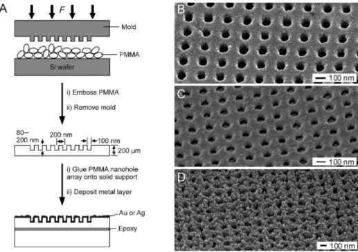
NIL is a convenient and experimentally unsophisticated technique for replicating sub-micrometer relief structures in thermoplastic polymers.32As illustrated in Figure 4A, NIL uses
a rigid mold bearing a topographic pattern which is impregnated in the polymer upon heating above its glass transition temper-ature (Tg). Cooling down below Tghardens the polymer, thereby
preserving an inverse replica of the master pattern. NIL has been shown to be effective over a broad range of length scales ranging from several millimeters to 10 nm and below. We employed this technique to fabricate metal-coated nanohole arrays in PMMA that can act as SERS-active structures with well-defined dimensions: holes had a diameter of ∼100 nm, a depth of 80-200 nm, and a pitch of 200 nm in both x and y directions. We produced PMMA sheets of about 200 µm in thickness, which are flexible enough to ensure proper release from the master. These sheets were then fixed on standard PMMA slides using epoxy glue to facilitate handling and prevent stress- or heat-induced deformation during subsequent metal deposition. SEM investigations of the metal-coated surfaces revealed that nanoscale topography did not prevent deposition of uniform and continuous films by sputtering (Figure 4B and C). ELD, in contrast, yielded arrays that are decorated with Ag deposits consisting in large part of particles that aggregated in a dense, yet irregular fashion (Figure 4D). Although the appearance of the nanohole array in Figure 4D indicates a certain degree of
alteration induced by the deposition process, the periodicity of the underlying structures remained preserved in the texture of the metal overcoat.
We conducted SERS measurements using 4-MPy as a reporter molecule to prove the suitability of metal-coated PMMA slides (Figure 5). It is generally accepted that 4-MPy chemisorbs on coinage metals via its sulfur moiety with the plane of the aromatic ring being oriented perpendicular to the surface (as illustrated in the inset to Figure 5),33 although the molecular
structure of resultant monolayers remains variable depending on the pH of the surrounding solution.34-36As can be expected,
planar areas of sputter-coated slides generally yielded no SERS response from 4-MPy molecules due to their unfavorable morphologies (data not shown). Nanohole arrays decorated with a sputtered film of Au or Ag proved suitable, however, and enabled Raman bands to be acquired, although at relatively low intensity (data not shown). SERS activity of electroless-plated Ag substrates was superior to that of sputtered films: planar regions of plated substrates yielded decent enhancements, while nanohole arrays allowed for recording Raman modes of 4-MPy37
with high intensity and resolution (Figure 5). Since the deposi-tion of the noble metals onto the nanostructured plastic substrates creates complex 3D geometries consisting of electromagnetically coupled nanoholes (top region) and nanodisks (at the bottom of each hole), the SERS enhancement is expected to be strongly influenced by the configuration of these elements.6 Shallow
arrays are very similar to continuous thin films, whereas nanoholes that are too deep will result in uncoupled pairs of disks and holes, and are equally characterized by low enhance-ment. Hence, the strongest electromagnetic enhancement is obtained when a perfect match between the wavelength of the incident laser beam and the depth of the nanoholes is achieved. Arrays comprising structures of 200 nm in depth yielded the best results within the series of substrates that were produced and inspected throughout this study.
Conclusion
In summary, we have demonstrated the possibility of fabricat-ing SERS-active substrates from hard thermoplastic materials.
Figure 4. Nanohole arrays in PMMA. (A) Schematic illustration of the fabrication process (see text for details). (B-D) SEM images of PMMA nanohole arrays coated with 20 nm of sputtered Au, 30 nm of sputtered Ag, and electroless-plated Ag, respectively.
Decoration of the surface with a thin reflective metal film can protect the plastic support during illumination with the focused laser beam and enables high-quality spectra to be acquired without notable influence by intrinsic Raman signals and background noise. Although sputtered Ag films of >20 nm in thickness proved useful to effectively shield the underlying substrate, these films were generally continuous and smooth, which is detrimental to plasmonic coupling as a prerequisite for SERS spectroscopy. ELD, on the other hand, seems suitable to produce rougher and more irregular deposits, yet the process remains to be fine-tuned so that nucleation and growth can be reproducibly controlled over nanometer length scales. Also, the development of a purely wet-chemical activation scheme that circumvents the need of any high-vacuum deposition steps would clearly add to the cost advantage provided by the plastic material and the NIL-based fabrication process. While 4-MPy served as a convenient model system for this study, future work should be directed toward label-free detection using disposable, plastic-based LOC platforms for high-throughput sensing using SERS. In principle, the transition from silicon toward plastic supports should not influence significantly the enhancement factors that are achievable using nanohole arrays (or related structures) since both materials have real indices of refraction (without any contribution from the complex part) for which the absolute values are very close to each other (e.g., ∆n ≈ 0.04 for SiO2versus PMMA).
Acknowledgment. This work was funded by the National Research Council’s Genomic and Health Initiative Program (GHI-3) and the Industrial Materials Institute. We thank our
colleagues Kien-Mun Lau, Michel Carmel, Yves Simard, He´le`ne Roberge, Nathalie Raymond, and Franc¸ois Normandin for technical assistance. We are grateful to Michel M. Dumoulin for his continuous support.
References and Notes
(1) Kneipp, K.; Kneipp, H.; Itzkan, I.; Dasari, R. R.; Feld, M. S. Chem.
ReV. 1999, 99, 2957–2975.
(2) Moskovits, M. J. Raman Spectrosc. 2005, 36, 485–496. (3) Markel, V. A.; Shalaev, V. M.; Zhang, P.; Huynh, W.; Tay, L.; Haslett, T. L.; Moskovits, M. Phys. ReV. B 1999, 59, 10903–10909.
(4) Otto, A. J. Raman Spectrosc. 2006, 37, 937–947.
(5) Alvarez-Puebla, R.; Cui, B.; Bravo-Vasquez, J.-P.; Veres, T.; Fenniri, H. J. Phys. Chem. C 2007, 111, 6720–6723.
(6) Li, K.; Clime, L.; Tay, L.; Cui, B.; Geissler, M.; Veres, T. Anal.
Chem. 2008, 80, 4945–4950.
(7) Freeman, R. G.; Grabar, K. C.; Allison, K. J.; Bright, R. M.; Davis, J. A.; Guthrie, A. P.; Hommer, M. B.; Jackson, M. A.; Smith, P. C.; Walter, D. G.; Natan, M. J. Science 1995, 267, 1629–1632.
(8) Tao, A.; Kim, F.; Hess, C.; Goldberger, J.; He, R.; Sun, Y.; Xia, Y.; Yang, P. Nano Lett. 2003, 3, 1229–1233.
(9) McLellan, J. M.; Li, Z.-Y.; Siekkinen, A. R.; Xia, Y. Nano Lett.
2007, 7, 1013–1017.
(10) Microsystem Engineering of Lab-on-a-Chip DeVices; Geschke, O., Klank, H., Telleman, P., Eds.; Wiley-VCH: Weinheim, Germany, 2004.
(11) Lab on a Chip, Daw, R., Finkelstein, J., Eds.; Nature 2006, 442, 367-418.
(12) Forrest, S. R. Nature 2004, 428, 911–918.
(13) Zhao, Z.; Peytavi, R.; Diaz-Quijada, G. A.; Picard, F. J.; Huletsky, A.; Leblanc, E.; Frenette, J.; Boivin, G.; Veres, T.; Dumoulin, M. M.; Bergeron, M. G. J. Clin. Microbiol. 2008, 46, 3752–3758.
(14) Agrawal, C. M.; Ray, R. B. J. Biomed. Mater. Res. A 2001, 55, 141–150.
(15) Lehmann, H. W.; Widmer, R.; Ebnoether, M.; Wokaun, A.; Meier, M.; Miller, S. K. J. Vac. Sci. Technol. B 1983, 1, 1207–1210.
(16) Liu, G. L.; Lee, L. P. Appl. Phys. Lett. 2005, 87, 074101-1–074101-3.
(17) Lu, Y.; Liu, G. L.; Lee, L. P. Nano Lett. 2005, 5, 5–9. (18) Jung, D.; Lee, Y. M.; Lee, Y.; Kim, N. H.; Kim, K.; Lee, J.-K. J.
Mater. Chem. 2006, 16, 3145–3149.
(19) Baia, L.; Baia, M.; Popp, J.; Astilean, S. J. Phys. Chem. B 2006,
110, 23982–23986.
(20) Bantz, K. C.; Haynes, C. L. Langmuir 2008, 24, 5862–5867. (21) Jang, S. G.; Choi, D.-G.; Heo, C.-J.; Lee, S. Y.; Yang, S.-M. AdV.
Mater. 2008, 20, 4862–4867.
(22) Willis, H. A.; Zichy, V. J. I.; Hendra, P. J. Polymer 1969, 10, 737– 746.
(23) Sears, W. M.; Hunt, J. L.; Stevens, J. R. J. Chem. Phys. 1981, 75, 1589–1598.
(24) Lee, S.-N.; Stolarski, V.; Letton, A.; Laane, J. J. Mol. Struct. 2000,
521, 19–23.
(25) Nishikida, K.; Coates, J. Infrared and Raman Analysis of Polymers. In Handbook of Plastics Analysis; Lobo, H., Bonilla, J. V., Eds.; Marcel Dekker: New York, 2003; pp 201-340.
(26) Adapted in modified form from Immunogold-SilVer Staining:
Principles, Methods and Applications; Hayat, M. A., Ed.; CRC Press: Boca Raton, FL, 1995.
(27) Schlegel, V. L.; Cotton, T. M. Anal. Chem. 1991, 63, 241–247. (28) Van Duyne, R. P.; Hulteen, J. C.; Treichel, D. A. J. Chem. Phys.
1993, 99, 2101–2115.
(29) Hecht, E. Optics, 2nd ed.; Addison-Wesley: Lebanon, IN, 1987. (30) Johnson, P. B.; Christy, R. W. Phys. ReV. B 1975, 11, 1315–1323. (31) Electroless Plating: Fundamentals and Applications; Mallory, G. O., Hajdu, J. B., Eds.; American Electroplaters and Surface Finishers Society: Orlando, FL, 1990.
(32) Guo, L. J. AdV. Mater. 2007, 19, 495–513.
(33) Sawaguchi, T.; Mizutani, F.; Taniguchi, I. Langmuir 1998, 14, 3565–3569.
(34) Jung, H. S.; Kim, K.; Kim, M. S. J. Mol. Struct. 1997, 407, 139– 147.
(35) Wan, L.-J.; Noda, H.; Hara, Y.; Osawa, M. J. Electroanal. Chem.
2000, 489, 68–75.
(36) Hu, J.; Zhao, B.; Xu, W.; Li, B.; Fan, Y. Spectrochim. Acta A 2002,
58, 2827–2834.
(37) Baldwin, J. A.; Vlcˇkova´, B.; Andrews, M. P.; Butler, I. S. Langmuir
1997, 13, 3744–3751. JP9038607
Figure 5. SERS spectra of 4-MPy taken on electroless-plated Ag/ PMMA. The spectrum in black was acquired on a nanohole array (200 nm in depth), while the spectrum in red was recorded on the planar region of the same substrate. Raman bands: 428 cm-1(C-S) in-plane
deformation/(CdC-C) out-of-plane bending; 708 cm-1(C-C) in-plane
bending/(C-S) stretch; 1008 cm-1ring stretch; 1062 cm-1(C-H)
in-plane bending; 1094 cm-1ring stretch/(C-S) stretch; 1216 cm-1(C-H)
in-plane bending; and 1576 cm-1(C-C) stretch.37