Development of Monolithic CMOS-Compatible Visible
Light Emitting Diode Arrays on Silicon
by
Kamesh Chilukuri
Bachelor of Technology in Electrical Engineering Indian Institute of Technology Madras, 2004
Submitted to the Department of Materials Science and Engineering in Partial Fulfillment of the Requirements for the Degree of
Master of Science in Materials Science and Engineering at the
Massachusetts Institute of Technology
September 2006
© 2006 Massachusetts Institute of Technology All rights reserved.
HUSETUS iNS"I
OF TECHNOLOGY
OCT 0 2 2006
LIBRARIES
Signature of Author:
Department of Materials Science and Engineering July 16, 2006
.'3
/ /-),
/
Certified by:
Merton C. Flemings-SMA Professor of Materials Science and Engineering
V
/ F ene AVFitzgerald Thesis SupervisorA
Accepted by:
Samuel M. Allen POSCO Professor of Physical Metallurgy Chair, Departmental Committee on Graduate Students
ARCHIVES
---Development of Monolithic CMOS-Compatible Visible Light
Emitting Diode Arrays on Silicon
byKamesh Chilukuri
Submitted to the Department of Materials Science and Engineering on July 16, 2006 in Partial Fulfillment of the Requirements for the Degree of Master of Science
in Materials Science and Engineering
ABSTRACT
The synergies associated with integrating Si-based CMOS ICs and III-V-material-based light-emitting devices are very exciting and such integration has been an active area of research and development for quite some time now. SiGe virtual substrate technology presents one way to integrate these materials. A more practical approach to monolithic integration based on the SiGe virtual substrate technology was followed in this work which involves wafer bonding and hydrogen-induced exfoliation to transfer a thin layer of device-quality silicon on top of the SiGe graded buffers to produce Silicon on Lattice Engineered Substrate (SOLES). SOLES wafers are suitable for the practical fabrication of SOI CMOS circuits and III-V-based photonic devices on a common silicon substrate. A novel monolithic CMOS compatible AlGalnP visible LED array on the SOLES platform was developed, fabricated and demonstrated in this work. The prototype array is an important breakthrough in the realization of the ultimate objective
-monolithically integrated optical interconnects in high speed digital systems.
Thesis Supervisor: Eugene A. Fitzgerald
Acknowledgements
I thank Prof. Fitzgerald for giving me the opportunity to work on such an exciting hands-on project.
I would also like to thank the following people:
Mike Mori for growing all the good quality AlGaInP LED heterostructures and providing PL, CL, X-TEM data.
Kenneth Lee for growing n-GaAs on n-Ge, the last AlGaInP heterostructure and for good advice on the I-Vs, L-Is and E-L spectra.
Andrew Ritenour (Antoniadis group) for tips on photomask design and suggesting some good processing recipes.
Carl Dohrman for growing the SiGe graded buffers and for collaborating on the SOLES project.
Dr. Larry Lee for growing the p++-Si/p -GaAs heterojunction. Bai Yu for growing the p÷÷-Ge/p -GaAs heterojunction. Jason Orcutt (Ram Group) for the L-I curves and EL spectra. Jennifer Yu (Bulovic group) for EL spectra.
Dr. Mayank Bulsara for photomask design tips and good general advice. MTL staff for training me on the ICL/ TRL equipment.
TABLE OF CONTENTS
A bstract ... 3
A cknow ledgem ents ... 5
Table of Contents...7
List of Figures ... .. 9
CHAPTER 1:Introduction ... 11
1.1 Introduction and Scope of the thesis ... ... 11
1.2 Board Level (Chip to Chip) Optical Interconnects ... 12
1.3 Latency, Power and Bandwidth Comparison... 13
1.4 Optical Interconnects in Monoprocessor and Symmetric Multiprocessor machines ... ... ... ... ... 1... 15
1.5 Optical Interconnects in dedicated processors ... ... 16
CHAPTER 2:Development of the SOLES Integration Platform ... 18
2.1 Introduction ... ... ... 18
2.2 Monolithic Integration via the SiGe Graded Buffer ... 18
2.3 Silicon on Lattice Engineered Substrate(SOLES) ... 20
2.4 Fabrication of SO LES ... ... 21
2.5 R esults ... 25
CHAPTER 3:Development of CMOS-Compatible Contact Technology for III-V LED s ... 28
3.1 Introduction ... 28
3.2 The n-GaAs / n-Ge heterojunction... 29
3.2.1 Interdiffusion at the GaAs/Ge interface ... 29
3.2.2 Material characterization -SIMS Analysis... 29
3.2.3 Electrical characterization - Mesa diode fabrication ... 32
3.2.4 Electrical characterization - Results and Discussion... 34
3.3 The p÷+-Si /p÷-GaAs heterojunction ... ... ... 38
3.3.1 Material characterization -SIMS Analysis ... 38
3.3.2 Electrical characterization - Mesa diode Fabrication ... 39
3.3.3 Electrical characterization - Results and Discussion... 40
3.4 The p÷÷-Ge/p÷-GaAs heterojunction ... ... 42
3.5 CMOS-compatible ohmic contacts to Ge ... ... 44
CHAPTER 4:Design and Fabrication of AlGaInP Visible Light Emitting Diodes.. 47
4 .1 Introduction ... 47
4.2 The (AI)GaInP material system ... 47
4.3 Double-Heterojunction (DH) AlGaInP LED design... ... 48
4.3.1 Active Layer Design ... 50
4.3.3 Current spreading layer design ... ... 52
4.3.4 Encapsulation layer design ... 53
4.4 A lG alnP G row th Issues ... ... 53
4.5 Effect of the p++-Si encapsulation layer... ... 54
4.6 p+*-Si encapsulated AlGaInP LED on SiGe graded buffers ... ... 57
CHAPTER 5:Design and Fabrication of Monolithic CMOS-Compatible Visible LED Arrays on Silicon ... 64
5.1 Introdu ction ... 64
5.2 Two Dimensional LED arrays ... 64
5.3 LED Array Photomask Design ... 65
5.3.1 LED Array Mask Layout ... 66
5.3.2 Alignment Mark design ... 69
5.4 LED A rray fabrication ... ... 70
5.5 R esults and D iscussion ... 74
CHAPTER 6:Conclusions and Future Work ... ... 79
6.1 Summary of accomplishments... .... 79
6.2 Suggestions for future work... 80
APPENDIX Al...82 APPENDIX A2...83 APPENDIX A3...85 APPENDIX A4...87 APPENDIX B...91 APPENDIX C...97 APPENDIX D... 100 BIBLIOGRAPHY ... 102
LIST OF FIGURES
Figure 1.1: Partition length vs. technology generation. [2] ... . 14
Figure 2.1: (a) Schematic of compositionally graded buffer. (b) Cross-sectional transmission electron micrograph (TEM) of a compositionally graded SiGe region showing recycling of threading dislocations. Image courtesy Thomas Langdo ... 19
Figure 2.2:Cross-sectional TEM image of Ge capped SixGel-• graded buffer grown in the Fitzgerald group UHVCVD reactor ... ... ... 20
Figure 2.3: A III-V/SiGe mesa etched to reveal the underlying Si substrate creates a 12[tm step between electronic devices and III-V material... ... 21
Figure 2.4: Schematic showing practical monolithic integration using the SOLES wafer. ... 2 1 Figure 2.5: Schematic of the Strasbaugh 6EC laboratory polishing system. Courtesy A rthur Pitera ... 23
Figure 2.6: Infrared camera image of oxide-coated SiGe handle wafer bonded to a Si donor wafer. ... 24
Figure 2.7: The SOLES fabrication process sequence... ... 26
Figure 2.8:Cross-sectional TEM image of the fabricated SOLES wafer. Courtesy Carl D ohrm an ... 27
Figure 3.1: Schematic of the CMOS compatible III-V LED ... 28
Figure 3.2: Semilog SIMS concentration profile for Ga, As and Ge atoms ... 30
Figure 3.3:Semilog plot of the concentration profiles of As and Ga obtained by backside SIM S ... 31
Figure 3.4: Plot of Ga and As concentration vs. depth on a linear scale obtained by backside SIM S ... 32
Figure 3.5: Schematic showing the GaAs/Ge mesa diode fabrication sequence ... 33
Figure 3.6: Photomicrograph of the fabricated GaAs/Ge mesa diode. The mesa size is 200 lmx200ýtm and the contact pad size is 75,tmx75tm ... 35
Figure 3.7: Semi- log I-V characteristic of the GaAs/Ge diode of Figure 3.6. The Ge contact was grounded and bias on the GaAs contact was swept from negative to positive. ... 3 5 Figure 3.8: Band lineup for the n-Ge/ n+-GaAs heterojunction ... 36
Figure 3.9: The n-p-n diode structure and the equivalent electrical circuit ... 37
Figure 3.10: SIMS profile of Ga, As and B species in the p"+-Si/p+-GaAs stack... 39
Figure 3.11: Schematic of the p++-Si/ p÷-GaAs mesa diode. ... 40
Figure 3.12: I-V characteristic for the p++-Si/ p+-GaAs diode ... 41
Figure 3.13: Band lineup for p-Si /p-GaAs material system. ... 41
Figure 3.14: Schematic explaining the carrier tunneling theory for heavily doped Si/GaAs junction. ... 42
Figure 3.15: SIMS profile of the B, Zn concentrations in the p++-Ge/p+-GaAs stack... 43
Figure 3.16: I-V characteristic of the p+-Ge/p+-GaAs heterojunction ... 44
Figure 3.18: I-V characteristic of TiGe contacted Ge. Ti/Al was annealed in forming gas ambient at 400 TC for 40min to form TiGe ... 46
Figure 4.1: The energy gap of the AlGaInP alloy vs. lattice constant [12]. ... 48
Figure 4.2 (a): The DH LED stack (b): Schematic of the free carrier distribution in a Double Heterojunction under forward bias... 49
Figure 4.3: (a) Schematic of LED mesa diode structure without Si cap. (b) with Si cap. 55 Figure 4.4: (a) Device with no Si cap -peak at 649nm and FWHM = 25nm (b) Device with Si cap - peak at 654nm and FWHM =24nm. ... ... 55 Figure 4.5: Photomicrograph of an AlGalnP LED grown on semi-insulating GaAs
substrate biased at 30m A .... 56 Figure 4.6:Semilog I-V curves for AlGaInP LED on GaAs substrate with and without Si
c ap ... 5 6
Figure 4.7: Fiber coupled power vs. bias current for devices with and without Si cap.... 57 Figure 4.8: Cross-sectional TEM image of the LED layers grown on the graded buffer substrate. The Si cap was grown in-situ in the MOCVD reactor. Image courtesy Mike
M ori... 58
Figure 4.9: Spectral response of Si-capped LEDs on bulk Ge and SiGe graded buffer
substrate at 30m A bias. ... 59 Figure 4.10: Semi-log I-V plot of p+-Si capped LED on SiGe buffers and bulk Ge
substrates ... ... 60 Figure 4.11: L-I curves of pf+-Si capped LED on SiGe buffers and bulk Ge substrates. 61
Figure 4.12: SIMS data for P++-Si capped LED stack on SiGe graded buffer substrate.. 62 Figure 4.13: SIMS data for P++- Si capped LED stack on SiGe graded buffers showing the
B and Zn concentrations. ... 63 Figure 5.1: Schematic showing the concept of junction isolation to prevent cross-talk
betw een pixels... 65 Figure 5.2: Schematic of the Photomasks. Levels Polystrip, Metal 1 and Metal 2 are bright field while Active, Isolation trench, LED well, Via 1 and Via 2 are dark field... 66
Figure 5.3 : Photom ask layout for a 2" wafer ... 67 Figure 5.4: Layout of the die showing different LED arrays, the TLM and mesa diode
structures and alignment marks. ... 68 Figure 5.5: A pixel in the 100x100 central LED array -plan and cross-section views.... 68 Figure 5.6: Nomarski image showing single crystal material in (a) 36 [tmx36 gim growth wells (poly-etch mask size will be 22=mx22jim). (b) 122 [tmx 122[tm growth wells (poly-etch mask size will be 102[tmxl02[tm) of a portion of the central LED array... 72 Figure 5.7: 20 gimx20 gtm LED; 3 gim critical dimensions;Array pitch =40 gtm (- 600dpi) driven at 50mA current. The contact pads are 100 jtmxl00 jtm squares... 75 Figure 5.8: (a) Unbiased LED array. (b) Top LED pair at 50mA bias (c) Bottom row at
50mA bias. In (b) and (c) all ambient light sources have been turned off... 75 Figure: 5.9 A pixel in the central 100x100 array biased at 50mA ... 76 Figure 5.10: Spectral response at 50mA bias of a typical pixel in the central array ... 76 Figure 5.11: Cross-sectional TEM image of the material grown in a typical oxide well of
the central 100x100 array. Courtesy Mike Mori ... ... 77 Figure 5.12: I-V characteristic of a typical pixel in the central 100x100 array. ... 78 Figure 5.13: L-I curve for a typical pixel in the central 100 x 100 array... 78
CHAPTER 1
Introduction
1.1 Introduction and Scope of the thesis
Silicon (Si) has the advantage of well-developed process and design technologies, availability of large size, high quality, inexpensive substrates, and a stable native oxide suitable for dielectric passivation. All these features have contributed to silicon ICs dominating the electronics industry for the past four decades. Silicon, however, is an indirect bandgap semiconductor incapable of emitting light by conventional methods. The invention of III-V compound-based light-emitting devices in the 1960's ushered in a bright new era for the semiconductor industry. The possible synergies that can be developed by integrating Si-based ICs with III-V-compound-based light-emitting devices are very exciting and such integration has been an active area of research and development for quite some time now.
There are two general categories of optoelectronic integration, hybrid and monolithic. Whereas hybrid integration involves the alignment and mounting of pre-fabricated II-V components on a host Si IC, monolithic integration utilizes a common semiconductor substrate on which both optical and electrical devices are built. Monolithic integration has the advantage of economies of scale compared to hybrid integration which is labor intensive and volume-limited.
Though monolithic integration sounds attractive it is not easy. First, the lattice mismatch between Si and III-V compounds like GaAs makes the direct growth of good quality GaAs on Si impossible. One alternative to obtain low defect density GaAs on silicon is to use compositionally graded SiGe buffer layers to bridge the gap between Si and GaAs lattice constants (i.e., creating a virtual SiGe substrate, closely lattice-matched to GaAs). Though in theory the SiGe layers can be etched in selective areas to reveal the underlying silicon for CMOS circuit fabrication, the resulting 10 CPm step makes high resolution lithography on this substrate difficult. Second, III-V materials traditionally use gold-based contact metallurgies. Gold is considered unsuitable for silicon electronic devices since it introduces deep level traps in the Si energy bandgap that deteriorate
device performance. Third, the introduction of III-V materials in Si fabrication facilities could compromise the standard CMOS process.
The aim of this work is to successfully integrate Si and III-V material by overcoming the above barriers. This is realized through the development of a CMOS-compatible visible light-emitting diode (LED) array on silicon. Chapter 2 presents the work done to develop a novel substrate called Silicon on Lattice Engineered Substrate (SOLES) that enables practical monolithic integration. For CMOS compatibility, the electrical properties of the n-GaAs/n-Ge, p++-Si/p+-GaAs and p÷+-Ge/p+-GaAs junctions are studied in Chapter 3. The design, fabrication and characterization of silicon-encapsulated AlGalnP LEDs on bulk GaAs and SiGe virtual substrates is described in Chapter 4. The LEDs are finally integrated on SOLES to make the prototype LED array as discussed in Chapter 5. Chapter 6 concludes the thesis and gives direction for future work.
The prototype LED array developed in this work is an important milestone towards achieving the ultimate objective - monolithically integrated optical interconnects inside digital systems. Before proceeding with the practical aspects of this work, a technology evaluation of board level optical interconnects is presented in the following, in order to identify useful applications.
1.2 Board Level (Chip to Chip) Optical Interconnects
For long distance communication links the use of optical signaling has been preferred to electric signaling because of lower attenuation for optical signals. These optical links employ serial communication in which the data bits are sent over a single communication channel (typically optical fiber) in a serial fashion one after the other.
However, using light for communication within the computer system is markedly different because attenuation over such short link lengths is not of major consequence. Rather the issues are latency, power consumption and bandwidth. Latency considerations favor board level (chip to chip) communication being parallel as opposed to serial. Though multi-channel electrical interconnects have so far been satisfactory, optical interconnects with low timing skew (important for parallel communication), low crosstalk and high bandwidth seem to be promising. A comparison of electrical and optical interconnects is performed in the next section.
1.3 Latency, Power and Bandwidth Comparison
The latency in an optical interconnect link is due to the latency associated with the laser driver and laser-diode at the transmission side and with the photo-diode, trans-impedance amplifier (TIA), signal level restorer at the receiver end, besides the time of flight (ToF) latency which is dictated by the speed of light.
Bitzaros et al. [1] found that for optical link lengths in the few-centimeter range latency is dominated by the interface circuits since the ToF latency is negligible for such short lengths. At board level lengths (10 cm) the ToF latency dominates the link latency of optical interconnects. For electrical interconnects, relatively wide and thick wires available at the board level can result in latencies close to ToF. Thus, optical and electrical interconnects can have comparable latencies at the board level.
"Optoelectronic links can be superior to electrical links in terms of power dissipation in highly parallel interconnections. When multiple channels of optoelectronic links are considered, the biasing circuitries of the TIA and laser driver can be common for all channels. As a result, in multiple-channel optoelectronic links, the total power consumption is not a direct multiple of the single-channel consumption, as is the case with electrical interconnects. Therefore, the optoelectronic links can be more efficient than electrical interconnects in multi-channel links"[1]. However, reducing the voltage swing of electrical interconnects can make the energy dissipation of electrical and optical interconnects comparable [2].
Though latency and power consumption do not provide any great advantage to favor the use of optical interconnects at the board level, the substantially large bandwidth is a factor in their favor. According to Naeemi et al. "While bandwidth of an electrical interconnect is determined by its length and cross-sectional dimensions, the bandwidth of a typical board level waveguide is independent of its physical dimensions, and is determined by the driver and receiver. To have a fair comparison between electrical and optical interconnects, bandwidth and interconnect density should be considered simultaneously. This means that data flux density (defined as bandwidth per unit width of interconnect) should be compared. A large data flux density is desirable so as to transfer as many bits per second as possible using a constant routing area." [2].
Naeemi et al. [2] identify a partition length beyond which optical waveguides can
offer a larger data flux density or larger aggregate inter-chip bandwidth in comparison to electrical interconnects when constrained by a fixed routing area. In their analysis, it is assumed that optical drivers and receivers will eventually mature and become comparable with their electrical counterparts in terms of power, size, and cost. Their comparison, therefore, emphasizes the interconnect media, or "wires versus waveguides," rather than the interface circuits.
Figure 1.1 plots the partition length for different technology nodes. As technology advances, the partition length decreases, because of reduction in linewidth and increase in operating frequency. It is seen that the partition length is expected to reduce to 10 cm by the year 2008, indicating that optical interconnects will then provide a higher bandwidth flux than electrical interconnects at the board level.
141
120
10
jlO
IA
Figure length1.1 Partition Figure 1.1 Partition length
M04 267 3I1O 2013
Year
96 645 32
Technology Generation (nm)
vs. technology generation. [2]
In summary, comparison of electrical and optical interconnects has shown that optical interconnect technology is attractive at the board level due to its capability of
2016
sustaining a high bandwidth density. Signal latency and power consumption are not compelling factors in favor of optical interconnects.
1.4 Optical Interconnects in Monoprocessor and Symmetric Multiprocessor machines
Though optical interconnects have revolutionized telecommunications they have hardly found applications within computer systems. According to Collete et al.[3] the reason is that optics does not shorten the access time to the memory (Memory Access Latency, MAL), which is the most crucial issue for stored-program machines. Latency is the critical factor when considering the interactions between the memory and the processor, more than bandwidth, because the processor exchanges very short bursts of information with the memory.
Collete et al. argue that "the performance of microprocessors has increased much more rapidly than that of memory systems. Processor speeds have doubled every few years, while the speed of dynamic random access memory (DRAM) has increased only marginally. This means that the time needed by the processor to fetch instructions or data from the main memory has increased compared with the processor cycle time. The speed of DRAM is limited by the circuits used for detecting the stored charge on a memory cell. There is a trade-off between the size of the memory and the rate at which the stored charge can be sensed. In monoprocessor machines the dominant term to the MAL is the intrinsic MAL, which depends on the internal architecture and on the technology of the DRAM. Thus the high bandwidth provided by optical interconnects cannot help improve the performance of monoprocessor machines."[3]
"In order to enhance computer performance several processors can be connected through an interconnection network. In such multiprocessor machines, the additional terms of coherence latency and contention latency contribute to the MAL. In order to maintain the coherence of the caches, coherence messages need to be broadcast through the communication network. This slows down the memory access and adds coherence latency to the MAL. Coherence latency strongly depends on the network topology. Snooping protocols for maintaining cache coherence, usually implemented with bus topology, are much simpler and faster than directory-based protocols that have to be implemented in distributed networks."[3].
"In symmetric multiprocessor designs a single address bus is shared (this enables snooping to maintain cache coherence) among the processors and memory controllers. If the address bus is busy when a processor needs data, that processor must wait for its turn, causing contention latency. Therefore, there is only a marginal improvement when more processors or faster processors are added to a system without increasing the address bus bandwidth. Increasing the bus operation frequency is complicated because the bus being
used is a multipoint electric line."
"High bandwidth optical interconnects offer an alternative solution. Address bus speed can be increased using optical interconnects without the effects of crosstalk, impedance mismatch and signal degradation encountered in electrical solutions. Parallel transmission through optical lines is almost skew-free in the gigahertz domain for transmission over a few tens of centimeters thus simplifying data recovery. However there are limitations to the use of optical interconnects. Increasing the bus operating frequency will also require each cache controller to check and update its directory at the bus operation frequency. Speeding up the bus will also generate a physical integration issue because the bus length has to be limited to make sure that the optical signals can be stationary within a single bus period. The light propagation velocity (c = 20 cm/ns) requires the bus to be shorter than 10 cm at 2 GHz, shorter than 5 cm at 4 GHz, etc."[3]. Thus optical buses do not seem to be a solution to the MAL in symmetric multi-processor machines. New computer architectures will have to be developed to attain any benefit.
1.5 Optical Interconnects in dedicated processors
The most viable application of optical interconnects at present seems to be in dedicated optoelectronic processors. Collete et al. declare that "Dedicated processors do not generally execute stored programs unlike general purpose monoprocessors or multiprocessors. They are designed for a specific task, involving the processing of optical information. The MAL is no longer a problem as there is no memory or almost no exchange with the memory. Some examples of applications for dedicated processors are image-processing-primitive operations (Fourier transformation, 2-D convolution and correlation, and dot-product and dot-matrix multiplications)" [3].
In summary, optical interconnects can provide huge bandwidth. But this cannot be exploited in monoprocessor machines. In multiprocessor machines, a high bandwidth will
decrease the MAL but a new computer architecture has to be employed to attain this benefit. Thus within the constraints of the present architecture the most promising applications of optical interconnects seem to be in dedicated microprocessors.
CHAPTER 2
Development of the SOLES Integration Platform
2.1 Introduction
In order to implement optical interconnects in digital systems, optoelectronic integrated circuits (OEICs) must be developed. OEICs depend on the integration of electrical devices such as transistors which are typically fabricated in silicon and optical devices that are fabricated in compound semiconductors such as GaAs. This integration can be achieved by monolithic or hybrid means. Commercial devices till date have relied upon costly hybrid mounting schemes. Historically monolithic integration has been attempted via the epitaxial growth of GaAs directly on Si, but the nearly 4% lattice mismatch between Si and GaAs results in defect densities on the order of 1010 cm-2 in the GaAs epilayers, rendering the material useless for device applications.
2.2 Monolithic Integration via the SiGe Graded Buffer
Monolithic integration requires growth of low defect density III-V material on a Si substrate. SixGel.x alloys present one way to bridge the lattice mismatch between Si and GaAs by acting as a template for lattice matched GaAs growth. The lattice parameter of the SixGel_x alloy can be engineered by varying the composition 'x' of the alloy from 1 to 0 thereby starting with 100% Si at the bottom and obtaining 100% Ge on top. The resulting Ge cap is closely lattice matched to GaAs.
However, the Ge cap obtained by this method is not defect-free. As the thickness of a mismatched film increases, the misfit strain energy stored in the film increases. At a certain film thickness, termed the critical thickness, misfit dislocations are nucleated to relieve the strain associated with lattice mismatch. Dislocations must terminate outside the epitaxial film so the dislocations have to either terminate at the wafer edge or on the film surface. Those dislocations that end on the film surface have to "thread" through the film thickness and hence are termed threading dislocations. Figure 2.1(a) shows misfit and threading dislocations. High densities of threading dislocations (1010 cm-2) can seriously degrade the efficiency of a semiconductor device by acting as non-radiative recombination centers for electrons and holes.
One way to control the threading dislocation density in the SiGe graded buffer to the desired order of 106
cm-2 is to reduce their nucleation. This is achieved by maintaining a low strain state during growth. Thus, the highly mismatched Ge target layer is approached gradually via the deposition of many intermediate layers of low lattice mismatch. Each layer in the buffer relaxes to its intermediate lattice constant, and a low strain state is maintained throughout, minimizing dislocation nucleation. Additionally, threading dislocations from previous layers are "recycled" at each subsequent interface as they glide to create misfit dislocations. A high growth temperature is employed to maximize the glide length of each threading dislocation at each interface, obviating the need for additional dislocation nucleation for strain relief. Figure 2.1(b) illustrates the recycling of threading dislocations in the graded buffer.
Si substrate
(a) (b)
Figure 2.1: (a) Schematic of compositionally graded buffer. (b) Cross-sectional transmission electron micrograph (TEM) of a compositionally graded SiGe region showing recycling of threading dislocations. Image courtesy Thomas Langdo.
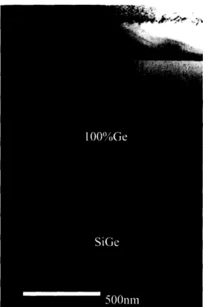
A cross-sectional transmission electron microscope (TEM) image of a SiGe graded buffer on Si with a 1 [tm Ge cap suitable for III-V integration is shown in Figure 2.2. The batch process nature of the ultra high vacuum chemical vapor deposition (UHVCVD) system permits high-quality Ge/SiGe/Si graded buffer growths on multiple 4" or 6" Si substrates with grading rates of 10% Ge per gjm and growth temperatures between 550 'C-800 'C.
1
im
Figure 2.2:Cross-sectional TEM image of Ge capped SixGelx graded buffer grown in the Fitzgerald group UHVCVD reactor.
2.3 Silicon on Lattice Engineered Substrate (SOLES)
Though the SiGe graded buffer can bring GaAs and Si to the same wafer, it is not a practical way for achieving monolithic integration. A grading rate of 10% Ge per jim for the SiGe buffer will result in a graded buffer thickness of 10gm. Capped with 1 jim Ge and assuming a 1 gm III-V layer, a total thickness of 12 gm is obtained.
Though in theory a III-V/SiGe mesa can be etched to access the underlying silicon for transistor fabrication as shown in Figure 2.3, in practice a 12 gm mesa will introduce nonplanarity which will negatively impact the lithography resolution. To achieve high resolution, the wafer has to be planarized but this involves deposition of very thick oxide (about 3 times the step height) and a chemical-mechanical polish step.
12jim 1i1-V
SiGe
Figure 2.3: A III-V/SiGe mesa etched to reveal the underlying Si substrate creates a 12pm step between electronic devices and III-V material.
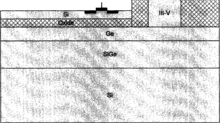
One way to overcome this drawback is to add a device-quality silicon layer on top of the SiGe buffer using intervening oxide layers, thereby reducing the step height between Si and III-V material to 0.5gm or less and making the integration process more tractable (Figure 2.4). This approach was adopted to demonstrate monolithic integration in this work. The next section details the fabrication process used to make this platform.
Figure 2.4: Schematic showing practical monolithic integration using the SOLES wafer.
2.4 Fabrication of SOLES
The process used to fabricate the structure shown in Figure 2.4 (Silicon on Lattice Engineered Substrate, also called SOLES) is essentially a modified version of the SMART-CUT® process [4]. The key steps in this process are hydrogen implantation, low temperature oxide growth, chemical mechanical polishing, wafer bonding and annealing to cause hydrogen-induced exfoliation and transfer of the silicon layer. In the traditional
i-
-Si"
•
•.
.:
•
.:
:
.:..
.
..
.
..
...
:
..
...
•..•...:
..
,...ii..
:
..
.:.
.
..
."
:
.
:
...
....
:
.:
:
••
.
:.i.:
:
,.,:.i.
.i.:
••"
..:.
'
Ge SIGe
Si
,, ::,:, :::", ,:: " ks •!,i::':••:::•:: :!,, !!!• · ::- ,:,:i ::,,!ii:, ,,, ;; :: ::•- : :::::,•i,::i: :,;, :•, :,•i i•,•.•' •i!!• ,,•:? ::•!!•i , :! i:ii: : i• ,i!·!ii!i:!:•,:: i,• • i ::•::i•,,i,•' ' : ,:,,i:;::: '•,:• :,::i:~,,,::,,::,•,::i:,:, i , ,,•:# ," ,: ,i;: !•:: •i:• :::,!::!i:: ,:•i,•li :::!• :!·i:i", ,:i:,," i -ii::::,~ :•!',•::i::::• ::i i:,::: •: :•' ,: i,, ,,::: ::
•.. : :... :.: :.:...: : .: ... " :. !... ..:..."...- ::..:.... :: :. ;•J .:::.. :: !Y :.: :::: • • • .!i : • . i ": .•i• .;! .••. . .. i : : :::i.:••::: !. ' • i • .: ) ::? ::.:•..• .: i:•? • :• i:::! ..:.::.::!..:i ': .
SMART-CUT® process, silicon is bonded to silicon dioxide whereas in the modified process, oxide-to-oxide bonding occurs. Since the graded buffer surface is unusually rough and is marked by a representative crosshatch pattern, oxide layers are used to make the surfaces smooth for bonding. Besides facilitating bonding, the silicon dioxide layer isolates the thin Si film from the underlying Ge layer, thus preventing crosstalk between the CMOS driver and III-V optical devices.
The starting materials in the process are a 6" SiGe virtual substrate (henceforth called the handle wafer) and a 6" Si prime wafer (henceforth called the donor wafer because it donates the thin Si layer to the handle wafer).The first step is wafer cleaning prior to growth of the oxide layer. The donor wafer was cleaned using the standard RCA clean and a 200
A
thin layer of thermal SiO2 was grown. The donor wafers were then sent to an external vendor for hydrogen ion implantation. (Dose = 5x1016 cm-2, Implant energy= 80 KeV, Tilt = 7°). These implant conditions create a hydrogen-rich layer at a depth of about 0.3 ýtm from the surface.
The standard RCA clean could not be used for cleaning the handle wafer since hydrogen peroxide (H202) attacks Ge. Therefore the handle wafers were cleaned using a modified RCA clean that has a reduced exposure time to H202. The modified RCA clean recipe is given in Appendix C. A 7500
A
thick low temperature oxide (LTO) at 400 TC was next deposited on the handle wafers. The LTO deposition ensured that there was no temperature-related damage to the Ge virtual substrate. However, LTO films suffer from two drawbacks - one, they contain significant amounts of residual hydrogen from the deposition process which can lead to pockets of trapped gas at the bonded interface during wafer bond annealing, causing the bond to fail. Second, their surface roughness is too high for bonding. The first problem was overcome by annealing the wafers at 650 TC for 2 hours to expel the trapped gas and densify the oxide layer. The second hurdle was overcome by chemical-mechanical polishing (CMP). A brief description of the CMP process follows.A Strasbaugh 6EC laboratory polisher (Figure 2.5) was used to reduce the roughness of the handle wafers to levels acceptable for bonding. The setup consists of a 22" polishing table with a Rohm and Haas IC1000 layered CMP pad. The pad is conditioned with a diamond-grit disc that lifts the nap of the CMP pad during wafer
polishing, thereby maintaining a constant material removal rate. Cabot's Semisperse-25 fumed silica slurry, diluted (1:1) with deionized water (DI) was used for polishing the LTO film. The wafer is held in place in the quill that rotates in the same direction as the polishing table. The downforce (Pd) is applied by a hydraulic piston to the entire wafer carrier, thereby setting the contact pressure between the wafer and the CMP pad. The backpressure (Pb) is a pneumatic pressure applied to the back of the wafer to maintain polish rate uniformity across the wafer surface.
Pad cnnditinner
Figure 2.5: Schematic of the Strasbaugh 6EC laboratory polishing system. Courtesy Arthur Pitera.
The chemical component of oxide CMP is water, which serves to weaken the oxide bonds by the hydrolysis reaction given by
(SiO2)x + 2H2 0 - (SiO2) x- + Si(OH)4 Equation 2.1
This reaction is accelerated by the compressive stress induced by the interaction of the CMP pad and slurry particles with the wafer surface. The reaction products are subsequently removed by the additional mechanical action of slurry particles. As a result, both chemical and mechanical removal mechanisms are enhanced at surface asperities leading to high planarization efficiency.
The material removal rate by CMP for the parameters of the recipe given in Appendix C was determined as - 20A/s. The wafers were polished for 250 seconds to remove about 5000 A of oxide. After polishing, the wafers were immediately cleaned with a polyvinyl sponge and rinsed with DI water to remove the slurry deposits and
transported immersed in DI water to the piranha acid hood to prevent any residual slurry from drying on the surface. If the slurry dries, chemical bonds are formed between the particulates in the slurry and the wafer surface making it hard to remove. The wafers were piranha cleaned and spin-rinse dried using the recipe given in Appendix C. A similar CMP step for the donor wafers was not required since the thermal oxide on the donor wafers is smooth enough for bonding.
The next step involves bonding the donor and handle wafers. Before bonding, it is necessary to clean the donor and handle wafers to make the surfaces hydrophilic. A modified RCA clean (only SC1, no SC2 or HF dip) was used for this purpose. Once cleaned, the wafers were aligned and placed in a bonding chuck using the EV620 wafer aligner, transferred to the EV501 wafer bonder, and bonded. The wafer bonder performs two primary functions. Flags are used to keep the wafers separated at the edges until contact is initiated at the center of the two wafers. It also allows the application of force by applying pressure via a pressure chamber. The wafers were removed from the bonder and inspected with an IR camera. A picture of the bonded wafers is shown in Figure 2.6.
L
A
Figure 2.6: Infrared camera image of oxide-coated SiGe handle wafer bonded to a Si donor wafer.
Although the room temperature bond is strong enough to permit handling of the wafers, it is necessary to anneal the wafers to enable the oxide layers to fuse together and form stronger bonds. The wafers were furnace annealed at 250 oC for 1 hour for this purpose. While in the furnace, the temperature was ramped up to 450 OC and held for 1 hour to cause hydrogen-induced exfoliation and Si layer transfer. A schematic of the
fabrication process flow is shown in Figure 2.7.
2.5 Results
The Si layer transfer was successful and was uniform across the 6" SiGe virtual substrate. A cross sectional TEM image of the fabricated SOLES wafer is shown in Figure 2.8. Exfoliation-related damage can be seen in the top regions of the transferred Si layer. For device fabrication, the damaged silicon can be removed either by a touch polishing step as in the SMARTCUT® process or by a timed wet/dry etch.
In summary, the SOLES material platform was successfully fabricated by wafer bonding and annealing to cause hydrogen-induced exfoliation and transfer of a thin device quality silicon layer on top of the graded buffer substrate. The fabricated SOLES wafer will be used to demonstrate practical monolithic integration.
Handle Wafer : 6 inch graded buffer
Thermal oxidation Low Temperature Oxide(LTO)Deposition
SiGo+. .'
• ~~.:: :: :•:i:.•_:•:.. . ....:: i. .s • " "• " " •: • •::( :: :!:ii:ii
• : .. .. :. . , : . ._ .. . . . ,. . .
• ". • .;..:i;.:;: ~· .•;".• :.;....:• :..• . . . . . . ., . . .:i. ... .. " . . .: ':; ).·..;:·::. . .
CMP front side LTO
SiGe . . . .... . . BONDED INTERFACE BOND ~~...2 222222ttANVV·.VC : 1 : ::: Ste. Anneal
Figure 2.7: The SOLES fabrication process sequence.
H* H* H* H+ H* H' H* HV
SiGe Donor Wafer 6 inch silicon
Figure 2.8:Cross-sectional TEM image of the fabricated SOLES wafer. Courtesy Carl Dohrman
CHAPTER 3
Development of CMOS-Compatible Contact Technology for
III-V LEDs
3.1 Introduction
Following the successful fabrication of SOLES substrates suitable for practical monolithic integration, III-V materials must be introduced into a commercial Si CMOS fabrication facility without compromising the standard CMOS process. Such an introduction requires that the III-V material is not etched or exposed during processing in CMOS compatible tools. Also, the conventional gold-based ohmic contact metallurgy for III-V compounds/Ge cannot be used since gold forms deep level traps within the bandgap of silicon.
CMOS compatibility as outlined above was achieved in this work by accessing the n-GaAs cathode of the LED through the underlying n-Ge layer rather than etching through the III-V material of the LED stack. Further, encapsulating the LED with a thin film of CMOS-compatible material (like Si) prevents the exposure of III-V material while processing in CMOS compatible tools. Figure 3.1 shows a schematic of an LED structure employing this contacting scheme.
CMOS Compatible
Contact Metallurgy
Using such a scheme introduces an n-GaAs/n-Ge and p-Si/p-GaAs heterojunction in series with the LED stack. For a given current, the extra voltage drop across these junctions will increase the joule heating of the device thereby degrading its efficiency. It is therefore important to understand the contribution of these heterojunctions to the overall voltage drop between the anode and cathode metal contacts of the LED.
3.2 The n-GaAs / n-Ge heterojunction
To understand the properties of the n-GaAs/n-Ge heterojunction, 1 gim nominally undoped GaAs was grown by MOCVD on epi-ready double-side polished two inch n-type Ge substrates (Sb doped, resistivity = 0.1 ohm-cm) misoriented 60 towards <111>. GaAs growth was undertaken at a high temperature (650 oC) and with a high ratio of AsH3 to (CH3)3Ga source gas flow rates in order to eliminate antiphase boundaries (APBs). APBs can serve as large-scale trapping sites to reduce minority carrier lifetime in GaAs device layers and also act to increase majority-carrier scattering in electronic circuits [5].
3.2.1 Interdiffusion at the GaAs/Ge interface
A difficulty with GaAs on Ge epitaxy is the interdiffusion of atoms at the GaAs/Ge junction. Whereas Ga and As can move down into the Ge substrate via solid state diffusion during growth, doping the Ge p- and n- type respectively, Ge atoms mainly contaminate GaAs epilayers through vapor phase transport during the deposition process, doping it n-type.
Ge out-diffusion can counter-dope p-type epi-layers, thus reducing device efficiency. This problem can be overcome by limiting the vapor phase transport of Ge during MOCVD growth [6]. It has not been possible to reduce Ga and As diffusion into the Ge substrate since the conditions that eliminate APB formation (high temperature and high AsH3 to (CH3)3Ga ratio) cause significant solid state diffusion of these species [7].
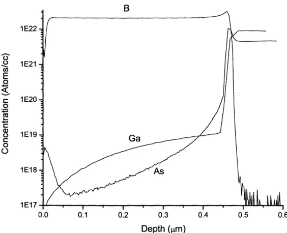
3.2.2 Material characterization -SIMS Analysis
Interdiffusion at the GaAs/Ge heterointerface was investigated by secondary ion mass spectroscopy (SIMS). SIMS is a powerful tool for the quantitative measurement of dopant and impurity levels in semiconductors. The technique relies on bombardment of the sample surface with a primary ion beam followed by mass spectrometry of the
emitted secondary ions [8]. For the GaAs on Ge sample in this work, Cs+ primary ions were accelerated to an energy of 2 keV and the mass spectral peak intensity of the emitted ions was analyzed. The resulting concentration profile is shown in the semi-log SIMS plot of Figure 3.2. Note that zero on the x-axis corresponds to the GaAs surface and the GaAs/Ge interface is at a depth of approximately 1000 A from the surface.
Ge 1E22 o' 1E21 o E 0 3 1E20 c-O c 1E19 0 0 1E18 1E17 0
Figure 3.2: Semilog SIMS
500 1000 1500 2000 2500
Depth (A)
concentration profile for Ga, As and Ge atoms.
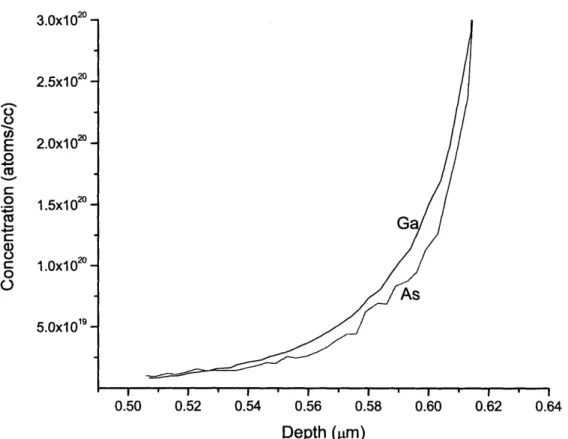
It is seen that Ge heavily autodopes GaAs epilayers greater than 1020 cm-3 throughout the film. The SIMS profile of Figure 3.2 is accurate only for the Ge concentration. The long As tail in Ge near the interface is an artifact of SIMS called the "knock in" effect wherein the high energy primary ions knock the Ga and As atoms from GaAs into the Ge substrate increasing their concentration over and above that due to solid state diffusion alone. Accurate results for the As and Ga concentrations near the interface were obtained by sputtering the sample from the Ge side after thinning the 160 gim
substrate down to a few microns. The As and Ga concentration profiles obtained using this method are shown in Figure 3.3. The SIMS plot for the same atoms near the
Ge/GaAs interface is shown on a linear scale in Figure 3.4. It is seen that the Ga concentration is higher than that of As for about 1000 A near the interface on the Ge side after which the As concentration exceeds that of Ga. Thus Ge gets autodoped p-type for the first 1000
A
and then becomes n-type. Since SIMS gives the total concentration of impurity atoms and usually only a fraction of these are electrically active, electrical measurements have to be performed and interpreted in order to corroborate the As and Ga doping profiles in Ge as suggested by SIMS data. The next section discusses the mesa diodes fabricated for this purpose.1 E22 1 E21 1 E20 1E19 1E18 1E17 1E16 1E15 1E14 Ga 0 1 3 4 Depth ( gm)
Figure 3.3:Semilog plot of the concentration SIMS
.UX1U -2.5x10²⁰ C.) E 2.0x10 -0 o 20 o 1.5x10²⁰ L-C 1.0x10² 0 5.0x101 -0.50 0.52 0.54 0.56 0.58 0.60 0.62 0.64 Depth (pm)
Figure 3.4: Plot of Ga and As concentration vs. depth on a linear scale obtained by backside SIMS.
3.2.3 Electrical characterization
-
Mesa diode fabrication
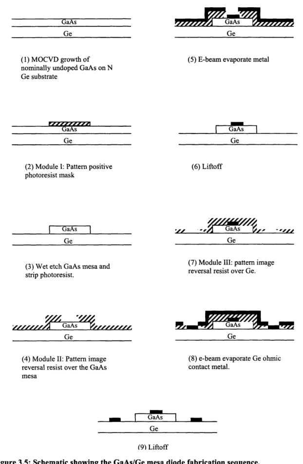
A photomask originally designed for fabricating oxide stripe laser diodes was used to fabricate the GaAs mesas diodes [6]. Though the mask was meant to fabricate stripe lasers, square geometries were obtained by first exposing the substrate vertically in the contact aligner and then rotating it by ninety degrees for the second exposure.
Figure 3.5 shows schematically the individual steps of the mesa diode fabrication process. The process consists of three modules, each module corresponding to one photo-mask level. Process Module I is the GaAs mesa formation. 200 [tmx200 ptm square GaAs mesas were etched with a phosphoric acid: hydrogen peroxide: DI water (3:1:50) solution using positive photoresist as a mask. This etchant is selective to GaAs and stops automatically when Ge is reached. Etch completion is easily observed because of the color difference between Ge (light green) and GaAs (dark blue).
20
GaAs
(1) MOCVD growth of nominally undoped GaAs on N Ge substrate
GaAs Ge
(2) Module I: Pattern positive photoresist mask
GaAs Ge
(3) Wet etch GaAs mesa and strip photoresist.
Ga,,,,s
5•%,G S ,,"
(4) Module II: Pattern image reversal resist over the GaAs mesa
(5) E-beam evaporate metal
Ge
(6) Liftoff
Ge
(7) Module III: pattern image reversal resist over Ge.
Ge
(8) e-beam evaporate Ge ohmic contact metal.
(9) Liftoff
Figure 3.5: Schematic showing the GaAs/Ge mesa diode fabrication sequence.
Process Module II is the GaAs ohmic contact formation using 'liftoff. Liftoff is a convenient micro-fabrication process that is used to pattern metallic films on a wafer. Metal is blanket-evaporated on the wafer and the metal deposited on top of the patterned photoresist is lifted away with the photoresist when soaked in acetone. Effective liftoff requires a break between the metal deposited on the photoresist and the metal deposited on the wafer. Image reversal photoresist with a negative slope profile accomplishes this. Also, as a rule of thumb the thickness of the deposited metal must be one-third the photoresist thickness for liftoff to be successful. n-GaAs ohmic contacts were formed by e-beam evaporating 500
A
Ni/ 2000 A AuGe. Alloyed ohmic contacts can be formed by heating to temperatures above the AuGe eutectic temperature of 356 oC. During alloying the Ge from the AuGe dopes the surface of the GaAs n÷ which promotes carrier tunneling and makes the contact ohmic.Process Module III is the n-Ge ohmic contact formation. This is identical to Module II except that 300 A Au/100 A Ni/2000 A AuGe/500 A Ni was e-beam evaporated to form the n-Ge contact. After liftoff of the deposited metal, the wafers were subjected to a rapid thermal anneal at 425 TC for 20s to make alloyed ohmic contacts.
3.2.4 Electrical characterization
-
Results and Discussion
A photomicrograph of the n-GaAs/n-Ge mesa diode is shown in Figure 3.6. The diode was directly micro-probed and the semilog I-V characteristic measured with a HP 4156C parameter analyzer is shown in Figure 3.7. The curve shows rectifying behavior and the series resistance estimated as the inverse slope of the I-V curve, drawn on a linear scale, at high forward bias is 10.7 Q.
It is seen from Figure 3.7 that the magnitude of the current in reverse bias is high. Thus our GaAs/Ge junction is "leaky". C-V measurements for leaky junctions to extract diode built-in voltage are not meaningful and hence were not conducted.
Figure 3.6: Photomicrograph of the fabricated GaAs/Ge mesa diode. The mesa size is 200ptmx200pm and the contact pad size is 75pmx75pm.
10-5
10-7
-2 -1 0 1 2
Bias (V)
Figure 3.7: Semi- log I-V characteristic of the GaAs/Ge diode of Figure 3.6. The Ge contact was grounded and bias on the GaAs contact was swept from negative to positive.
The theoretical I-V characteristic of the n-GaAs/n-Ge isotype junction can be predicted from the band lineups when these materials are in metallurgical contact. Figure 3.8 shows a band lineup using Anderson's rule for this material system [10, 11]. The band lineup shown is for typical doping levels. The electron work function depends on the doping level and thus the extent of band-bending will vary with doping.
For an n-n isotype junction, the majority carriers on both sides of the junction are electrons. Therefore most of the current is carried by electrons. The discontinuity in the conduction band is very small therefore, if Ge is biased negative with respect to GaAs, the electron energy in Ge increases and the electrons can easily flow in the conduction band from Ge into GaAs. On biasing GaAs negative with respective to Ge, electrons from GaAs flow into Ge. Thus the electron flow is not impeded much in either state of bias. Hence in the ideal theoretical case the n-GaAs/n-Ge diodes should not rectify. This has also been experimentally found by Hudait et al. [7].
Ge Bandgap = 0.661eV GaAs Bandgap = 1.42eV
Ge Electron Affinity =4.0eV GaAs Electron Affinity =4.07eV
Vacuum Vacuum
E ,
u
E - - -- - --- --- - ---- - - E FVc---
---
---
EFE, - E,
n-Ge n*-GaAs n-Ge n -GaAs
Band Profile of disconnected n-Ge and n+-GaAs Discontinuity in Conduction Band =
AElectron Affinity = (4.07-4.0)=0.07eV
Discontinuity in Valence Band = AEg+
AElectron Affinity = 0.759+0.07=0.83eV
Figure 3.8: Band lineup for the n-Gel n+-GaAs heterojunction.
The rectifying I-V curve of Figure 3.7 suggests that a thin layer of p+-Ge is sandwiched between n-GaAs and n-Ge due to autodoping by Ga atoms. Thus the structure is actually n+-GaAs/p÷-Ge/n-Ge rather than simply n+-GaAs/n-Ge. A similar
observation has been made by Wojtczuk et al. [9].The rectifying I-V can be explained by modeling the n-p-n structure as two diodes of opposing polarities in series as shown in Figure 3.9. The I-V plot of Figure 3.7 was obtained by grounding terminal 2 (Figure 3.9) and sweeping the bias on terminal 1 from negative to positive. When a negative bias is applied to terminal 1, the n+-GaAs/p'-Ge diode is forward-biased and the p+-Ge/n+-Ge homodiode is reverse biased. Since these diodes are in series, the net current is limited by the reverse biased homodiode and hence is small. When a positive voltage is applied to n'-GaAs, the n*-GaAs/p+-Ge diode is reverse biased and the p+-Ge/n'-Ge homodiode is forward biased. It is believed that the observed high current in this configuration is because the reverse-biased n'-GaAs/p'-Ge junction behaves as a tunnel diode since both the GaAs and Ge are autodoped in excess of their effective density of states. A tunnel diode in reverse bias does not impede current as much as a reversed biased conventional diode. Hence with the n+-GaAs biased positive, the n-p-n structure effectively behaves as a forward biased Ge p-n homodiode and passes high current. At sufficiently high forward bias, the diode resistance can be assumed to be zero, and the resistance between the terminals equals the bulk resistance (RGaAs+RGe).
RGaAs n+-GaAs/p+-Ge RGe
1 2
p'-Ge/n-Ge
Figure 3.9: The n-p-n diode structure and the equivalent electrical circuit.
In summary, it can be concluded that Ga does indeed diffuse into Ge during the MOCVD growth of GaAs on Ge and acts as an electrically active p-type dopant. The voltage drop across the n-GaAs/n-Ge junction is attributed to the forward biased p+-Ge/n-Ge homodiode. Since the homodiode will be positively biased during the LED operation,
the forward resistance is small and a bias current can be passed through the LED without incurring a huge voltage drop across the GaAs/Ge junction.
3.3 The p++-Si /p+-GaAs heterojunction
In order to study the electrical characteristics of the p++-Si/p+-GaAs heterojunction, a 0.5 rm p+'-Si (boron doped)/ 2pm p+-GaAs (zinc doped) stack was grown by MOCVD on a semi-insulating GaAs substrate. The heavy doping should cause carrier tunneling and make the Si/GaAs heterojunction nearly ohmic with a low resistance.
3.3.1 Material characterization -SIMS Analysis
The SIMS profile of B, Ga and As species in the p"+-Si/p÷-GaAs stack is shown in Figure 3.10. Note that zero on the x-axis corresponds to the Si surface and the Si/GaAs interface is approximately 0.45 gm from the surface. In the Si layer, the boron concentration is very high and the gallium concentration is higher than arsenic away from the Si/GaAs interface. It is seen that though Si is autodoped by Ga and As, the high intentional boron doping swamps the Ga and As concentrations and so the p++-Si preserves its doping level and type.
1E22 -o 1E21 E 0 a 1E20 o 1E19 0 1E18 1E17 0.0 0.2 0.3 0.4 0.5 0.6 Depth (ýpm)
Figure 3.10: SIMS profile of Ga, As and B species in the p++-Si/p+-GaAs stack.
3.3.2 Electrical characterization
-
Mesa diode Fabrication
The mesa diode structure (see Figure 3.11) and basic fabrication sequence are similar to the GaAs/Ge diode process with a few modifications to accommodate the new material system. The mesa formation step first required the dry etching of 0.5 ptm p+ Si in an ECR enhanced RIE system using a SF6/02 plasma for 200s. The removal of the Si layer is easily visible as there is a color difference between Si (native silicon dioxide formed on Si is yellow green) and GaAs (dark blue). The dry etch recipe can be found in Appendix C. After the Si dry etch, 0.4 ýpm of p'-GaAs was wet chemical etched for 4 minutes (etch rate - 0.1 p.m/min) using H3PO4: H202: H20 (3:1:50). Thus a 0.9 ptm
Si/GaAs mesa was formed. After patterning the top contact area, a quick dilute HF dip (1:10 HF:DI) was used to remove the Si native oxide and the wafer was immediately loaded in the e-beam chamber for metal deposition. A 500 A Ti/1000 A Al stack was used to contact the p+-Si. After patterning the bottom contact area, a 50 A Ti/200 A
Pt/2500 A Au stack was e-beam evaporated to form the p+-GaAs ohmic contact. Subsequent to the metal deposition and liftoff processes, the wafer was furnace annealed
at 400 OC for 40 minutes in a forming gas (90% N2:10% H2) ambient to form good ohmic contacts.
500A Ti/ 1000 A A
05 A Ti/ 200A Pt /2500A Au
-1.6pm
Figure 3.11: Schematic of the p++-Si/ p÷-GaAs mesa diode.
3.3.3 Electrical characterization
-
Results and Discussion
The fabricated diodes were directly micro-probed and I-V characteristic measured with a HP 4156C parameter analyzer. Figure 3.12 shows the I-V characteristic. The characteristic is near linear (ohmic) over a wide range of applied voltages. It is believed that this is due to the tunneling of carriers across the heavily doped Si/GaAs junction.
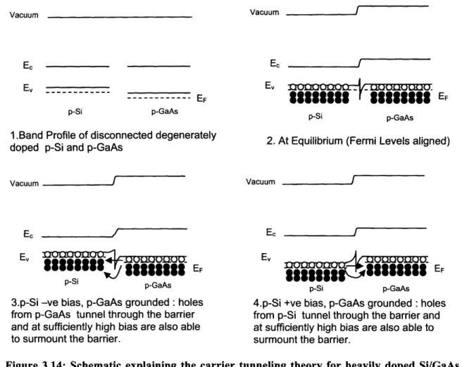
In a p-GaAs/p-Si isotype junction the majority carriers on both sides of the junction are holes. Therefore the discontinuity in the valence band dictates the current flow (see Figure 3.13). Since the electron affinity of Si and GaAs are nearly the same, the discontinuity in the valence band is relatively large and approximately equal to the difference in bandgap energy of the materials (0.32 eV). Hence in theory the p-Si/p-GaAs junction should be non-ohmic. Since we have doped the Si and GaAs very heavily, we expect the holes to tunnel through the valence band discontinuity (Figure 3.14) and therefore the observed turn on voltage is very small.
The band diagrams in Figure 3.13 and 3.14 are for an ideal junction with no interface states. In reality, the 4% lattice mismatch for the Si/GaAs system leads to a high density of dangling bonds and correspondingly a high density of interface states. These interface states are a major factor in determining the energy band diagram of the
0.10 C 0.05 -1 -0.05 -0.10 0.5 1.0 5
/)
Figure 3.12: I-V characteristic for the p++-Si/ p÷-GaAs diode.
Si Bandgap = 1.12eV Si Electron Affinity =4.05eV
Vacuum
GaAs Bandgap = 1.42eV
GaAs Electron Affinity =4.07eV
Vacuum /'
- EF
J --- EF
p-Si p-GaAs p-Si p-GaAs
Band Profile of disconnected P-Si and P- GaAs Discontinuity in Conduction Band = AElectron Affinity =(4.07-4.05)=0.02eV
Discontinuity in Valence Band = AE,+
AElectron Affinity = 0.3+0.02=0.32eV Figure 3.13: Band lineup for p-Si /p-GaAs material system.
Va~ri Vauu
p-Si
--- EF
p-GaAs
1.Band Profile of disconnected degenerately doped p-Si and p-GaAs
Vacuum
Ec /
1Ev EF
p-Si p-GaAs
3.p-Si -ve bias, p-GaAs grounded : holes from p-GaAs tunnel through the barrier and at sufficiently high bias are also able to surmount the barrier.
Ec /
383333
r
LUUUUg
EFp-Si p-GaAs
2. At Equilibrium (Fermi Levels aligned)
Vacuum
=M888
EFp-Si p-GaAs
4.p-Si +ve bias, p-GaAs grounded : holes from p-Si tunnel through the barrier and at sufficiently high bias are also able to surmount the barrier.
Figure 3.14: Schematic explaining the carrier tunneling theory for heavily doped Si/GaAs junction.
3.4 The p++-Ge/p+-GaAs heterojunction
One alternative to encapsulating the LED with Si is to use Ge which is also considered CMOS compatible. To investigate the p++-Ge/p+-GaAs heterojunction, 0.5 gm boron doped Ge/1 pm Zn doped GaAs was grown by MOCVD and processed into diodes. The fabrication of the p++-Ge/p÷-GaAs mesa diode is identical to the previous diodes except for a few changes to accommodate the new material system. The mesa was formed by dry etching the Ge using an SF6/02 plasma. The p÷t -Ge was contacted using 500 A Ti/ 250
A
Al. The SIMS data and I-V characteristic for this heterojunction are shown in Figures 3.15 and 3.16. The linear I-Vs indicate an ohmic junction.Vacuum
Ecuum
P"+Ge/P+GaAs
0.5 1.0 1.5 2.0 2.5
Depth (microns)
Figure 3.15: SIMS profile of the B, Zn concentrations in the p++-Ge/p÷-GaAs stack.
1E21 1E20 1E19 1E18 1E17 1E16 1E15
0.10
0.05
-1.0
-0.10
ts)
Figure 3.16: I-V characteristic of the p++-Ge/p+-GaAs heterojunction.
3.5 CMOS-compatible ohmic contacts to Ge
Referring back to the CMOS-compatible LED design in Figure 3.1, the n-GaAs cathode of the LED is contacted through the underlying n-Ge film to avoid etching the III-V material. Since the usual ohmic contacts to n-Ge are non CMOS compatible other alternatives have to be studied.
Two metal systems namely Ni and Ti were investigated. Ge wafer with n-type doping densities on the order of 5x10'8 cm-3 were used for this study. Due to the limited
availability of Ge substrates in our facilities, the Ge substrates used for this study were recycled by selectively etching the epitaxial n-GaAs and revealing the underlying heavily As autodoped (Figure 3.3) n-Ge substrates. Liftoff and e-beam evaporation were used to deposit 100 ptmx100 [tm square metal contacts on the wafer.
Figure 3.17 shows the I-V curves for NiGe-contacted Ge obtained for different annealing temperatures. It is seen that low resistance (15 Q) NiGe ohmic contacts are
formed for 350 oC, 40 min anneal conditions. Figure 3.18 is the I-V characteristic for TiGe-contacted Ge. The series resistance is 18.9 n. Though TiGe contacts show a higher resistance than NiGe contacts, TiGe was ultimately used in this work as the CMOS-compatible contact metallurgy due to nonavailability of a Ni source in the sputtering system. r" 4v"% 0.08 0.06 0.04 0.02 -1 -0.06 -0.08 3500C 4500C 0.5 1.0 1.5 Voltage (V)
Figure 3.17: I-V characteristic for NiGe contact for different annealing conditions.
I*~ r~o
S0.06
0.02
-1 5
Figure 3.18: I-V characteristic of TiGe contacted Ge. Ti/Al was annealed in forming gas ambient at 400 'C for 40min to form TiGe.
In summary, a better understanding of the n-GaAs/n-Ge and p"+-Si/p -GaAs heterojunctions was gained in this chapter. The current-voltage characteristic of the n-GaAs/n-Ge junction showed rectification indicating presence of a p Ge layer and suggests that the n-GaAs/p÷-Ge interface is a tunnel junction. Thus, the forward voltage drop across the n-GaAs/n-Ge junction can be attributed to the forward biased p÷-Ge/n-Ge homodiode. The current-voltage characteristic of the p÷÷-Si/p÷-GaAs heterojunctions are nearly linear showing that carrier tunneling helps reduce resistance.