Design Decisions in the Implementation of a
Raw Architecture Workstation
by
Michael Bedford Taylor
A.B., Dartmouth College 1996
Submitted to the Department of Electrical Engineering and Computer Science
in partial fulfillment of the requirements for the degree of
Master of Science
at the
MASSACHUSETTS INSTITUTE OF TECHNOLOGY
September 1999
© MCMXCIX Massachusetts Institute of Technology.
All rights reserved.
S ignature of A uthor ...
Department of Electrical Engineering and Computer Science
September 9, 1999
C ertified b y ...
Anant Agarwal
Associate Professor of Electrical Engineering and Computer Science
Thesis Supervisor
A ccep ted b y ...
Arthur C. Smith
Chairman, Departmental Committee on Graduate Students
Design Decisions in the Implementation of a
Raw Architecture Workstation
by
Michael Bedford Taylor
Submitted to the
Department of Electrical Engineering and Computer Science
MASSACHUSETTS INSTITUTE OF TECHNOLOGY
September 9, 1999
in partial fulfillment of the requirements for the degree of
Master of Science in Electrical Engineering and Computer Science.
Abstract
In this thesis, I trace the design decisions that we have made along the journey to
creating the first Raw architecture prototype. I describe the emergence of extroverted
computing, and the consequences of the billion transistor era. I detail how the
architec-ture was born from our experience with FPGA computing. I familiarize the reader with
Raw by summarizing the programmer's viewpoint of the current design. I motivate
our decision to build a prototype. I explain the design decisions we made in the
imple-mentation of the static and dynamic networks, the tile processor, the switch processor,
and the prototype systems. I finalize by showing some results that were generated by
our compiler and run on our simulator.
Thesis Supervisor: Anant Agarwal
Dedication
This thesis is dedicated to my mom.
TABLE OF CONTENTS
1 INTRODUCTION
5
2 EARLY DESIGN DECISIONS
9
3 WHAT WE'RE BUILDING
11
4 STATIC NETWORK DESIGN
19
5
DYNAMIC NETWORK
26
6 TILE PROCESSOR DESIGN
28
7 1/0 AND MEMORY SYSTEM
34
8DEADLOCK
37
9 MULTITASKING
46
10 THE MULTICHIP PROTOTYPE
48
11 CONCLUSIONS
50
1
INTRODUCTION
1.0 MANIFEST
In the introduction of this thesis, I start by motivat-ing the Raw architecture discipline, from a computer architect's viewpoint.
I then discuss the goals of the Raw prototype pro-cessor, a research implementation of the Raw philoso-phy. I elaborate on the research questions that the Raw group is trying to answer.
In the body of the thesis, I will discuss some of the important design decisions in the development of the Raw prototype, and their effects on the overall
develop-ment.
Finally, I will conclude with some experimental numbers which show the performance of the Raw proto-type on a variety of compiled and hand-coded programs. Since the prototype is not available at the time of this thesis, the numbers will come from a simulation which matches the synthesizeable RTL verilog model on a cycle by cycle basis.
1.1 MOTIVATION FOR A NEW TYPE OF PROCESSOR 1.1.1 The sign of the times
The first microprocessor builders designed in a period of famine. Silicon area on die was so small in the early seventies that the great challenge was just in achieving important features like reasonable data and address widths, virtual memory, and support for external I/O.
A decade later, advances in material science pro-vided designers with enough resources that silicon was neither precious nor disposable. It was a period of mod-eration. Architects looked to advanced, more space con-suming techniques like pipelining, out-of-order issue, and caching to provide performance competitive with minicomputers. Most of these techniques were bor-rowed from supercomputers, and were carefully added from generation to generation as more resources became available.
The next decade brings with it a regime of excess. We will have billions of transistors at our disposal. The new challenge of modern microprocessor architects is very simple: we need to provide the user with an effec-tive interface to the underlying raw computational resources.
1.1.2 An old problem: Specint
In this new era, we could continue on as if we still lived in the moderation phase of microprocessor devel-opment. We would incrementally add micro-architec-tural mechanisms to our superscalar and VLIW processors, one by one, carefully measuring the bene-fits.
For today's programs, epitomized by the SpecInt95 benchmark suite, this is almost certain to provide us with the best performance. Unfortunately, this approach suffers from exponentially growing complexity (mea-sured by development and testing costs and man-years) that is not being sufficiently mitigated by our sophisti-cated design tools, or by the incredible expertise that we have developed in building these sorts of processors. Unfortunately, this area of research is at a point where increasing effort and increasing area is yielding dimin-ishing returns [Hennessey99].
Instead, we can attack a more fuzzy, less defined goal. We can use the extra resources to expand the scope of problems that microprocessors are skilled at solving. In effect, we redirect our attention from making proces-sors better at solving problems they are already, frankly, quite good at, towards making them better at application domains which they currently are not so good at.
In the meantime, we can continue to rely on the as-yet juggernaut march of the fabrication industry to give us a steady clock speed improvement that will allow our existing SpecInt applications to run faster than ever.
1.1.3 A new problem: Extroverted computing Computers started out as very oblivious, introverted devices. They sat in air-conditioned rooms, isolated from their users and the environment. Although they communicated with EACH OTHER at high speeds, the bandwidth of their interactions with the real world was amazingly low. The primary input devices, keyboards, provided at most tens of characters per second. The out-put bandwidth was similarly pathetic.
With the advent of video display and sound synthe-sis, the output bandwidth to the real world has blos-somed to 10s of megabytes per second. Soon, with the advent of audio and video processing, the input band-width will match similar levels.
As a result of this, computers are going to become more and more aware of their environments. Given suf-ficient processing and 1/0 resources, they will not only become passive recorders and childlike observers of the environment, they will be active participants. In short, computers will turn from recluse introverts to extro-verts.
The dawn of the extroverted computing age is upon us. Microprocessors are just getting to the point where they can handle real-time data streams coming in from and out to the real world. Software radios and cell phones can be programmed in a 1000 lines of C++ [Tennenhouse95]. Video games generate real-time video, currently with the help of hardware graphics back ends. Real-time video and speech understanding, searching, generation, encryption, and compression are on the horizon. What once was done with computers for text and integers will soon be done for analog signals. We will want to compose sound and video, search it, interpret it, and translate it.
Imagine, while in Moscow, you could talk to your wrist watch and tell it to listen to all radio stations for the latest news. It would simultaneously tune into the entire radio spectrum (whatever it happens to be in Rus-sia), translate the speech into English, and index and compress any news on the U.S. At the same time, your contact lens display would overlay English translations of any Russian word visible in your sight, compressing and saving it so that you can later edit a video sequence for your kids to see (maybe you'll encrypt the cab ride through the red light district with DES-2048). All of these operations will require massive bandwidth and processing.
1.1.4 New problem, old processors?
We could run our new class of extroverted applica-tions on our conventional processors. Unfortunately,
these processors are, well, introverted.
First off, conventional processors often treat 1/0 processing as a second class citizen to memory process-ing. The 1/0 requests travel through a hierarchy of slower and slower memory paths, and end up being bot-tlenecked at the least common denominator. Most of the
pins are dedicated to caches, which ironically, are intended to minimize communication with the outside world. These caches, which perform so well on conven-tional computations, perform poorly on streaming, extroverted, applications which have infinite data
streams that are briefly processed and discarded. Secondly, these new extroverted applications often have very plentiful fine grained parallelism. The con-ventional ILP architectures have complicated, non-scal-able structures (multi-ported or rotating register files, speculation buffers, deferred exception mechanisms, pools of ALUs) that are designed to wrest small degrees of parallelism out of the most twisty code. The parallel-ism in these new applications does not require such sophistication. It can be exploited on architectures that are easy to design and are scalable to thousands of active functional units.
Finally, the energy efficiency of architectures needs to be considered to evaluate their suitability for these new application domains. The less power microproces-sors need, the more and more environments they can exist in. Power requirements create a qualitative differ-ence along the spectrum of processors. Think of the enormous difference among 1) machines that require large air conditioners, 2) ones that need to be plugged in, 3) ones that run on batteries, and ultimately, 4) ones that runs off their tiny green chlorophyllic plastic case. 1.1.5 New problems, new processors.
It is not unlikely that existing processors can be modified to have improved performance on these new applications. In fact, the industry has already made some small baby steps with the advent of the Altivec and MAX-2 technologies [Lee96].
The Raw project is creating an extroverted architec-ture from scratch. We take as our target these data-inten-sive extroverted applications. Our architecture is extremely simple. Its goal is to expose as much of the copious silicon and pin resources to these applications. The Raw architecture provides a raw, scalable, parallel interface which allows the application to make direct use of every square millimeter of silicon and every 1/0 pin. The 1/0 mechanism allows data to be streamed directly in and out of the chip at extraordinary rates.
The Raw architecture discipline also has advan-tages for energy efficiency. However, they will not be discussed in this thesis.
1.2 MY THESIS AND HOW IT RELATES TO RAW My thesis details the decisions and ideas that have shaped the development of a prototype of the new type of processor that our group has developed. This process has been the result of the efforts of many talented peo-ple. When I started at MIT three years ago, the Raw project was just beginning. As a result, I have the luxury of having a perspective on the progression of ideas through the group. Initially, I participated in much of the data gathering that refined our initial ideas. As time passed on, I became more and more involved in the development of the architecture. I managed the two sim-ulators, hand-coded a number of applications, worked on some compiler parallelization algorithms, and even-tually joined the hardware project. I cannot claim to have originated all of the ideas in this thesis; however I can reasonably say that my interpretation of the sequence of events and decisions which lead us to this design point probably is uniquely mine. Also uniquely mine probably is my particular view of what Raw should look like.
Anant Agarwal and Saman Amarasinghe are my fearless leaders. Not enough credit goes out to Jonathan Babb, and Matthew Frank, whose brainstorming planted the first seeds of the Raw project, and who have contin-ued to be a valuable resource. Jason Kim is my partner in crime in heading up the Raw hardware effort. Jason Miller researched 1/0 interfacing issues, and is design-ing the Raw handheld board. Mark Stephenson, Andras Moritz, and Ben Greenwald are developing the hard-ware/software memory system. Ben, our operating sys-tems and tools guru also ported the GNU binutils to Raw. Albert Ma, Mark Stephenson, and Michael Zhang crafted the floating point unit. Sam Larsen wrote the static switch verilog. Rajeev Barua and Walter Lee cre-ated our sophisticcre-ated compiler technology. Elliot Wain-gold wrote the original simulator. John Redford and Chris Kappler lent their extensive industry experience to the hardware effort.
1.2.1 Thesis statement
The Raw Prototype Design is an effective design for a research implementation of a Raw architecture workstation.
1.2.2 The goals of the prototype
In the implementation of a research prototype, it is important early on to be excruciatingly clear about one's goals. Over the course of the design, many implementa-tion decisions will be made which will call into quesimplementa-tion these goals. Unfortunately, the "right" solution from a purely technical standpoint may not be the correct one for the research project. For example, the Raw prototype has a 32-bit architecture. In the commercial world, such a paltry address space is a guaranteed trainwreck in the era of gigabit DRAMs. However, in a research proto-type, having a smaller word size gives us nearly twice as much area to further our research goals. The tough part is making sure that the implementation decisions do not
invalidate the research's relevance to the real world. Ultimately, the prototype must serve to facilitate the exploration and validation of the underlying research hypotheses.
The Raw project, underneath it all, is trying to answer two key research questions:
1.2.3 The Billion Transistor Question
What should the billion transistor processor of the year 2007 look like?
The Raw design philosophy argues for an array of replicated tiles, connected by a low latency, high throughput, pipelined network.
This design has three key implementation benefits, relative to existing superscalar and VLIW processors:
First, the wires are short. Wire length has become a growing concern in the VLSI community, now that it takes several cycles for a signal to cross the chip. This is not only because the transistors are shrinking, and die sizes are getting bigger, but because the wires are not scaling with the successive die shrinks, due to capacitive and resistive effects. The luxurious abstraction that the delay through a combinational circuit is merely the sum of its functional components no longer holds. As a result, the chip designer must now worry about both congestion AND timing when placing and routing a cir-cuit. Raw's short wires make for an easy design.
Second, Raw is physically scalable. This means that all of the underlying hardware structures are scalable. All components in the chip are of constant size, and do not grow as the architecture is adapted to utilize larger and larger transistor budgets. Future generations of a Raw architecture merely use more tiles with out nega-tively impacting the cycle time. Although Raw offers
scalable computing resources, this does not mean that we will necessarily have scalable performance. That is dependent on the particular application.
Finally, Raw has low design and verification com-plexity. Processor teams have become exponentially larger over time. Raw offers constant complexity, which does not grow with transistor budget. Unlike today's superscalars and VLIWs, Raw does not require a rede-sign in order to accommodate configurations with more or fewer processing resources. A Raw designer need only design the smaller region of a single tile, and repli-cate it across the entire die. The benefit is that the designer can concentrate all of one's resources on tweaking and testing a single tile, resulting in clock speeds higher than that of monolithic processors. 1.2.4 The "all-software hardware" question What are the trade-offs of replacing conventional hardware structures with compilation and software technology?
Motivated by advances in circuit compilation tech-nology, the Raw group has been actively exploring the idea of replacing hardware sophistication with compiler smarts. However, it is not enough merely to reproduce the functionality of the hardware. If that were the case, we would just prove that our computing fabric was Tur-ing-general, and move on to the next research project. Instead our goal is more complex. For each alternative solution that we examine, we need to compare its area-efficiency, performance, and complexity to that of the equivalent hardware structure. Worse yet, these numbers need to be tempered by the application set which we are targeting.
In some cases, like in leveraging parallelism, removing the hardware structures allows us to better manage the underlying resources, and results in a per-formance win. In other cases, as with a floating point unit, the underlying hardware accelerates a basic func-tion which would take many cycles in software. If the target application domain makes heavy use of floating point, it may not be possible to attain similar perfor-mance per unit area regardless of the degree of compiler smarts. On the other hand, if the application domain does not use floating point frequently, then the software approach allows the application to apply that silicon area to some other purpose.
1.3 SUMMARY
In this section, I have motivated the design of a new family of architectures, the Raw architectures. These architectures will provide an effective interface for the amazing transistor and pin budgets that will come in the next decade. The Raw architectures anticipate the arrival of a new era of extroverted computers. These extroverted computers will spend most of their time interacting with the local environment, and thus are optimized for processing and generating infinite, real-time data streams.
I continued by stating my thesis statement, that the Raw prototype design is an effective design for a research implementation of a Raw architecture worksta-tion. I finished by explaining the central research ques-tions of the Raw project.
2
EARLY DESIGN
DECISIONS
2.0 THE BIRTH OF THE FIRST RAW ARCHITECTURE 2.0.1 RawLogic, the first Raw prototype
Raw evolved from FPGA architectures. When I arrived at MIT almost three years ago, Raw was very much in its infancy. Our original idea of the architecture was as a large box of reconfigurable gates, modeled after our million-gate reconfigurable emulation system. Our first major paper, the Raw benchmark suite, showed very positive results on the promise of configurable logic and hardware synthesis compilation. We achieved speedups on a number of benchmarks; numbers that were crazy and exciting [Babb97].
However, the results of the paper actually consider-ably matured our viewpoint. The term "reconfigurable logic" is really very misleading. It gives one the impres-sion that silicon atoms are actually moving around inside the chip to create your logic structures. But the reality is, an FPGA is an interpreter in much the same way that a processor is. It has underlying programmable hardware, and it runs a software program that is inter-preted by the hardware. However, it executes a very small number of very wide instructions. It might even be viewed as an architecture with a instruction set opti-mized for a particular application; the emulation of digi-tal circuits. Realizing this, it is not surprising that our experiences with programming FPGA devices show that they are neither superior nor inferior to a processor. It is merely a question of which programs run better on which interpreter.
In retrospect, this conclusion is not all that surpris-ing; we already know that FPGAs are better at logic emulation than processors; otherwise they would not exist. Conversely, it is not likely that the extra bit-level flexibility of the FPGA comes for free. And, in fact, it does not. 32-bit datapath operations like additions and multiplies perform much more quickly when optimized by an Intel circuit hacker on a full-custom VLSI process than when they are implemented on a FPGA substrate. And again, it is not much wonder, for the processor's multiplier has been realized directly in silicon, while the multiplier implementation on the FPGA is running under one level of interpretation.
2.0.2 Our Conclusions, based on Raw logic In the end, we identified three major strengths of FPGA logic, relative to a microprocessor:
FPGAs make a simple, physically scalable parallel fabric. For applications which have a lot of parallelism, we can easily exploit it by adding more and more fabric. FPGAs allow for extremely fast communication and synchronization between parallel entities.
In the realm of shared memory multiprocessors, it takes tens to hundreds of cycles for parallel entities to communication and synchronize [Agarwal95]. When a silicon compiler compiles parallel verilog source to an FPGA substrate, the different modules can communi-cate on a cycle-by-cycle basis. The catch is that this communication often must be statically scheduled. FPGAs are very effective at bit and byte-wide data manipulation.
Since FPGA logic functions operate on small bit quantities, and are designed for circuit emulation, they are very powerful bit-level processors.
We also identified three major strengths of proces-sors relative to FPGAs:
Processors are highly optimized for datapath ori-ented computations.
Processors have been heavily pipelined and have custom circuits for datapath operations. This customiza-tion means that they process word-sized data much faster than an FPGAs.
Compilation times are measure in seconds, not hours [Babb97].
The current hardware compilation tools are very computationally intensive. In part, this is because the hardware compilation field has very different require-ments from the software compilation field. A smaller, faster circuit is usually much more important than fast compilation. Additionally, the problem sizes of the FPGA compilers are much bigger -- a net list of NAND gates is much larger than a dataflow graph of a typical program. This is exacerbated by the fact that the synthe-sis tools decompose identical macro-operations like 32-bits adds into separately optimized netlists of bit-wise operations.
through two types of high performance, pipelined
net-Processors are very effective for just getting through works: one static and one dynamic.
the millions of lines of code that AREN'T the inner
loop. Now, two years later, we are on the cusp of building the first prototype of this new architecture.
The so-called 90-10 rule says that 90 percent of the time is spent in 10 percent of the program code. Proces-sor caches are very effective at shuffling infrequently used data and code in and out of the processor when it is not needed. As a result, the non-critical program por-tions can be stored out to a cheaper portion of the mem-ory hierarchy, and can be pulled in at a very rapid rate when needed. FPGAs, on the other hand, have a very small number (one to four) of extremely large, descrip-tive instructions stored in their instruction memories. These instructions describe operations on the bit level, so a 32-bit add on an FPGA takes many more instruc-tion bits than the equivalent 32-bit processor instrucinstruc-tion. It often takes an FPGA thousands or millions of cycles to load a new instruction in. A processor, on the other hand, can store a large number of narrow instruction in its instruction memory, and can load in new instructions in a small number of cycles. Ironically, the fastest way for an FPGA to execute reams of non-loop-intensive code is to build a processor in the FPGA substrate. However, with the extra layer of interpretation, the FPGA's performance will not be comparable to a pro-cessor built in the same VLSI process.
2.0.3 Our New Concept of a Raw Processor
Based on our conclusions, we arrived at a new model of the architecture, which is described in the Sep-tember 1997 IEEE Computer "Billion Transistor" issue [Waingold97].
We started with the FPGA design, and added coarse grained functional units, to support datapath operations. We added word-wide data memories to keep frequently used data nearby. We left in some FPGA-like logic to support fine grained applications. We added pipelined sequencers around the functional units to support the reams of non-performance critical code, and to simplify compilation. We linked the sequenced functional units with a statically scheduled pipelined interconnect, to mimic the fast, custom interconnect of ASICs and FPGAs. Finally, we added a dynamic network to support dynamic events.
The end result: a mesh of replicated tiles, each con-taining a static switch, a dynamic switch, and a small pipelined processor. The tiles are all connected together
3
WHAT WE'RE
BUILDING
3.0 THE FIRST RAW ARCHITECTURE
In this section, I present a description of the archi-tecture of the Raw prototype, as it currently stands, from an assembly language viewpoint. This will give the reader a more definite feel for exactly how all of the pieces fit together. In the subsequent chapters, I will dis-cuss the progress of design decisions which made the architecture the way it is.
3.0.1 A mesh of identical tiles
A Raw processor is a chip containing a 2-D mesh of identical tiles. The tiles are connected to its nearest neighbors by the dynamic and static networks. To pro-gram the Raw processor, one propro-grams each of the indi-vidual tiles. See the figure entitled "A Mesh of Identical Tiles."
3.0.2 The tile
Each tile has a tile processor, a static switch proces-sor, and a dynamic router. In the rest of this document, the tile processor is usually referred to as "the main
pro-cessor," "the propro-cessor," or "the tile processor." "The Raw processor"- refers to the entire chip -- the networks and the tiles.
The tile processor uses a 32-bit MIPS instruction set, with some slight modifications. The instruction set is described in more detail in the "Raw User's Manual," which has been appended to the end of this thesis.
The switch processor (often referred to as "the switch") uses a MIPS-like instruction set that has been stripped down to contain just moves, branches, jumps and branches. Each instruction also has a ROUTE com-ponent, which specifies the transfer of values on the static network between that switch and its neighboring switches.
The dynamic router runs independently, and is under user control only indirectly.
3.0.3 The tile processor
The tile processor has a 32 Kilobyte data memory, and a 32 Kilobyte instruction memory. Neither of them are cached. It is the compiler's responsibility to virtual-ize the memories in software, if this is necessary.
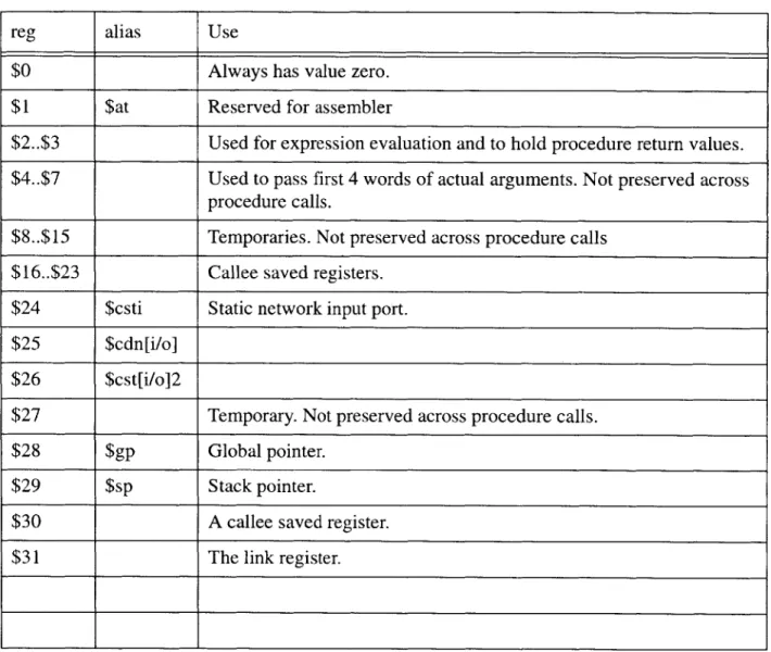
The tile processor communicates with the switch through two ports which have special register names, $csto and $csti. When a data value is written to $csto, it is actually sent to a small FIFO located in the switch.
network wires
When a data value is read from $csti, it is actually read from a FIFO inside the switch. The value is removed from the FIFO when the read occurs.
If a read on $csti is specified, and there is no data available from that port, the processor will block. If a write to $csto occurs, and the buffer space has been filled, the processor will also block.
Here is some sample assembly language: # XOR register 2 with 15,
# and put result in register 31
xori $31,$2,15
# get value from switch, add to # register 3, and put result # in register 9
addu $9,$3,$csti
# an ! indicates that the result # of the operation should also
# be written to $csto
and! $0,$3,$2
# load from address at $csti+25
# put value in register 9 AND # send it through $csto port
# to static switch
ld! $9,25($csti)
# jump through value specified
# by $csti
j $csti
nop # delay slot
The dynamic network ports operate very similarly. The input port is $cdni, and the output port is $cdno. However, instead of showing up at the static switch, the messages are routed through the chip to their destination tile. This tile is specified by the first word that is written into $cdno. Each successive word will be queued up until a dlaunch instruction is executed. At that point, the message starts streaming through the dynamic net-work to the other tile. The next word that is written into $cdno will be interpreted as the destination for a new dynamic message.
addiu $cdno,$0,15
# put in a couple of datawords, # one from register 9 and the other
# from the csti network port or $cdno,$O,$9
ld $cdno,$O,$csti
# launch the message into the # network
dlaunch
# if we were tile 15, we could
# receive our message with: # read first word
or $2,$cdni,$O
# read second word, or $3, $cdni, $0
# the header word is discarded
# by the routing hardware, so
# the recipient does not see it # there are only two words in # this message
3.0.4 The switch processor
The switch processor has a local 8096-instruction instruction memory, but no data memory. This memory is also not cached, and must be virtualized in software
by the switch's nearby tile processor.
The switch processor executes a very basic instruc-tion set, which consists of only moves, branches, jumps, and nops. It has a small, four element register file. The destinations of all of the instructions must be registers. However, the sources can be network ports. The net-work port names for the switch processor are $csto, $csti, $cNi, $cEi, $cSi, $cWi, $cNo, $cEo, $cSo and $cWo. These correspond to the main processor s output queue, the main processor's input queue, the input queues coming from the switch's four neighbors, and the output queues going out to the switch's four neigh-bors.
Each switch processor instruction also has a ROUTE component, which is executed in parallel with the instruction component. If any of the ports specified
in the instruction are full (for outputs) or empty (for inputs), the switch processor will stall.
# branch instruction
beqz $9, target nop
# branch if processor # sends us a zero
beqz $csto, target nop
# branch if the value coming
# from the west neighbor is a zero
beqz $cWi, target nop
# store away value from # east neighbor switch
move $3, $cEi
# same as above, but also route
# the value coming from the north
# port to the south port
move $3, $cEi route $cNi->$cSo
# all at the same time:
# send value from north neighbor # to both the south and processor # input ports.
# send value from processor to west
# neighbor.
# send value from west neighbor to
# east neighbor
nop route $cNi->$cSo, $cNi->$csti, $csto->$cWo, $cWi->$cEo
# jump to location specified
# by west neighbor and route that # location to our east neighbor jr $cWi
nop
route $cWi->$cEo
3.0.5 Putting it all together
For each switch-processor, processor-switch, or switch-switch link, the value arrives at the end of the
cycle. The code below shows the switch and tile code required for a tile-to-tile send.
TILE 0:
or $csto,$O,$5
SWITCH 0:
nop route $csto->$cEo SWITCH 1:
nop route $cWi->$csti TILE 1:
and $5, $5, $csti
This code sequence takes five cycles to execute. In the first cycle, tile 0 executes the OR instruction, and the value arrives at switch 0. On the second cycle, switch 0 transmits the value to switch 1. On the third cycle, switch I transfers the value to the processor. On the fourth cycle, the value enters the decode stage of the processor. On the fifth cycle, the AND instruction is executed.
Since two of those cycles were spent performing useful computation, the send-to-use latency is three cycles.
More information on programming the Raw archi-tecture can be found in the User's Manual at the end of this thesis. More information on how our compiler par-allelizes sequential applications for the Raw architecture can be found in [Lee98] and [Barua99].
3.1 RAW MATERIALS
Before we decided what we were going to build for the prototype, we needed to find out what resources we had available to us. Our first implementation decision, at the highest level, was to build the prototype as a stan-dard-cell CMOS ASIC (application specific integrated circuit) rather than as full-custom VLSI chip.
In part, I believe that this decision reflects the fact that the group's strengths and interests center more on systems architecture than on circuit and micro-architec-tural design. If our research shows that our software sys-tems can achieve speedups on our micro-architecturally unsophisticated ASIC prototype, it is a sure thing that
the micro-architects and circuit designers will be able to carry the design and speedups even further.
3.1.1 The ASIC choice
When I originally began the project, I was not entirely clear on the difference between an ASIC and full-custom VLSI process. And indeed, there is a good reason for that; the term ASIC (application specific inte-grated circuit) is vacuous.
As perhaps is typical for someone with a liberal arts background, I think the best method of explaining the difference is by describing the experience of developing each type of chip.
In a full-custom design, the responsibility of every aspect of the chip lies on designer's shoulders. The designer starts with a blank slate of silicon, and specifies as an end result, the composition of every unit volume of the chip. The designer may make use of a pre-made collection of cells, but they also are likely to design their own. They must test these cells extensively to make sure that they obey all of the design rules of the process they
are using.
These rules involve how close the oxide, poly, and metal layers can be to each other. When the design is finally completed, the designer holds their breath and hopes that the chip that comes back works.
In a standard-cell ASIC process, the designer (usu-ally called the customer) has a library of components that have been designed by the ASIC factory. This library often includes RAMs, ROMs, NAND type prim-itives, PLLs, 10 buffers, and sometimes datapath opera-tors. The designer is not typically allowed to use any other components without a special dispensation. The designer is restricted from straying too far from edge triggered design, and there are upper bounds on the quantity of components that are used (like PLLs). The end product is a netlist of those components, and a floor-plan of the larger modules. These are run through a vari-ety of scripts supplied by the manufacturer which insert test structures, provide timing numbers and test for a large number of rule violations. At this point, the design is given to the ASIC manufacturer, who converts this netlist (mostly automatically) into the same form that the full-custom designer had to create.
If everything checks out, the ASIC people and the customer shake hands, and the chip returns a couple of months later. Because the designer has followed all of
the rules, and the design has been checked for the viola-tion of those rules, the ASIC manufacturer GAURAN-TEES that the chip will perform exactly as specified by the netlist.
In order to give this guarantee however, their librar-ies tend to be designed very conservatively, and cannot achieve the same performance as the full custom ver-sions.
The key difference between an ASIC and full cus-tom VLSI project is that the designer gives up degrees of flexibility and performance in order to attain the guarantee that their design will come back "first time right". Additionally, since much of the design is created automatically, it takes less time to create the chip. 3.1.2 IBM: Our ASIC foundry
Given the fact that we had decided to do an ASIC, we looked for an industry foundry. This is actually a rel-atively difficult feat. The majority of ASIC developers are not MIT researchers building processor prototypes. Many are integrating an embedded system onto one chip in order to minimize cost. Closer to our group in terms of performance requirements are the graphics chips designers and the network switch chip designers. They at least are quite concerned with pushing performance envelope. However, their volumes are measured in the hundreds of thousands, while the Raw group probably will be able to get by on just the initial 30 prototype chips that the ASIC manufacturer gives us. Since the ASIC foundry makes its money off of the volume of the chips produced, we do not make for great profits. Instead, we have to rely on the generosity of the vendor and on other, less tangible incentives to entice a partner-ship.
We were fortunate enough to be able to use IBM's extraordinary SA-27E ASIC process. It is IBM's latest ASIC process. It is considered to be a "value" process, which means that some of the parameters have been tweaked for density rather than speed. The "premium," higher speed version of SA-27E is called SA-27.
Please note that all of the information that I present about the process is available off of IBM's website (www.chips.ibm.com) and from their databooks. No proprietary information is revealed in this thesis.
Table 1: SA-27E Process
Param Value
Leff .11 micron
Ldrawn .15 micron
Core Voltage 1.8 Volts Metallization 6 layers, copper
Gates Up to 24 Million 2-input NANDs, based on die size Embedded SRAM MACRO
Dram 1 MBit = 8mm2 DRAM MACRO
first 1 MBit = 3.4 mm2 addt'l MBits = 1.16 mm2 50 MHz random access
I/O C4 Flip Chip Area I/O up to 1657 pins on CCGA (1124 signal I/Os)
Signal technologies: SSTL, HSTL, GTL, LVTTL AGP, PCI...
The 24 million gates number assumes perfect wire-ability, which although we do have many layers of metal in the process, is unlikely. Classically, I have heard of wireability being quoted at around %35 -%60 for older non-IBM processes.
This means that between %65 and %40 of those gates are not realizable when it comes to wiring up the design. Fortunately, the wireability of RAM macros is at %100, and the Raw processor is mostly SRAM!
We were very pleasantly surprised by the IBM pro-cess, especially with the available gates, and the abun-dance of 1/0. Also, later, we found that we were very impressed with the thoroughness of IBM's LSSD test methodology.
3.1.3 Back of the envelope: A 16 tile Raw chip To start out conservatively, we started out with a die size which was roughly 16 million gates, and assume 16 Raw tiles. The smaller die size gives us some slack at the high end should we make any late discoveries or have any unpleasant realizations. This gave us roughly I million gates to allocate to each tile. Of that, we allo-cated half the area to memory. This amounts to roughly 32 kWords of SRAM, with 1/2 million gates left to ded-icate to logic. Interestingly, the IBM process also allows us to integrate DRAM on the actual die. Using the embedded DRAM instead of the SRAM would have allowed us to pack about four times as much memory in the same space. However, we perceived two principal issues with using DRAM:
First, the 50 MHz random access rate would require that we add a significant amount of micro-architectural complexity to attain good performance. Second, embed-ded DRAM is a new feature in the IBM ASIC flow, and we did not want to push too many frontiers at once.
We assume a pessimistic utilization of %45 for safeness, which brings us to 225,000 "real" gates. My preferred area metric of choice, the 32-bit Wallace tree multiplier, is 8000 gates. My estimate of a processor (with multiplier) is that it takes about 10 32 bit multipli-ers worth of area. A pipelined FPU would add about 4 multipliers worth of area.
The rest remains for the switch processor and cross-bars. I do not have a good idea of how much area they will take (the actual logic is small, but the congestion due to the wiring is of concern) We pessimistically assign the remaining 14 multipliers worth of area to these components.
Based on this back-of-the-envelope calculation, a 16 tile Raw system looks eminently reasonable.
This number is calculated using a very conservative wireability ratio for a process with so many layers of metal. Additionally, should we require it, we have the possibility of moving up to a larger die. Note however, that these numbers do not include the area required for 1/0 buffers and pads, or the clock tree. The addition area due to LSSD (level sensitive scan design) is included.
The figure "A Preliminary Tile Floorplan" is a pos-sible floorplan for the Raw tile. It is optimistic because it assumes some flexibility with memory footprints, and the sizes of logic are approximate. It may well be
neces-204
wires
Switch MEMORY
(8k x 64)
Processor
Boot Rom
Partial Crossbar
Data
Memory
(8kx32)
Processor
Instr
Mem
(8kx32)
-4 mm
A Preliminary Tile Floorplan
sary that we reduce the size of the memories to make things fit. Effort has been made to route the large buses over the memories, which is possible in the SA-27E pro-cess. This should improve the routability of the proces-sor greatly, because there are few global wires. Because I am not sure of the area required by the crossbar, I have allocated a large area based on the assumption that crossbar area will be proportional to the square of the width of input wires.
In theory, we could push and make it up to 32 tiles. However, I believe that we would be stretching our-selves very thinly -- the RAMs need to be halved (a big problem considering much of our software technology has code expansion effects), and we would have to assume a much better wireability factor, and possibly dump the FPU.
Table 2: Ballpark clock calculation Structure Propagation Delay 8192x32 SRAM 2.50 ns
read
2-1 Mux 0.20 ns Register 0.25 ns
Required slack 0.50 ns (estimated)
Total 3.45 ns
For an estimate on clock speed, we need to be a bit more creative because memory timing numbers are not yet available in the SA-27E databooks. We approximate by using the SA-27 "premium" process databook num-bers, which should give us a reasonable upper bound. At the very least, we need to have a path in our processor which goes from i-memory to a 2-1 mux to a register. From the databook, we can see the total in the "Ballpark clock calculation" table.
The slack is extra margin required by the ASIC manufacturer to account for routing anomalies, PLL jit-ter, and process variation. The number given is only an estimate, and has no correlation with the number actu-ally required by IBM.
This calculation shows that, short of undergoing micro-architectural heroics, 290 Mhz is a reasonable strawman UPPER BOUND for our clock rate.
/
I
I
I
U
U
a
I
I
I
I
U
I
1% RAW CHIP DRAM Xilinx Vertex am M 000~
0 tIII
1,
'I
I,
01
U
I
/
A Raw Handheld Device
3.2 THE TWO RAW SYSTEMS
Given an estimate of what a Raw chip would look like; we decided to target two systems, a Raw Handheld device, and a Raw Fabric.
3.2.1 A Raw Handheld Device
The Raw handheld device would consist of one Raw chip, a Xilinx Vertex, and 128 MB of SDRAM. The FPGA would be used to interface to a variety of peripherals. The Xilinx part acts both as glue logic and as a signal transceiver. Since we are not focusing on the issue of low-power at this time, this handheld device would not actually run off of battery power (well, per-haps a car battery.).
This Raw system serves a number of purposes. First, it is a simple system, which means that it will make a good test device for a Raw chip. Second, it gets people thinking of the application mode that Raw chips will be used in -- small, portable, extroverted devices rather than large workstations. One of the nice aspects of this device is that we can easily build several of them, and distribute them among our group members. There is something fundamentally more exciting about having a device that we can toss around, rather than a single large prototype sitting inaccessible in the lab. Additionally, it means that people can work on the software required to
A Raw Fabric
get the machine running without jockeying for time on a single machine.
3.2.2 A Multi-chip Raw Fabric, or Supercomputer
This device would incorporate 16 Raw Chips onto a single board, resulting in 256 MIPS processor equiva-lents on one board. The static and dynamic networks of these chips will be connected together via high-speed I/
o
running at the core ASIC speed. In effect, the pro-grammer will see one 256-tile Raw chip.This would give the logical semblance of the Raw chip that we envisioned for the year 2007, where hun-dreds of tiles fit on a single die. This system will give us the best simulation of what it means to have such an enormous amount of computing resources available. It will help us answer a number of questions. What sort of applications can we create to utilize these processing resources? How does our mentality and programming paradigm change when a tile is a small percentage of the total processing power available to us? What sort of issues exist in the scalability of such a system? We believe that the per-tile cost of a Raw chip will be so low in the future that every handheld device will actually have hundreds of tiles at their disposal.
3.3 SUMMARY
In this chapter, I described the architecture of the Raw prototype. I elaborated on the ASIC process that we are building our prototype in. Finally, I described the two systems that we are planning to build: a hand-held device, and the multi-chip supercomputer.
4
STATIC NETWORK
DESIGN
4.0 STATIC NETWORK
The best place to start in explaining the design deci-sions of the Raw architecture is with the static network.
The static network is the seed around which the rest of the Raw tile design crystallizes. In order to make effi-cient fine-grained parallel computation feasible, the entire system had to be designed to facilitate high-band-width, low latency communication between the tiles. The static network is optimized to route single-word quantities of data, and has no header words. Each tile knows in advance, for each data word it receives, where it must be sent. This is because the compiler (whether human or machine) generated the appropriate route instructions at compile time.
The static network is a point-to-point 2-D mesh net-work. Each Raw tile is connected to its nearest neigh-bors through a series of separate, pipelined channels --one or more channels in each direction for each neigh-bor. Every cycle, the tile sequences a small, per-tile crossbar which transfers data between the channels. These channels are pipelined so that no wire requires more than one cycle to traverse. This means that the Raw network can be physically scaled to larger numbers of tiles without reducing the clock rate, because the wire lengths and capacitances do not change with the number of tiles. The alternative, large common buses, will encounter scalability problems as the number of tiles connected to those buses increases. In practice, a hybrid approach (with buses connecting neighbor tiles) could be more effective; however, doing so would add com-plexity and does not seem crucial to the research results. The topology of the pipelined network which con-nects the Raw tiles is a 2-D mesh. This makes for an efficient compilation target because the two dimensional logical topology matches that of the physical topology of the tiles. The delay between tiles is then strictly a lin-ear function of the Manhattan distances of the tiles. This topology also allows us to build a Raw chip by merely replicating a series of identical tiles.
4.0.1 Flow Control
Originally, we envisioned that the network would be precisely cycle-counted -- on each cycle, we would
know exactly what signal was on which wire. If the compiler were to incorrectly count, then garbage would be read instead, or the value would disappear off of the wire. This mirrors the behaviour of the FPGA prototype that we designed. For computations that have little or no variability in them, this is not a problem. However, cycle-counting general purpose programs that have more variance in their timing behaviour is more diffi-cult. Two classic examples are cache misses and unbal-anced if-then-else statements. The compiler could schedule the computation pessimistically, and assume the worst case, padding the best case with special multi-cycle noop instructions. However, this would have abys-mal performance. Alternatively, the compiler could insert explicit flow control instructions to handshake between tiles into the program around these dynamic points. This gets especially hairy if we want to support an interrupt model in the Raw processor.
We eventually moved to a flow-control policy that was somewhere between cycle-counting and a fully dynamic network. We call this policy static ordering [Waingold97, 2]. Static ordering is a handshake between crossbars which provides flow control in the static net-work. When the sequencer attempts to route a dataword which has not arrived yet, it will stall until it does arrive. Additionally, the sequencer will stall if a destination port has no space. Delivery of data words in the face of random delays can then be guaranteed. Each tile still knows a priori the destination and order of each data word coming in; however, it does not know exactly which cycle that will be. This constrasts with a dynamic network, where neither timing nor order are known a priori. Interestingly, in order to obtain good perfor-mance, the compiler must cycle count when it schedules the instructions across the Raw fabric. However, with static ordering, it can do so without worrying that imper-fect knowledge of program behaviour will violate pro-gram correctness.
The main benefits of adding flow control to the architecture are the abstraction layer that it provides and the added support for programs with unpredictable tim-ing. Interestingly, the Warp project at CMU started with-out flow control in their initial prototypes, and then added it in subsequent revisions [Gross98]. In the next section, we will examine the static input block, which is the hardware used to implement the static ordering pro-tocol.
4.0.2 The Static Input Block
The static input block (SIB) is a FIFO which has both backwards and forwards flow control. There is a
Static Input Block
Local Switch Processor
Static Input Block Design
local SIB at every input port on the switch's crossbar. The switch's crossbar also connects to a remote input buffer that belongs to another tile. The figure "Static Input Block Design" shows the static input block and switch crossbar design. Note that an arrow that begins with a squiggle indicates a signal which will arrive at its destination at the end of the cycle. The basic operation of the SIB is as follows:
1. Just before the clock edge, the DataIn and ValidIn signals arrive at the input flops, coming from the remote switch that the SIB is connected to. The Thanks signal arrives from the local switch, indicating if the SIB should remove the item at the head of the fifo. The Thanks signal is used to calculate the YurnmyOut signal, which gives the remote switch an idea of how much space is left in the fifo.
2. If ValidIn is set, then this is a data word which must be stored in the register file. The protocol ensures that data will not be sent if there is no space in the circu-lar fifo.
3. DataAvail is generated based on whether the fifo is empty. The head data word of the queue is propa-gated out of DataVal. These signals travel to the switch.
4. The switch uses DataAvail and DataVal to perform its route instructions. It also uses the YummyIn information to determine if there is space on the remote side of the queue. The DataOut and ValidOut sig-nals will arrive at a remote input buffer at the end of the cycle.
5. If the switch used the data word from the SIB, it
asserts Thanks.
The subtlety of the SIB comes from that fact that it is a distributed protocol. The receiving SIB is at least one cycle away from the switch that is sending the value. This means that the sender does not have perfect information about how much space is available on the receiver side. As a result, the sender must be conserva-tive about when to send data, so as not to overflow the fifo. This can result in suboptimal performance for streams of data that are starting out, or are recovering from a blockage in the network. The solution is to add a sufficient number of storage elements to the FIFO.
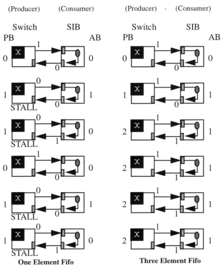
The worksheets "One Element Fifo" and "Three Element Fifo" help illustrate this principle. They show the state of the system after each cycle. The left boxes are a simplified version of the switch circuit. The right boxes are a simplified version of a SIB connected to a remote switch. The top arrow is the ValidIn bit, and the bottom arrow is the "Yunmy" line. The column of numbers underneath "PB" (perceived buffers) are the switch's conservative estimate of the number of ele-ments in the remote SIB at the beginning of the cycle. The column of numbers underneath "AB" (actual buff-ers) are the actual number of elements in the fifo at the beginning of the cycle.
The two figures model the "Balanced Producer-Consumer" problem, where the producer is capable of producing data every cycle, and the consumer is capable of consuming it every cycle. This would correspond to a stream of data running across the Raw tiles. Both figures show the cycle-by-cycle progress of the communication between a switch and its SIB.
We will explain the "One Element Fifo" figure so the reader can get an idea of how the worksheets work. In the first cycle, we can see that the switch is asserting its ValidOut line, sending a data value to the SIB. On the second cycle, the switch stalls because it knows that the Consumer has an element in its buffer, and may not have space if it sends a value. The ValidOut line is thus held low. Although it is not indicated in the dia-gram, the Consumer consumes the data value from the previous cycle. On the third cycle, the SIB asserts the YummyOut line, indicating that the value had been
con-(Producer) (Consumer) (Producer) . (Consumer)
Switch
PB
0S
0
0
STALL 0-0
STALLI
SIB
AB
0
1
0
0
00
0
1
0
STALL0
R=10STALL
One Element Fifo
sumed. However, the Switch does not receive this value until the next cycle. Because of this, the switch stalls for another cycle. On the fourth cycle, the switch finally knows that there is buffer space and sends the next value along. The fifth and sixth cycles are exactly like the sec-ond and third.
Thus, in the one element case, the static switch is stalling because it cannot guarantee that the receiver will have space. It unfortunately has to wait until it receives notification that the last word was consumed.
In the three element case, the static network and SIBs are able to achieve optimal throughput. The extra storage allows the sender to send up to three times before it hears back from the input buffer that the first value was consumed. It is not a coincidence that this is also the round trip latency from switch to SIB. In fact, if Raw were moved to a technology where it took multiple cycles to cross the pipelined interconnect between tiles (like for instance, for the Raw multi-chip system), the number of buffers would have to be increased to match
Switch
PB
SIB
0
0
0
1
0
2
22
2
Three Element Fifo
the new round trip latency. By looking at the diagram, you may think that perhaps two buffers is enough, since that is the maximum perceived element size. In actual-ity, the switch would have to stall on the third cycle because it perceives 2 elements, and is trying to send a third out before it received the first positive "Yummy-out" signal back.
The other case where it is important that the SIBs perform adequately is in the case where there is head-of-line blocking. In this instance, data is being streamed through a line of tiles, attaining the steady state, and then one of the tiles at the head becomes blocked. We want the SIB protocol to insure that the head tile, when unblocked, is capable of reading data at the maximum rate. In other words, the protocol should insure that no bubbles are formed later down the pipeline of producers and consumers. The "Three Element Fifo, continued" figure forms the basis of an inductive proof of this prop-erty.
Switch PB 2 2Z
2
2 2 3 STALL Switch AB PB 1 2 1 1STAL 1 STALL 1 0STALL 0 0 STALL0
J];_
1
3
E3
Switch AB PB AB 1 BLOCK 2 2 0 LOCK 1 01
S3
1 STALL O0 BLOCK3
BLOCK 1Three Element Fifo, continued
Starts at Steady State, then Head blocks (stalls) for four cycles I will elaborate on "Three Element Fifo,
contin-ued,"some more. In the first cycle, the "BLOCK" indi-cates that no value is read from the input buffer at the head of the line on that cycle. After one more BLOCKs, in cycle three, the switch behind the head of the line STALLs because it correctly believes that its consumer has run out of space. This stall continues for three more cycles, when the switch receives notice that a value has been dequeued from the head of the queue. These stalls
ripple down the chain of producers and consumers, all offsetted by two cycles.
It is likely that even more buffering will provide greater resistance to the performance effects of block-ages in the network. However, every element we add to the FIFO is an element that will have to be exposed for draining on a context switch. More simulation results could tell us if increased buffering is worthwhile.
2
r-4.0.3 Static Network Summary
The high order bit is that adding flow control to the network has resulted in a fair amount of additional com-plexity and architectural state. Additionally, it adds logic to the path from tile to tile, which could have perfor-mance implications. With that said, the buffering allows our compiler writers some room to breath, and gives us support for events with unpredictable timing.
4.1 THE SWITCH (SLAVE) PROCESSOR
The switch processor is responsible for controlling the tile's static crossbar. It has very little functionality --in some senses one might call it a "slave parallel move processor," since all it can do is move values between a small register file, its PC, and the static crossbar.
One of the main decisions that we made early on was whether or not the switch processor would exist at all. Currently, the switch processor is a separately sequenced entity which connects the main processor to the static network. The processor cannot access the static network without the slave processor's coopera-tion.
A serious alternative to the slave-processor approach would have been to have only the main pro-cessor, with a VLIW style processor word which also specified the routes for the crossbar. The diagram "The Unified Approach" shows an example instruction encoding. Evaluating the trade-offs of the unified and slave designs is difficult.
A clear disadvantage of the slave design is that it is more complicated. It is another processor design that we have to do, with its own instruction encoding for branches, jumps, procedure calls and moves for the reg-ister file. It also requires more bits to encode a given route.
The main annoyance is that the slave processor requires constant baby-sitting by the main processor. The main processor is responsible for loading and unloading the instruction memory of the switch on cache misses, and for storing away the PCs of the switch on a procedure call (since the switch has no local stor-age). Whenever the processor takes a conditional branches, it needs to forward the branch condition on to the slave processor. The compiler must make sure there is a branch instruction on the slave processor which will interpret that condition.
Since the communication between the main and slave processors is statically scheduled, it is very diffi-cult and slow to handle dynamic events. Context switches require the processor to freeze the switch, set the PC to an address which drains the register files into the processor, as well as any data outstanding on the switch ports.
The slave switch processor also makes it very diffi-cult to use the static network to talk to the off-chip net-work at dynamically chosen intervals, for instance, to read a value from a DRAM that is connected to the static network. This is because the main processor will have to freeze the switch, change the switch's PC, and
63 MIPS instruction 32 route instruction 0
op
E
rs rt imm IN IE IS IW P extraThe Unified Approach
63 48 32
1 op
I
rs rt imm MIPS Instruction63 48 32 26
op imm N