HAL Id: hal-00574379
https://hal.archives-ouvertes.fr/hal-00574379
Submitted on 8 Mar 2011
HAL is a multi-disciplinary open access
archive for the deposit and dissemination of sci-entific research documents, whether they are pub-lished or not. The documents may come from teaching and research institutions in France or abroad, or from public or private research centers.
L’archive ouverte pluridisciplinaire HAL, est destinée au dépôt et à la diffusion de documents scientifiques de niveau recherche, publiés ou non, émanant des établissements d’enseignement et de recherche français ou étrangers, des laboratoires publics ou privés.
Intrinsic defects and their influence on the chemical and
optical properties of TiO2x films
N Laidani, P Cheyssac, J Perrière, R Bartali, G Gottardi, I Luciu, V Micheli
To cite this version:
N Laidani, P Cheyssac, J Perrière, R Bartali, G Gottardi, et al.. Intrinsic defects and their influence on the chemical and optical properties of TiO2x films. Journal of Physics D: Applied Physics, IOP Publishing, 2010, 43 (48), pp.485402. �10.1088/0022-3727/43/48/485402�. �hal-00574379�
Intrinsic defects and their influence on the chemical and optical
properties of TiO
2-xfilms
N. Laidani1*, P. Cheyssac2, J. Perrière3, R. Bartali1, G. Gottardi1, I. Luciu1, 4and V. Micheli1
1
Fondazione Bruno Kessler, Via Sommarive, 18, 38123 Povo (Trento), Italy
2Laboratoire de Physique de la Matière Condensée (UMR CNRS 6622), Université de Nice Sophia-Antipolis, Parc Valrose, 06108 Nice cedex 2, France
3INSP, UMR 7188 CNRS Université Paris VI, 140 rue de Lourmel, 75015 Paris, France 4Dipartimento di Fisica, Università di Trento, Via Sommarive, 15, 38123 Trento (Povo), Italy * Corresponding author
ABSTRACT
In this work, TiO2 films produced by rf sputtering of a TiO2target, in argon and argon-oxygen plasmas were studied. The oxygen content in the feed gas was varied in a range of 3% – 20%. The chemical composition and structure of films were characterized by Rutherford backscattering spectrometry (RBS), X-ray photoelectron spectroscopy (XPS) and X-ray diffraction. Important information about the intrinsic defects of the films and their effects on the optical properties as well as a scheme of the energy band structure of the films could be derived from a combined use of optical spectroscopy and XPS.
Keywords: TiO2films, optical properties, electronic properties, defects, sputtering PACS: 68.55.ag; 68.55.Ln; 78.20.-e; 78.20.Ci; 78.40.-q; 81.05.Gc; 81.15.Cd
I- Introduction
Titanium oxide is an important material widely applied to many fields such as water electrolysis and photocatalysis [1,2] , photovoltaics where it is employed as the active part of the cells for solar energy conversion [3] and transparent conductive oxides for the production of transparent electrodes equivalent to those of indium tin oxide (ITO) [4-6]. The latter enters the structure of new generation solar cells, organic light emitting devices (OLEDs) and flat panel displays ; replacing ITO by a cheaper and more abundant TiO2 will lower the cost of devices. When doped with rare earth, TiO2can be used to increase the silicon-based solar cell
efficiency by modifying the solar radiation, through the conversion of high energy photons to other photons with a lower energy, more useful for silicon absorption [7,8].
A common feature unifies all these application fields, which is linked to the defects in TiO2
structure which strongly determine its electronic, electrical, optical properties and photo-activity. A great amount of work, mainly theoretical, has been done to investigate the nature, the energetics, the chemistry, the creation, the relaxation and the role of the defects states in
titania's band gap [9-14]. These studies treated the crystalline phases, bulk rutile or anatase, of TiO2, but very few works have been reported on defect peculiarities in titanium oxide films. In this work, a joint study was conducted to determine the relevant optical, electronic and defect properties of thin TiO2-x films produced by RF sputtering of a TiO2target. Density and
stoichiometry of films deposited in various Ar-O2 mixtures and plasma conditions were
derived from x-ray photoelectron spectroscopy (XPS), Rutherford backscattering spectrometry (RBS). The different phases of TiO2 were determined using X-ray diffraction
(XRD). The films reflectance spectra have been measured in the visible range. The optical indices and energy gap of the material have been extracted; their interpretation allowed to define an energy band scheme and the gap states.
II- Experimental details II.1 The sample preparation
A series of films has been prepared by RF sputtering under a self-bias voltage at cathode and at a 2 Pa pressure. A TiO2disk with 10 cm diameter from Goodfellow was used as target. The
samples were at floating potential and were not externally heated. The sputtering gas was oxygen-containing argon. Various conditions of process were applied and are summarized in Table 1: oxygen content in argon varied from 0 to 20 vol. % and self-bias voltages at the target were -550 V and -750V; films are consequently labeled.
Films were deposited onto n-doped silicon (100) and 1mm thick glass substrates; their mechanical thicknesses have been determined with a stylus profilometer and serve as starting data in the optical constants calculations. The measured film thicknesses are given in Table 1.
I1.2 The sample characterization a- RBS
The film composition has been determined by RBS, using a 2 MeV Van de Graaff accelerator. The oxygen content was determined with a 5% accuracy, due to the low RBS yield for light elements like oxygen.
b- XPS
Films were analyzed with a Scienta instrument, with AlKα radiation (1486,6 eV). Both core levels and valence band spectra were acquired. All binding energies are given with respect to Fermi level (EF).
The chemical composition and oxide stoichiometry of the films surface were derived from XPS analysis by applying Scienta sensitivity factors for the core levels. The position of EF
with respect to the valence band maximum (VBM), and states in the gap below EF, were
determined from analysis of the valence band spectra. A bulk rutile sample from Goodfellow was used as a reference bulk material for the TiO2films. No special surface treatment such as
ion etching in the analysis apparatus was carried out for rutile or the films. An electron flood gun was used to compensate the accumulation of surface electrostatic charge onto the samples during analysis. Two runs of measurement were made on each film and five on rutile.
c- UV-Visible optical spectrophotometry
Optical reflectance measurements were made on films deposited on glass substrates, with a Jasco V-550 spectrophotometer in the 300–900 nm wavelength range. Calibration has been realized with sapphire, a material whose refractive index is the order of the sample's one, in order to assess the experimental measurement error, which was found as 0.5%. Care was taken to absorb any possible reflected beam from the rear face of sapphire or substrates by a black carbon strip in order to avoid any back-reflected wave. Reflectance spectra Rexpwere
recorded in the visible range, at normal incidence.
d- XRD
The phase structure of the films was determined by using a Seeman-Bohlin (grazing angle configuration) X-ray diffractometer with Cu Kαradiation at an incident angle of 3°, in steps of 0.02°.
III- Results and discussion
III.1- Film composition and density from RBS analysis and correlation with deposition rate: All films can be described as TiO2-x and their composition was obtained by RBS. Table 1
reports the O/Ti atomic ratio given by RBS. The films with the higher O/Ti value are those grown in pure argon plasma, the O/Ti reaches a flat regime when oxygen concentration in the gas is higher than 10%.
The measured film thickness and the number of atoms per cm2 unit surface allow the calculation of the atomic density of films. For the F10(1) and F20(1) films however, the relative
errors of thickness measurement, 13% and 20% respectively, were too high, then we have used the thickness given by the simulations of the optical reflectance and given in Table 1.
Fig.1 shows the atomic density of films: clearly, films F0(1) and F0(2) grown in pure argon
plasma have the higher density. The decrease in density when adding O2to Ar in the feed gas appears more evident for films grown with a -550 V cathode self-bias voltage (group Fi(1),
i=3,10,20 in Table 1). The lowest value was found for film F20(1), a value ~30% lower than
the nominal value of rutile.
The variation of the film density with both the cathode voltage and the oxygen concentration in the gas can be understood by also considering the variation of the film deposition rate. This parameter is plotted in Fig.1(b). As expected, the higher the voltage, the higher the rate. As can also be seen, O2 introduction resulted in a less efficient sputtering process owing to the
fact that the partial pressure of Ar was lowered upon O2 addition in the gas, which decreased
Ar+ion density in the plasma too.
Globally, the voltage conditions at the cathode which led to higher deposition rates led also to higher film density. However, as said above, within a film series deposited at a same cathode voltage, film density varied strongly with O2concentration in the gas mixture. This result is to
be more likely correlated with the energetic conditions at the substrate. The density decrease obtained when O2 was added can reasonably be explained by a more open structure due to
less efficient interaction between the growing film and the most energetic species of the plasma. Plasma-surface interaction through ion bombardment is known to increase surface mobility of the impinging atoms on the substrate or on the growing film surface, leading to film densification.
III.2- Chemical states and film surface stoichiometry from XPS analysis
The XPS analyses regarded all of core levels Ti2p, O1s and valence band spectral regions. Carbon core level spectrum was also acquired. Carbon stems from surface hydrocarbon contaminants, it also serves as a reference to correct the binding energy (BE) shift due to surface electrostatic charging, either under flood electron gun application or without. The C1s spectrum has been set at 285 eV, the same shift has been applied to scale all BE spectra discussed below.
Fig.2 (a) displays the Ti2p core level spectrum related to bulk rutile. It consists of Ti2p3/2and
Ti2p1/2 contributions located at 458,35 eV and 464,02 eV respectively. The peaks are
well-fitted with symmetric gaussian-lorentzians. The Ti2p3/2 BE agrees well with published data for Ti4+states in TiO2 (458,7 eV in [9] and references therein for example).
The corresponding O1s displayed in Fig.3 (a) is dominated by a peak at 529,75 eV, i.e. 71.40 eV higher than that of Ti2p3/2. This corresponds well to oxygen O1s BE in titanium oxide [15,16]. This spectrum can be fitted with four peaks: the major one OI pertaining to O2- ions
in titanium oxide and the others at 531,01 eV (OII), 532,01 eV (OIII) and 533,06 eV (OIV). The
atomic ratio OI/Ti, deduced from Ti2p3/2 and OIpeak areas, is equal to 1,90 (±0,03).
The missing oxygen with respect to the ideal formula of the oxide TiO2, could be at the origin of the OII contribution. In fact, in many transition metals hydroxylation gives rise to a peak
whose energy is close to the OIIpeak one [17,18], due to metal-OH bond formation. However,
O atoms giving rise to OIIpeak are in a ratio with Ti atoms (OII/Ti) of 0,62 (± 0,01): this is
much higher than the oxygen deficiency x = 0,1 in the present stoichiometry (TiO1,9) with
respect to ideal TiO2. The OIIpeak more likely stems also from oxygen bonded to carbon like
in C-OH [19], masking any Ti-OH contribution to the present O1s spectrum.
As for the remaining peaks resulting from the spectrum fitting, peak OIII and OIV, they have
been reported to pertain to either adsorbed molecular H2O [20, 21] or C-O bondings like O-C-O or O-C-O=C-O-C-O [19].
Fig.2 (b and c) shows the Ti2p core level spectra related to films F0(1) and F10(1). With
respect to that of rutile, Ti2p3/2 BE are slightly up-shifted respectively to 458,83 and 458,80
eV. This shift is also observed in the O1s spectra (Fig. 3 (b and c)). Actually, such a shift towards higher energies were observed for all films. However, the difference between Ti2p3/2 and OIpeak BEs remains constant as 71,43 ± 0.02 eV and equal to that of rutile: this indicates
that the chemical states of Ti and O are the same in these films and in rutile. The BE shift observed in the spectra is only related to a variation of EFwith respect to the core lines, due to
band bending caused by a non-zero surface potential during the analysis. Indeed, dealing with semi-conductors materials, band bending is expected in presence of a non-zero surface potential. We verified this effect in the case of rutile. Various spectra were measured under different electron beam energy conditions used for surface charge compensation, which create different sample surface potentials. The latter are reflected in different binding energy shift corrections for misaligned sample and spectrometer Fermi levels. After correction for surface charging, Ti2p and O1s binding energy are given in Table 2; they depend clearly on the energy of the incident electron beam under which the spectra were measured.
The OI /Ti atomic ratios deduced from Ti2p3/2 and OIpeak areas obtained for all films are
displayed in Table 1. Contrarily to O/Ti values from RBS analysis, no clear trend is observed in the variation of the OI/Ti ratio values with the oxygen concentration in the sputtering gas.
As can be seen, all films are under-stoichiometric. As the XPS-derived OI /Ti atomic ratio
regards oxygen in Ti-O-Ti bonds only, the observed deviation “x” in these TiO2-x films from
the ideal stoichiometry TiO2 can be due to structural defects as O vacancies, either unhealed or healed by H2O adsorption giving Ti-OH bonds [22]. Similarly to rutile, the latter cannot be
quantified as they are masked by C-O bonds in the OII peak in O1s spectrum. In fact, the
OII/Ti atomic ratio is, again as for rutile, in all cases much higher than “x” in these TiO2-x
films (Table I).
III.3- Valence band maximum energy
In rutile, Ti atoms are surrounded by six oxygen atoms, forming a distorted octahedron. Due to crystal field, the Ti3d orbitals split into two sets of orbitals, eggrouping dz2and dx2-y2and
t2g, grouping dxy, dxz and dyz. Oxygen atoms are surrounded by three Ti atoms in a planar
geometry. sp2hybridisation of O atoms forms threeσbonds (from px, pyand s orbitals) in the
plane and one π bond (from pz) perpendicularly to the plane. The valence band (VB)
spectrum reflects the density of filled states, weighted by the photoemission cross-section. The top of VB of TiO2is occupied by O2p non-bonding states. The egstates of Ti 3d orbitals
are bonded in σ orbitals and are located in the lower energy region of the VB, while the t2g
states are bonded inπorbitals and lye higher in energy than theσstates, midway between the σ states and the O2p non-bonding states [23]. A VB spectrum is displayed in Fig. 4(a) for F20(1), where the different spectral regions are indicated. For comparison, a fit of the VB
spectrum of rutile is also shown in Fig. 4(b). Differences between the two spectra can be observed, in particular in the lowest and in the highest energy sides of the spectra. The assignment of such peaks is given in the following sections.
The valence band maximum energy (VBM) is determined as the zero intensity energy of the low BE region of the spectrum. After a Shirley background subtraction, the VBM energy is found by extrapolating a linear fit of the final spectrum portion to zero-intensity (inset in Fig. 4(a). The obtained values are reported in Table 2, for the films and the rutile reference. For the latter, only a mean value is given.
III.4- Chemical states above the VBM
The valence band, as described above, did not sign the upper end of the XP spectrum below Fermi level for all the samples. Between VBM and the Fermi level, a low intensity peak can
be measured, as can be seen in Fig. 4(a) and in the inset therein; its position is given in Table 2 , together with its area ratio to the Ti2p3/2peak.
Neither rutile nor film F0(1) spectrum exhibited such a peak, while for all the other films the
ratio of this peak to Ti2p3/2 peak varied between 3x10⁻⁴ to 8x10⁻⁴. This feature has been
reported for under-stoichiometric titanium oxide. It has been assigned to Ti3d states and attributed to oxygen vacancies which result in partially filled Ti3d nonbonding states in the gap [9, 24, 25, 26]. It has been also shown that other defect states like interstitial Ti can give rise to a similar state between the VBM and Fermi level [14].
The area ratio between this gap state peak and Ti2p3/2 was calculated and it is shown in Fig.
5(a) in function of the measured OI/Ti atomic ratio. It appears that the relative quantity of the
Ti3d states detected above the VBM doesn’t follow the deviation “x” from ideal stoichiometry of the oxide as obtained by XPS, as it should if these states were due to oxygen vacancies. Here, the closer the OI/Ti ratio value to 2, the higher the Ti3d/Ti. In our
assumption that the lacking O atoms to form stoichiometric TiO2are either O vacancies or O
atoms involved in Ti-OH bonds which do not contribute to OI peak, O vacancies cannot
explain the evolution of Ti3d/Ti in Fig. 5(a) as the higher their number, the more intense should be the Ti3d peak. On the contrary, films with more hydroxylated Ti (i. e. lower OI/Ti
ratio value) as a result of O vacancy healing, should give a lower Ti3d/Ti ratio. This can account for the dependence between the OI/Ti and Ti3d gap states of Fig. 5(a). It is then likely
that in regions of the surface sampled by XPS, O vacancies are healed in the form of Ti-OH bonds by dissociation of foreign H2O molecules from ambient.
A fingerprint of hydroxyl groups bonded to Ti can be found in the VB spectra. Ti-OH bonds give a peak at the bottom of this spectrum, at ~11 eV of BE, corresponding to the3σ orbital of the OH radical [27, 28]. This peak, indicated in Fig.4(a-b), was observed for all the film and rutile spectra. In Fig. 5(b) its relative area with respect to the VB spectrum is plotted in function of the Ti3d/Ti area ratio. The dependence of the Ti 3d sites on the hydroxyl groups number and the healing effect of the latter on the defects is clear.
In contrast with the above XPS analysis which samples the outermost surface layers, RBS gives information about the film composition in its whole volume. Interestingly, the Ti3d/ Ti2p3/2 area ratio determined by XPS correlates well with the oxide stoichiometry given by
RBS. Fig. 5 (c) shows clearly that the highest relative Ti3d states concentrations are obtained for the lowest O/Ti ratio. On one hand, this result would corroborate the attribution of the Ti3d states origin below Fermi level to O vacancies and, on the other hand, the relationship
between Ti3d/Ti and OH3σ/VB area ratios indicates that the hydroxyl bonds are not confined at the topmost surface layers but are distributed also in the film volume.
III.5- Film structure from XRD analysis
X-ray diffraction analysis for films grown in pure argon plasma showed either a featureless spectrum, indicating an amorphous structure, or a typical peak, though of very weak intensity, of rutile nanoparticles. The spectra obtained with oxygen addition to argon gave both rutile and anatase diffraction patterns, whatever the oxygen concentration in the gas and the cathode voltage. The spectra relative to F0(1) and F20(1) films are displayed in Fig. 6 (a) and (b)
respectively, as representative of the case of Ar and Ar-O2 plasmas (F0(2) film appeared
amorphous in these analyses, spectrum not shown). The rutile structure is signed by the (110) peak and anatase is by the (101) diffraction peak.
III.6 - Optical properties from reflectance measurements: complex refractive index and optical gap
Possible gap states above the Fermi level due to O vacancies are not detected by XPS. Optical measurements performed on the films under study were of great help in determining both the fundamental gap of the films and the existence of extrinsic gaps due to defect states and to defining a band energy scheme of the films.
III.6.1- Film complex refractive index
A series of five films, F0,10,20 (1) and F0,20 (2), has been studied. Their reflectance spectra
Rexp(λ) are shown in Fig. 7(a); for clarity, spectra of films F0,10,20 (1) are up-shifted
respectively by 0.28, 0.6 and 0.65. Here, one intends to simulate the shapes of the various spectra and mainly get the refractive and absorption indices of the films and the energy gap of the material. Transmittance measurements (not reported here) have been performed and have showed that absorption exists to a small extent in our films; reflectance spectra Rexpwere used in order to extract a thickness “d” and the indices in which absorption is taken into account. The thickest films F0(2) and F20(2) clearly exhibit interferences; then, even if absorption
exists, it should remain small but not negligible if one intends to fit calculated and experimental spectra to extract the film complex index n (λ) = ν(λ) + iκ(λ) or its complex dielectric function ε(λ) =ε1(λ) +iε2(λ).
A classical relation [29] gives the theoretical expression of Fresnel reflectance R of a film deposited onto a substrate: RFresnel=ρρ* where
ρ
=ρ
12 +ρ
23 e 2 ikd1 +
ρ
12ρ
23 e2 ikd (1)
k is the wave vector inside the film, ρ12is the vacuum-film reflection coefficient,ρ23that of
the film-substrate interface.
A multi-step calculation procedure was applied in order to determine starting data with a good approximation, which consisted in successively using the following models:
- Sellmeier and Wemple-Didomenico (W) [30] models; the latter expresses ν(λ)in the transparency domain of the material but recalling absorption explicitly through a measure of the strength of interband optical transitions (Ed) and the single oscillator
energy associated with the maximum of absorption (E0): νW
2 =
1+ E0Ed E02−E2
- Forouhi-Bloomer (F-B) model to calculate κF−B(λ) [31], which, used withνW(λ) previously estimated, served as entry data for reflectance simulation; F-B’model leads
to first values of the energy gap Eg: κF−B =
A'(E−Eg)2 E2−B' E+C'
- Ketteler-Helmholtz model (K-H), based on the complex dielectric function and in which transparency and absorption domains are consistently taken into account. In contrast with what was done in the previous steps, within K-H model the real and imaginary part of the dielectric function are determined simultaneously. d, νW(λ),
κF−B(λ) and Eg determined above served as input data in order to determine νK−H(λ) and κK−H(λ) which were the final values of these calculations.
The substrate index has been determined first (the calculations are given in Appendix A). Each step of the film reflectance simulation is described in more details in appendix B.
Fits between Rexpand RFresnel were performed and, in the following, we give the final results
of the calculations. Fig.7(b) shows the agreement that has been obtained by our simulations between R exp and RFresnel for film F0(2) and ν(λ) and κ(λ) are given in Fig. 8 (a) and (b)
respectively. What can be noticed is that ν(λ)varies significantly among the various samples. In order to better illustrate this result, the real part ν(λ)of n (λ) corresponding to λ = 632,8 nm (i.e. the He-Ne laser wavelength commonly used for ellipsometry) is plotted in Fig. 9 in function of the atomic ratios O/Ti from RBS (plot a) and OI/Ti from XPS (plot b). Except for
F10(1) (not represented), all the points are fairly aligned in Fig.9(a) following a decreasing
linear function with O/Ti from RBS. By considering the relationship between this ratio and the Ti3d states relative amount (Fig.5(c)) and between the amount of the Ti3d states and OH states (Fig. 5(b)), the effect of hydroxylation on ν(λ) value become clear. This is also what can be observed in Fig. 9(b): ν(λ) increases with OI/Ti from XPS. So, in determining the
film refractive index values is the extent to which water interacts with the films. This can be due to the film internal structure itself as a low refractive index is usually related to a low packing density of the film grains or columns. With a high melting point material like titanium oxide (1867°C), films grown at room temperature as the present ones are more likely of a columnar structure [32]. The surface area of the columns can affect strongly the refractive index values [33]. On the other hand, for these films, crystallisation can also be a factor of the higher values of refractive index of the films grown in presence of oxygen [34, 35]: XRD analysis revealed an amorphous state or weak crystallinity of the films deposited in a pure Ar plasma while a stronger crystallinity (though at nanoscale) was observed in all films grown in Ar-O2plasma, as shown in Fig. 6. Correspondingly, theν(632,8 nm) values of F0(1) and F0(2)
are lower than those ofF20(1)and F20(2). The variations of the refractive index of the present
films appear to be determined by both crystallinity and packing density which, in turn, determines the hydroxylation extent.
Finally, the imaginary partκ(λ) of n(λ) has been used to determine the optical band gap of the films, this is discussed in the next section.
III.6.2 - Film optical gap fromκΚ−Η(λ)and gap states:
The optical band gap can be determined from the absorption coefficient α = 4πκ/λ.Tauc model [36] describesαin the high absorbance region of the wavelength range as:
αE = A (E – Eg)γ (2)
where E is the incident photon energy, Eg is the energy gap, A a constant independent of E andγhas four possible numeric values: 1/2, 2, 3, 3/2. Generally an ad hoc assumption is made of a kind of transition (direct allowed when γ=1/2, indirect allowed when γ =2, indirect forbidden for γ =3 and direct forbidden for γ =3/2) and the (αE)1/γ versus E curve is fitted with a linear function.
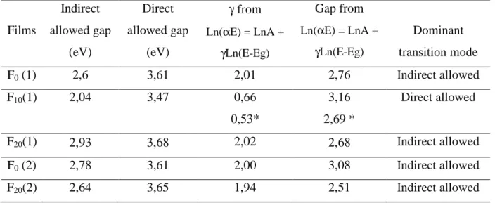
(αE)1/2=A(E-Eg) and (αE)2=A(E-Eg) were plotted versus E in order to derive a direct and
indirect allowed gap, which values are reported in Table 3. As it can be seen, the values for the direct allowed transitions are higher than for bulk TiO2which direct allowed gap can be of
3,3 – 3,4 eV [37]. This can be related to amorphicity or to a quantum size effect due to a nano-crystallinity in the film structure.
On the contrary, the Eg energy values corresponding to an indirect allowed transition resulted
lower (between 2,04 and 2,93) than what reported in literature for titanium oxide (3,02 – 3,19 eV respectively) [37]. This light absorption is unlikely to pertain to the intrinsic band structure of the films, but rather to absorption by intrinsic defects. In order to check the existence of such a transition mode, no a priori assumption was made for theγvalue in Eq. 2, rather theαE versus E curve is fitted following:
Ln(αE) = LnA +γLn(E-Eg) (3)
The Egvalue as well asγvalue are obtained as curve fit results. In the inset of Fig. 8(b) such a
curve fit is shown for film F20(1) for photon energies ≥ 3,5 eV. The fit results regarding Eg
and γ are summarized in Table 3 for all the films. This method allowed to identify the dominant transition mode in the photon energy range under study. In the case of F10(1), γ =
0,66 indicating rather a direct allowed transition and confirming that for E ≥ 3,5 eV, the intrinsic gap is direct. For all other films, we can see that γ is close to 2. No value of γ representative of a forbidden direct or indirect transition resulted from the fit following Eq. 3. So, only the allowed transitions are likely to occur. All the energies fall in the visible range. For F10(1), a second gap value of 2,69 eV could be found by fitting Ln(αE) following Eq. 3for
E <3,5 eV, far from the fundamental gap energy region.
Light absorption in the visible can, in fact, be due to lattice defects which create energy levels within the gap of titanium oxide: defects in the oxygen sub-lattice related to O vacancies and those related to Tin+ (n=3 or/and 2) ions. Although literature is abundant for the electronic structure of titanium oxide, many recent papers recognize that there still exists insufficient information on the optical properties of point defects. In a review made by Kuznetsov and Serpone [38], the absorption bands in the visible spectral region are reported to be associated to O vacancies, which act as F-type color centers in a range of 2,93- 2 eV. In this case, light absorption can originate from transitions between the defect-induced energy levels inside the gap and the Ti3d levels in the conduction band (CB). Let’s recall that there are three types of the F-type centers: doubly-ionized and optically silent O vacancies (the so-called F++centers), O vacancy with one trapped electron (F+-center) and with two trapped electrons (F-center). In turn, Chen et al. attributed an absorption energy of 1,78 eV for transitions between a F+-center and CB, and one of 0,87 eV for transition involving a F-center and 0,20 eV for a F++-center [39].
For our films, the extrinsic absorption energy values found so far fall in the interval 2,60 – 2,78 eV as it can be seen in Table 3, corresponding to wavelengths between 446 – 470 nm. Such a set of values could be F- and F+- centers related to O vacancies [40], although no unambiguous identification can be made.
Moreover, at variance with the other films, the film F10(1) shows an increase ofκ(λ) beyond
~850 nm (below ~1,45 eV). The trend ofκ(λ)in this region clearly indicates absorption in the near infra-red which could be associated with Ti3+-related centers (Ti3+ in substitutional or interstitial sites) [38, 40].
III.7- Electronic band structure scheme:
In order to define a band structure of the various films of this study, optical results were used in conjunction with XPS analysis of the valence band. In Fig. 10, a schematic representation of the band structure is given, which shows the VBM energy, the conduction band minimum (CBM) and the gap states, all referred to the Ti2p3/2 BE. This reference level of energy was
chosen in order to get rid of band bending effects due to surface states.
It can be seen that in the films the band edges move with respect to that of rutile, there is a recession of the VBM, probably due to the disappearance of states at the top of the band in relation with the oxygen deficiency. As for the intermediate states inside the gap, two extreme cases can be assumed concerning their positioning on the energy scale: the transitions occur between the VBM and the color center level (Fig.10(a)) or between the center level and the CBM (Fig. 10(b)). The first case would place the defect related level above the Ti3d states while, in the second one, it would be between the Ti3d states and the VBM. The latter case is unlikely because no significant peak was observed in that region of the films XP spectra. Besides, in Fig. 10(a), the energy difference δbetween the color center level and CBM is reported. The values are close to those of Chen et al [39] for F-color center absorption in rutile, i.e. O vacancies with two trapped electrons.
IV- Summary
In this study, TiO2-x films were deposited by RF sputtering in Ar-O2 mixtures at room
temperature. Emphasis was put on the structural and optical properties of the films in order to define a method based on a combined use of x-ray photoelectron and optical reflectance spectroscopies. The intrinsic defects were also studied in conjunction with RBS analysis and a scheme of the energy band structure of the films was proposed.
In order to quantify optical behaviour, the experimental reflectance spectra were fitted within the frame of a multi-step procedure using different models. This approach was necessary to rigorously derive the film optical constants for a spectral region where absorbance cannot be totally neglected in spite of a high transparency.
The following conclusions were drawn from this study:
(1) All the films were oxygen-deficient and adding oxygen to the sputtering gas was found to further increase the deviation from a full stoichiometry.
(2) The reduced oxide state in the films induced states related to O-vacancies between the VBM and the Fermi level which were strongly correlated with hydroxylation.
(3) Hydroxylation did not appear confined to the surface layers but concerns the film volume as well and had an effect on the refractive index.
(3) O-vacancies made band edges recede, due to energy states disappearance from the top of the VB.
(4) Intermediate bands inside the fundamental gap were likely due to the F-centers.
Acknowledgements:
The financial support of the “Fondazione Caritro” (Trento) in the frame of Oxi-Solar project is gratefully acknowledged.
N.L. thanks Nice Sophia-Antipolis University for the support of her stay at “Laboratoire de Physique de la Matière Condensée”.
Appendix A: Index of the substrate
The rear face of the substrate being blackened, its reflectance is expressed by
Rs=
ns−1 ns+1
2
and does not show interference fringes. The substrate index ns(λ) is involved in
the relations that express the reflectance of the film deposited onto its substrate and it must be known prior to the interpretation of optical spectra of TiO2films. ns(λ) has been developed in
series ns2=a0+a1 λ + a2 λ2 + a3 λ3 + a4
λ4 and limited to the fourth order in λ, no gain being added
with higher orders. From Rs, one extracts ns (λ). The ai's are determined by a least square
procedure which gave a0 =2,248, a1 =−16,7nm, a2=41617nm2, a3= −5518400nm3 and a4 = −43112nm4.
Appendix B: Film optical parameters calculations from reflectance spectra B.1 First step: calculation ofν(λ)
Absorption is neglected; a Sellmeier model of bulk TiO2 index n (λ), valid for λ > 430 nm [41], gives ' ' ' ' ' ) ( 2 2 2 2 2 e d c b a n − + − + = λ λ λ λ λ (4)
This allows to obtain an order of magnitude of n (λ) by a simple mean.
In the transparency domain and within Wemple-Didomenico model (W) [30], the real part
νW 2 of n (λ) can be transformed as νW 2 (λ)=1+ λ0W λDW λ2 λ2−λ 0W 2 (5)
The authors give Ed = 25,7 eV which corresponds to λDW ≈48,11nm and E0 = 5,24 eV corresponds to λ0W ≈236nm , then 0 =4,0548
DW W λ
λ
. For TiO2, Eq.5 is valid forλ>λgap.
Remark that, for λ = 550nm, c'≈22,44 and 0,0026
' ' 2 2 ≈ −e d λ λ
; then Eq.5 is formally
equivalent to Eq.4 if one neglects the third term in the latter and let a'≈1,
DW W b λ λ0 '≈ and W c'≈λ20 .
The “optical” thickness d has been determined for each film. Actually, Wemple's model describes the properties of the "red part" of TiO2 optical spectrum. An agreement between calculated and experimental spectra that reproduces their general shape while fitting the "red peak" is obtained with the values given in Table 1. These thicknesses will be used whatever the model for absorption.
B.2 Second step: calculation of κF−B(λ)
As derived from W simulations, an absorption band exists at λ0W ≈236nm . Sellmeier
and W models assume that the absorption band would be far enough for its influence to be negligible. In the various simulations of Rexp, we found that one could not consider that this
was the case. Actually, λ0W is close to the wavelength range under study and is responsible for the difficulties encountered along the index solving procedure. This absorption band has been taken into account with F-B [31] formalism given in Section III.6.1. Once the extinction
coefficient κF−B(λ) is introduced in n (λ), Eq. 5 must be slightly modified, since the numerical values ofν(λ) that have led toνW(λ) were obtained assuming thatκ(λ) = 0. More generally, Eq. 5 writes
νW 2 ≈A+ ∆ λ 2 λ2−λ 0 2 (6)
The magnitude of A remains small compared to that of the second term, and so does its influence in the simulations. Using κF−B(λ) expression and Eq. 6, and entry data Α≈1,
9 , 4 0 ≈ = ∆ D λ λ
, the simulation gives κF−B(λ) that realize the best fit between Rexpand RFresnel.
In Rexpsimulations,λ0is found to influence the position of extrema in the blue part of spectra;
for our series of samples, the best fit occurs when the mean value < λ0> ≈ 231,8± 3,0 nm, very close to λ0W ≈236nm already published [30].
B.3 Application of the Ketteler-Helmholtz model
A set of thicknesses, indices and energy gaps has been estimated through the previous simulations. They serve as entry data for Ketteler-Helmholtz model, in which the real and imaginary part of the dielectric function are determined simultaneously, in contrast with what was done in the previous steps.
The absorption band recognized before is unique in the range under study; the real and imaginary parts of the complex dielectric function ε (λ) of TiO2are recalled in Eq. 7 and 8.
) ( ) ( ) ( ) ( ) ( 1 2 2 2 0 2 2 0 2 2 0 2 2 1 ν λ κ λ λλ λ λ λ λ λ ε −K−H = K−H − K−H Γ + − − ∆ + = (7) and ) ( ) ( 2 ) ( ) ( 2 02 2 0 2 0 3 2 ν λ κ λ λλ λ λ λ λ ε = Γ + − Γ ∆ = − −K H (8) where 02 02 2 2π λ ϕ λ ω = = ∆ c p and Γ = 1 2πcτ λ0 =β λ0
Approximate values of a few parameters that enter K-H's relations have been determined according to the following arguments.
- We assume that far from the absorption band, i.e. in the red part of spectra, all models should give more or less the same results. When Γλλ0<<λ2−λ02 and simultaneously ε2 <<
ε1−K−H ≈νW
2
and get approximate input values of ∆, λ0 and Γ. A first run uses Eq. 7 and 8,
simulates Rexp and gives an approximation of ε1−K−H(λ) and ε2−K−H(λ). A first value of λ0−K−H comes then from ε1−1=0.
- The end of the whole process described above comes from a few remarks:
From the previous run, the numerical ratio ε1−1 ε2
can be drawn; it gives a rather linear
behaviour (not shown) as a function of λ, that is expressed by ε1−1 ε2
≈uλ+v. At this stage, one gets a new value of λ0K−H ≈ −u
v from a full K-H treatment, although not yet the most accurate one. In the last run of the simulation, we use the theoretical ratio
ε1−1 ε2 =β−1λ 2−λ2 0−K−H λλ2 0−K−H
of Eq.7 / Eq.8, and β−1 is expanded as a polynomial function of λ.The fit is improved especially in the spectral zone [300-400] nm where absorption is important.
Fits for all films have led to the absorption band located at aλ0 with a mean value <λ0K−H> = (238,2 ± 3,1) nm.
References
[1] Akira Fujishima, Xintong Zhang, Donald A. Tryk, Surface Science Reports 63 (2008) 515
[2] K. Yamaguti, S. Sato, J. Chem. Soc. Faraday Trans. I 81 (1985) 1237
[3] M. Grätzel, Nature 414 (2001) 338; M. Grätzel, J. Photochem. Photobiol. C 4 (2003) 145. [4] Chiu, N. Kikuchi, Appl.Surf. Sci. 255 (2009) 9695
[5] L.R. Sheppard, T. Bak, J. Nowotny, M.K. Nowotny, International Journal of Hydrogen Energy 32 (2007) 2660 – 2663
[6] Yasushi Sato, Hideo Akizuki, Toshihisa Kamiyama, Yuzo Shigesato, Thin Solid Films 516 (2008) 5758–5762
[7] B.S. Richards, Solar Energy Materials & Solar Cells 90 (2006) 1189
[8] C. Strümpel, M. McCann, G. Beaucarne, V. Arkhipov, A. Slaoui, V. Švrc ek, C. del Ca izo, I. Tobias, Solar Energy Materials & Solar Cells 91 (2007) 238
[10] M. Veronica Ganduglia-Pirovano, Alexander Hofmann, Joachim Sauer, Surface Science Reports 62 (2007) 219–270
[11] X. Li, M. W. Finnis, J. He, R. K. Behera, S. R. Phillpot, S. B. Sinnot, E. C. Dickey, Acta Materialia 57 (2009) 5882
[12] J. Nowotny, T. Bak, M. K. Nowotny, L. R. Sheppard, International Journal of Hydrogen Energy 32 (2007) 2630
[13] T. Bak, J. Nowotny, M. Rekas, C. C. Sorrell, J. of Physics and Chemistry of Solids 64 (2003) 1057
[14] S. Wendt, P. T. Sprunger, E. Lira, G. K. H. Madsen, Z. Li, J. Ø. Hansen, J. Matthiesen, A. Blekinge-Rasmussen, E. 15 Lægsgaard, B. Hammer, F. Besenbacher, Science 320 (2008) 1755
[15] J. Jun, J-H. Shin, M. Dhayal, Appl. Surf. Sci. 252 (2006) 3871
[16] J. F. Moulder, W. F. Stickle, P. E. Sobol, K. D. Bomber, “Handbook of X-ray Photoelectron Spectroscopy”, ( J. Chastaing, R. C. King Jr., Eds., Physical Electronics, Inc. Eden Prairie, 1995)
[17] T. L. Barr, J. Phys. Chem. 82 (16) (1978) 1801
[18] H. M. Liao, R. N. S. Sodhi, T. W. Coyle, J. Vac. Sci. Technol. A 11(5) (1993) 2681 [19] G. Beamson and D. Briggs, “High Resolution XPS of Oraganic Polymers, The Scienta ESCA300 Database”, (John Wiley &Sons, West Sussex, 1992)
[20] D. Costa - P. Marcus - W.P. Yang, Journal Electrochem. Soc., Vol 141, N°10, 2669 [21] H.P. Marques, A.R. Canario, A.M.C. Moutinho, O.M.N.D. Teodoro, Applied Surface Science 255 (2009) 7389
[22] L.-M. Liu, P. Crawford, P. Hu, Progress In Surface Science 84 (2009) 155 [23] D. W. Fisher, Phys. Rev. B5 (1972) 4219
[24] C. Di Valentin, G. Pacchioni, A. Selloni, Phys. Rev. Lett. 97 (2006) 166803
[25] L. Fleming, C. C. Fulton, G. Lucovsky, J. E. Rowe, M. D. Ulrich, J. Lüning, J. Appl. Phys. 102 (2007) 033707
[26] T. L. Thompson, J. T. Yates, Chem. Rev. 106 (2006) 4428
[27] S. Eriksen, P. D. Naylor and R. G. Egdell, Spectrochimica Acta 43A (1987) 1535 [28] E. V. Stefanovich, T. N. Truong, Chem. Phys. Lett. 299 (1999) 623
[29] Born, E. Wolf, " Principles of Optics", (7thed., Cambridge University Press, Cambridge, MA, 1999)
[30] S.H. Wemple, M. Didomenico, Phys. Rev. B 3, (1971) 1338 [31] A. R. Forouhi and I. Bloomer, Phys. Rev. B 34 (10) (1986) 7018
[32] Thornton JA, Hoffman DW. Thin Solid Films 5 (1989) 171
[33] M. Harris, M. Bowden and H. A. Macleod, Optics Communications 51 (1) (1984) 29 [34] A. H. Yuwono, B. Liu, J. Xue, J. Wang, H. I. Elim, W. Ji, Y. Lic and T. J. White, J. Mater. Chem. 14 (2004) 2978
[35] M. M. Hasan, A. S. M. A. Haseeb, R. Saidur, and H. H. Masjuki, International Journal of Chemical and Biological Engineering 1(2) (2008) 92
[36] J. Tauc, R. Grigorovici, A. Vancu, Phys. Status Solidi 15 (1966) 627 [37] N. Daude, C. Gout, C. Jouanin, Phys. Rev. B15 (6) (1977)3229 [38] V. N. Kuznetsov, N. Serpone, J. Phys. Chem. 113 (2009) 15110 [39] J. Chen, L.-B. Lin, F.-Q. Jing, J. Phys. Chem. Solids 62 (2001) 1257 [40] N. Serpone, J. Phys. Chem. B 110(48) (2006) 24287
[41] E.D.Palik (Ed.), “Handbook of Optical Constants of Solids” (Academic Press, New York, 1985)
Table 1: Plasma conditions (voltage at the cathode and O2concentration in Ar-O2 gas), film
thicknesses (geometrical and derived from optical calculations), oxide stoichiometry from RBS analysis, OI/Ti and OII/Ti atomic ratios from XPS analysis
Films F0(1) F3(1) F10(1) F20(1) Cathode self-bias (V) [O2] in Ar- O2gas -550 0 % -550 3% -550 10 % -550 20 % Films F0(2) F3(2) F10(2) F20(2) Cathode self-bias (V) O2in Ar- O2gas -750 0 % -750 3% -750 10 % -750 20 % Films F0(1) F3(1) F10(1) F20(1) Thickness (nm)
Thickness from reflectance (nm) Oxide stoichiometry by RBS OI/Ti atomic ratio by XPS (based on OI/Ti2p3/2peak area ratio)
OII/Ti atomic ratio by XPS (based on OII/Ti2p3/2peak area ratio)
82 (± 4) 58 TiO1, 95 1,88 0,23 46 (± 10) -1,91 0,34 39(± 5) 64 TiO1, 80 1,89 0,28 40(±8) 89 TiO1, 80 1,95 0,22 Films F0(2) F3(2) F10(2) F20(2) Thickness (nm)
Thickness from reflectance (nm) Composition from RBS
OI/Ti atomic ratio by XPS (based on OI/Ti2p3/2peak area ratio)
OII/Ti atomic ratio
(based on OII/Ti2p3/2peak area ratio)
294 (±8) 230,5 TiO1, 90 1,90 0,19 142(±8) -1,93 0,39 123(±7) -TiO1, 85 1,89 0,27 150(±5) 140 TiO1, 85 1,93 0,25
Table 2: Corrected binding energy (BE) of Ti2p3/2and O1s peaks for rutile in function of the
analysis conditions (flood gun energy) and for the films; corrected Ti3d peak BE and Ti3d/Ti2p3/2peak area ratio
Electron gun energy (eV) BE shift correction (eV) Ti2p3/2 BE (eV) O1s BE (eV) VBM (eV) Ti3d peak BE (eV) Ti3d/Ti2p3/2 area ratio Rutile 0,5 2 3 3,5 5 -3,4 -3,03 0,37 1,23 4,53 458,35 458,04 458,32 457,86 458,60 529,75 529,47 529,67 529,26 529,9 1,69 ±0,19 Not detected 0 F0(1) 5 0,75 458,83 530,27 2,81 Not detected 0 F3(1) 0 - 1,18 458,86 530,26 2,79 0,94 5,89E-4 F10(1) 5 0,67 458,80 530,25 2,86 1,15 3,046E-4 F20(1) 5 0,7 458,85 530,33 2,95 1,09 8,13E-4 F0(2) 5 0,32 458,85 530,36 2,91 1,15 4,23E-4 F3(2) 0 - 1,1 458,72 530,07 2,29 1,29 8,94E-4 F10(2) 5 0,8 458,96 530,2 2,56 1,29 4,26E-4 F20(2) 5 4,85 458,78 529,99 2,60 1,22 7,08E-4
Table 3 : Optical absorption energies and dominant transition mode Films Indirect allowed gap (eV) Direct allowed gap (eV) γfrom Ln(αE) = LnA + γLn(E-Eg) Gap from Ln(αE) = LnA + γLn(E-Eg) Dominant transition mode F0(1) 2,6 3,61 2,01 2,76 Indirect allowed F10(1) 2,04 3,47 0,66 0,53* 3,16 2,69 * Direct allowed F20(1) 2,93 3,68 2,02 2,68 Indirect allowed F0(2) 2,78 3,61 2,00 3,08 Indirect allowed F20(2) 2,64 3,65 1,94 2,51 Indirect allowed * inλrange < 3,5 eV
Figure captions
Figure 1: (a) Film atomic density from RBS analysis and (b) deposition rate, in function of O2
concentration in the gas, for cathode voltage -550V and -750V.
Figure 2: XPS Ti2p spectra for (a) rutile and ( b) films F0(1) and (c) F10(1)
Figure 3: XPS O1s spectra for (a) rutile and( b) films F0(1) and (c) F10(1)
Figure 4: Typical XPS VB spectrum and fitting results for (a) F20(2) and (b) rutile
Figure 5: (a) Ti3d/Ti2p area ratio versus oxide stoichiometry from XPS analysis (OI/Ti ratio)
(b) OH 3σ/ VB area ratio versus Ti3d/Ti area ratio
(c) Ti3d/Ti2p area ratio versus oxide stoichiometry from RBS analysis (O/Ti)
Figure 6: XRD patterns of F0(1) and F20(1) films
Figure 7: (a) Reflectance Rexp of TiO2films deposited onto glass substrate
(the corresponding thicknesses, as measured by profilometry, are indicated) (b) Fit between Rexpand RFresnelfor sample F0(2)
Figure 8: (a) real part of the complex refractive indexνK−H(λ) for the TiO2films
(b) imaginary part of the complex refractive index κK−H(λ) for the TiO2 films. Inset: Tauc model fit of Ln(αE) curve for F20(1).αis in cm-1
Figure 9: (a) real part of the complex refractive index,νK−H(λ), versus RBS O/Ti ratio (b) imaginary part of the complex refractive index ,κK−H(λ) versus XPS OI/Ti
ratio. The values corresponds toλ= 632.8 nm
Figure 10: Band energy scheme for rutile and the TiO2-x films with transitions from VB to the
Figure 1
0 5 10 15 20 25 7x10²² 8x10²² 9x10²² 1x10²³(a)
-750 V
-550 V
RutileR
B
S
a
to
m
ic
d
e
n
s
it
y
(a
t/
c
m
3)
O
2
concentration in Ar-O
2(vol.%)
0 5 10 15 20 25 0,1 0,2 0,3 0,4 0,5 0,8 1,0 1,2 1,4 1,6 1,8 2,0
-750 V
-550 V
(b)
D
e
p
o
s
it
io
n
ra
te
(n
m
/
m
in
)
Figure 2
454 456 458 460 462 464 466 468 454 456 458 460 462 464 466 468
454 456 458 460 462 464 466 468
(c)
Binding energy (eV)
F10(1) Ti 2p1/2(a)
Rutile Ti 2p 3/2(b)
F0(1)Figure 3
526 528 530 532 534 526 528 530 532 534 526 528 530 532 534O
IO
IIO
III(c)
Binding energy (eV)
F10(1)
O
IIIO
IIO
I(b)
F0(1) RutileO
IVO
IIIO
IIO
I(a)
Figure 4
-2
0
2
4
6
8
10
12
(a)
Ti 3d states
-1 0 1 2 3 4 VBMnon-bonding O2p
πstates
σstates
OH states
Binding energy (eV)
-2
0
2
4
6
8
10
12
(b)
non-bonding O2p
π
states
σstates
OH states
Figure 5
-4,0x10⁻⁴ 0,0 4,0x10⁻⁴ 8,0x10⁻⁴ 1,2x10⁻³ 1,87 1,88 1,89 1,90 1,91 1,92 1,93 1,94 1,95 1,96 (a) O I /T i fr o m x p sTi3d/Ti2p area ratio
2,0x10⁻⁴ 4,0x10⁻⁴ 6,0x10⁻⁴ 8,0x10⁻⁴ 4,0x10⁻³ 6,0x10⁻³ 8,0x10⁻³ 1,0x10⁻² 1,2x10⁻² 1,4x10⁻² (b) O H 3σ / V B a re a ra ti o
0,0 4,0x10⁻⁴ 8,0x10⁻⁴ 1,8 1,9 2,0
(c)
O
/T
i
a
to
m
ic
ra
ti
o
fr
o
m
R
B
S
Figure 6
20
30
40
50
Rutile (110)
F
0
(1)
F
20
(1)
Rutile (110)
Anatase (101)
2
Θ
(degrees)
Figure 7
200 300 400 500 600 700 800 900 1000 0,0 0,1 0,2 0,3 0,4 0,5 0,6 0,7 0,8 0,9 1,0 (+0,65 (+0,60) (+0,28) 40 nm 39 nm 82 nm 294 nm 150 nm F 0(2) F20(2) F0(1) F10(1) F 20(1) (a) R e fl e c ta n c e Wavelength (nm) 300 400 500 600 700 800 900 0,05 0,10 0,15 0,20 0,25 0,30 0,35 (b) R exp RFresnel R e fl e c ta n c e Wavelength (nm)Figure 8
300 400 500 600 700 800 900 1,8 2,0 2,2 2,4 2,6 2,8 3,0 3,2 3,4 (a) F0(1) F10(1) F20(1) F20(2) F0(2) ν( λ) Wavelength (nm) 300 400 500 600 700 800 900 0,0 0,1 0,2 0,3 0,4 0,5 0,6 0,7 0,8 0,9 1,0 (b) 1,0 1,5 2,0 2,5 3,0 3,5 4,0 4,5 -14 -13 -12 -11 -10 -9 -8 -7 -6 -5 -4 -3 -2 -1 L n ( α E )Photon energy (eV)
F0(1) F10(1) F20(1) F20(2) F0(2) κ( λ) Wavelength (nm)
Figure 9
1,78 1,80 1,82 1,84 1,86 1,88 1,90 1,92 1,94 1,96 2,10 2,15 2,20 2,25 2,30 2,35 F0(1 F20(1) F20(2) F0(2) (a) ν (a t 6 3 2 .8 n m )RBS O/Ti atomic ratio
2,20 2,25 2,30 2,35 1,86 1,87 1,88 1,89 1,90 1,91 1,92 1,93 1,94 1,95 1,96 F0(1) F0(2) F20(2) F20(1) (b) O I / Ti XPS ν (a t 6 3 2 .8 n m )