HAL Id: cea-02399937
https://hal-cea.archives-ouvertes.fr/cea-02399937
Submitted on 9 Dec 2019
HAL is a multi-disciplinary open access
archive for the deposit and dissemination of
sci-entific research documents, whether they are
pub-lished or not. The documents may come from
teaching and research institutions in France or
abroad, or from public or private research centers.
L’archive ouverte pluridisciplinaire HAL, est
destinée au dépôt et à la diffusion de documents
scientifiques de niveau recherche, publiés ou non,
émanant des établissements d’enseignement et de
recherche français ou étrangers, des laboratoires
publics ou privés.
Memory Sizing of a Scalable SRAM In-Memory
Computing Tile Based Architecture
R Gauchi, M Kooli, P Vivet, J.-P Noel, E. Beigné, S Mitra, H.-P Charles
To cite this version:
R Gauchi, M Kooli, P Vivet, J.-P Noel, E. Beigné, et al.. Memory Sizing of a Scalable SRAM
In-Memory Computing Tile Based Architecture. IFIP/IEEE International Conference on Very Large
Scale Integration and System-on-Chip (VLSI-SoC), Oct 2019, Cuzco, Peru. �cea-02399937�
Memory Sizing of a Scalable SRAM
In-Memory Computing Tile Based Architecture
R. Gauchi
∗, M. Kooli
∗, P. Vivet
∗, J.-P. Noel
∗, E. Beign´e
∗, S. Mitra
‡, H.-P. Charles
†∗Universit´e Grenoble Alpes, CEA Leti, MINATEC Campus, 38054, Grenoble, FRANCE †Universit´e Grenoble Alpes, CEA List, MINATEC Campus, 38054, Grenoble, FRANCE
‡Stanford University, 450 Serra Mall, Palo Alto, CA, USA
E-mail: {roman.gauchi, maha.kooli, pascal.vivet, jean-philippe.noel, henri-pierre.charles}@cea.fr, [email protected] [email protected]
Abstract—Modern computing applications require more and more data to be processed. Unfortunately, the trend in memory technologies does not scale as fast as the computing performances, leading to the so called memory wall. New architectures are cur-rently explored to solve this issue, for both embedded and off-chip memories. Recent techniques that bringing computing as close as possible to the memory array such as, In-Memory Computing (IMC), Near-Memory Computing (NMC), Processing-In-Memory (PIM), allow to reduce the cost of data movement between computing cores and memories. For embedded computing, In-Memory Computing scheme presents advantageous computing and energy gains for certain class of applications. However, current solutions are not scaling to large size memories and high amount of data to compute. In this paper, we propose a new methodology to tile a SRAM/IMC based architecture and scale the memory requirements according to an application set. By using a high level LLVM-based simulation platform, we extract IMC memory requirements for a certain class of applications. Then, we detail the physical and performance costs of tiling SRAM instances. By exploring multi-tile SRAM Place&Route in 28nm FD-SOI, we explore the respective performance, energy and cost of memory interconnect. As a result, we obtain a detailed wire cost model in order to explore memory sizing trade-offs. To achieve a large capacity IMC memory, by splitting the memory in multiple sub-tiles, we can achieve lower energy (up to 78% gain) and faster (up to 49% gain) IMC tile compared to a single large IMC memory instance.
Keywords—In-Memory Computing, Near Memory Computing, SRAM, interconnect, wire-cost.
I. INTRODUCTION
Performance limitations of modern architectures mostly come from memory accesses, power and delay, commonly named as ”the memory wall” [1]. To break this wall, a solution consists in pushing the processing units as close as possible to the memory to optimize data movement, also known as data-centric architectures [2]. Many recent works have shown that In-Memory Computing (IMC) can relax memory throughput, increase applications’ performance and reduce energy, by performing computation within the memory. Indeed, many works [3–7] change the structure of the memory in order to perform a pre-computing when the system accesses a data. Computation is usually completed on the periphery of the memory and then saved without going through the processor. Those works show that IMC is commonly used as a bitwise
vector-based accelerator. Using arithmetic operations as [3] has a significant cost, especially due to carry propagation. Nevertheless, IMC brings other problems when an application is scaled up and the amount of memory is increased. We consider a tiling with multiple memories and an interconnect in order to estimate performance and energy of an architecture. However, IMC architectures are not yet able to perform all necessary computations inside the memory array and control data movement between several memory instances. One of the solution consists in adding an accelerator as close as possible to the memory, also called Near-Memory Computing (NMC) [8]. In this paper, we study a set of application according to a given memory size and we show that a single memory instance is not sufficient to contain large dataset and multiple memory instances with wire interconnect is require. Based on this study, we propose a methodology to evaluate the interconnect cost of data-centric architectures according to an application set in support of IMC, with the aim of create a wire model. The novelty of this model allows a more precise sizing for memory designers and faster estimation compared to a full Place&Route design flow. The results achieved in this paper, through the proposed methodology, proves that by splitting the memory in multiple sub-tiles, we can achieve lower energy (up to 78% gain) and faster (up to 49% gain) IMC tile compared to a single large IMC memory instance.
The rest of the paper is organized as follows. In Section II, we present a classification of data centric architectures in the state-of-the-art. We present data-dependant applications in Section III to estimate the amount of computation processed inside the memory array. In Section IV, we discuss the scalable architecture we target for exploring IMC applications. Section V explains the methodology of our interconnect model and discussions about results. Section VI concludes the paper.
II. RELATEDWORK
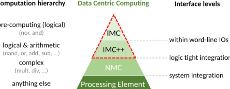
Several solutions have been studying the data-centric ar-chitecture. We classify these solutions from a complexity instruction point of view, as shown in Figure 1, according to the computation locality in the memory. Moreover, in our topology we do not consider emerging technologies, as Non Volatile Memory (NVM), which propose a different approach to IMC. NMC refers to any accelerator that is integrated near
pre-computing (logical)
(nor, and)
logical & arithmetic
(nand, or, add, sub, …)
complex
(mult, div, …)
Data Centric Computing
IMC IMC++ Processing Element NMC anything else Computation hierarchy
within word-line IOs logic tight integration system integration
Interface levels
Fig. 1 Data-centric computing solutions classification
the memory to reduce data movement between two or more memory instances. For the IMC, a part of the calculation is pre-computed inside the memory between two or more word-lines via the bit-lines. Then an Arithmetic Logic Unit (ALU) and a Finite State Machine (FSM) allow the support of boolean, logical and arithmetic operations at the bottom of the columns. In related work [4], [6], [9], IMC can only perform logical operations (AND, OR, XOR, NOT,...) or bit-serial logical and arithmetical operations [7]. In [5], the authors pushed further the IMC concept by adding a larger instruction set to support logical and arithmetic vector operations, in this paper we call it IMC++. All other complex operations are sent to be performed directly in the Central Processing Unit (CPU). We aim to maximize as many computations as possible at the IMC level in order to minimize data movements.
Security and cryptographic applications have been demon-strated in [10] and [4] with part of crypto-computation per-formed inside the memory bit-cell. Speed up can reach 6.8× in performances and 12.8× in energy saving versus state-of-the-art crypto benchmarks running on Cortex M0+ architecture. Other work [9] use machine learning applications able to perform classification directly inside SRAM memory. Thanks to Convolutional Neural Network (CNN) topology trained with MNIST image database, this low-power imager has 13× energy saving improvements compared to a standard training system.
Regarding IMC combined with NMC, we find different implementations of this solution like in [3], which exhibits data-centric applications (text processing, databases, check-pointing) explorations and [11] which explore neural networks, vision and graph processing. Replacing IMC and NMC inside a cache hierarchy, increase speed up by 1.9× and reduce energy by 2.4× compare to a conventional processor with 256-bit wide vector units.
To conclude, these papers focus on single IMC based architecture or larger system but without considering detailed memory interconnects. In this paper, we propose to explore multiple IMC tile-based architecture, proposing and using a detailed performance model of interconnected IMC tiles.
III. APPLICATION EXPLORATION FORIMC
In this section, we explore specific test cases requiring a majority of logical operations to perform them with IMC (bitwise only). Through the literature, we found security and cryptographic applications, pattern matching in a database [12]
or string searching in a text [3] and binary neural networks applications [13]. Those applications exploit logical operators that can be efficiently executed inside the memory array. A. Application exploration for IMC bitwise operations
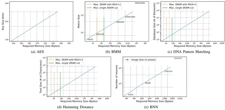
Advanced Encryption Standard (AES) [10] is a crypto-graphic applications use for security purposes. One encryp-tion consists by reading fixed input data blocks of 128-bits, choosing a key size of 128, 192 or 256 bits and performing computation steps to obtain an encrypted block of 128 bits. This cypher text can be decrypted by using the same key size. Computation steps are performed using AND, SHIFT and XOR operations.
Boolean Matrix Multiplication (BMM) [14] can be used in computer vision but also to find the shortest path in oriented graphs, discrete structures by associating an adjacency matrix to represent the graph or context-free grammar parsing. This algorithm uses mostly AND to replace multiplication and OR to replace addition operators to result a boolean sum.
DNA Pattern Matching [12] includes several algorithms that can use logical operators to improve performances of bio-informatic applications. Also called Exact Pattern Matching or String Searching algorithms, they all try to find a match of a pattern/string inside a database/text. Pattern and database are composed of a finite alphabet, which could be changed according to the applications.
Hamming Distance [12] is an algorithm used in coding theory and can return a value corresponding to the number of different symbols present between two strings having the same length. A derivation of this algorithm, called Hamming weight or Population count (popcount) is also famous in Binary Neural Networks and consists to return the number of symbols that are different from the zero-symbol (e.g. return the number of ones). Thanks to this features, we can sum binary values using bitwise operators.
Binary Neural Networks (BNN) [15] are today a new approach of Neural Network systems that replace n-bits by 1-bit data width (constrained to {-1/+1}) and most of the arithmetic operators by bitwise operators (e.g. XNOR and popcount). By reducing the number of weights, they also reduce the data movement, increase the throughput and save power and energy.
B. Application exploration in simulation
Applications Logical ops. Other ops.
logical ops. % of AES and, shift, xor add 66% BMM and, or add, cmp 50% DNA Pattern Matching and, not, or, shift add, sub 50% Hamming Distance and, shift, xor add, cmp, sub 66% BNN and, shift, xnor add, cmp, sub 95%
TABLE I: Applications instructions comparison We explore all those applications by unrolling the program execution. The idea is to quantify the number of logical operations used when the program is executed. We have developed a test environment based on the LLVM Compiler
160 180 200 220 240 260 280 300
Required Memory Size (Bytes)
128 192 256
Key Size (bits)
(a) AES
2k 8k 32k 128k 512k 2M 8M
Required Memory Size (Bytes)
102 103 Matrix Size 50x50 100x100 500x500 1000x1000 5000x5000
Max. SRAM with MUX=1 Max. single SRAM cut
(b) BMM
4k 16k 64k 256k 1M 4M 16M 64M 256M
Required Memory Size (Bytes)
104 105 106 107 108 109 Datab ase Size (# of Elements)
Max. SRAM with MUX=1 Max. single SRAM cut
(c) DNA Pattern Matching
4k 16k 64k 256k 1M 4M 16M 64M
Required Memory Size (Bytes)
103 104 105 106 107 108 Text Si ze ( # of Char acters)
Max. SRAM with MUX=1 Max. single SRAM cut
(d) Hamming Distance
4M 8M 16M 32M 64M 128M 256M 512M
Required Memory Size (Bytes)
105 106 Number of neurons 32x32 96x96 224x224 512x512
Image Size (in pixels)
(e) BNN Fig. 2 Memory sizing of five test case applications
Infrastructure [16]. We ensure that all applications are opti-mized and use the maximum number of boolean operations.
In Table I, we present logical operation’s dependencies for each application. All the applications are using arithmetic operation for comparing and incrementing the iterators within the loops of the algorithm. Except for the BNN application, all the other application include at least 50% of logical operation, which is the maximum speed up versus a single core architecture with a SRAM. Thus, the IMC is not sufficient to accelerate their computation without considering parallel improvement.
C. Memory requirements
In this study, we target applications with large data memory, which means that data cannot fit inside a single memory instance. A memory instance or memory cut is usually com-posed by an array of bit-cells, sense amplifiers, a column and row decoder and a control logic. Within the bit-cell array, columns can be interleaved and the multiplexer (MUX) can select a column which is related to a data’s address. In Figure 2, we plot two vertical lines corresponding to memory cut specifications defined by the STMicroelectronics memory cut explorer:
• vertical orange dotted line: indicates the maximum memory size available with a single row multiplexer (not interleaved). In literature, IMC requires this feature to perform computation of one vector in one cycle, because operands are stored on the same column line.
• vertical green solid line: indicates the maximum mem-ory size available. After this size, all designs must be a composition of different memory instances and we should consider the wire cost (see Section V).
To satisfy data memory requirements of each application, we size the memory according to their input parameters. Regarding these five applications presented in Figure 2, we can conclude that a single memory instance is, as expected, not enough to store those data memory sizes, except for AES application. To obtain a large memory, one can choose to design a single large memory instance or to design a multiple instances system with small instance interconnected to each other. For a single huge memory instance, performance will be limited by the power supply, RC and sense amplifiers. For that reason, we build a multiple memory systems using an interconnect wiring in order to access to data.
In the rest of our study, we develop a wire model to estimate this interconnect cost.
IV. TOWARDS ANIMC TILEBASEDARCHITECTURE
A. Proposed Architecture
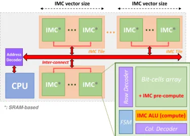
In this paper, we propose a scalable IMC tile-based architec-ture (Figure 3), inspired by classic Single Instruction Multiple Data (SIMD) architectures. IMC can be considered as vector computing because each bit-line performs 1-bit-computation between two or multiple word-lines. In that perspective, each operation is comprised of vectors operating in all SRAM memory instance which support IMC. Those data could be vectorized and aligned in order to size the data memory. To explore data centric architecture, we need to evaluate data movement of applications and develop an interconnect model to measure performance and energy trade-offs between them. Figure 3 represents a 2D scalable IMC cluster that is composed of multiple IMC tiles, themselves composed of multiple SRAM memory instances supporting IMC. In order to reduce dynamic power consumption, only the required IMC
Fig. 3 2D-Vector scalable IMC tile-based architecture
instance is selected by using the adequate low level signaling (memory chip select and clock gating). In this architecture, each IMC tile can have its own vector width in order to perform vector computations of different sizes in parallel. A host CPU can compute dedicated operation that IMC tile cannot perform and send IMC instructions for each IMC tile. Total memory of the cluster can be resized in width by the maximum vector size of the application and in height thanks to the total memory requirement. In terms of performance modeling and computation, we consider an IMC instance like a standard SRAM memory which is able to perform logical operations and having the same timing access. Thanks to this model, we are able to compare a IMC-based with a SRAM-based architectures.
B. Interconnect and Control challenges
In an IMC tile-based architecture, several assumptions must be taken into account:
• The memory storage must store the data aligned by vec-tors in order to perform the same word-line computation on multiple memory instances,
• All results must be stored in the same memory instance to avoid data movement between memory instances,
• There must be no data movement between memories in order to keep synchronization between memory intances. Vectorization and Parallelism - Thanks to the proposed IMC architecture [5], we can enable vectorization and par-allelism by running multiple instances in parallel. Here, the vectorization allows an acceleration proportional to the size of the vector used by IMC tile. Indeed, if the operation is executed in parallel, the size of the vector can theoretically be as large as desired. Unfortunately, by considering a realistic interconnect model, the wider the vector, the lower the per-formance will be. In other words, the vector size is the factor that will determine the performance of the system.
Apps Behavior(VHDL) Synthesis Place &Route Timings P.T. Power Model
Software & ExplorationPhysical Design Flow Analysis & Modeling
Parameters • Data width • # of cut(s) • Memory size P&R optimizations • 75% density • WNS: read data path
extractions inputs
Fig. 4 Physical design flow and modeling methodology
R ea d M ux SRAM SRAM SRAM SRAM D Q C E D Q A Read net delay Read logic delay Write net delay B D Write memory internal delay Read memory internal delay
Fig. 5 Write (A → C) and read (C → E) timing paths
(a) 2 cuts of 8kB (b) 16 cuts of 1kB (c) 64 cuts of 1kB Fig. 6 Floor plans of different designs - Legend: each pink object encircled by white is a memory instance, green nets represent wires on metal layer 4 (M4), yellow nets represent wire on metal layer 5 (M5) and blue nets represent wires on metal layer 6 (M6).
V. VALIDATION OF THE INTERCONNECT MODEL
To develop the interconnect model, we explore 22 different designs of SRAM tile-based architectures with various dimen-sional parameters and we extract results to create a model. We use 28nm FD-SOI SRAM memory instance database provid-ing a range of 10 custom sprovid-ingle memory instance optimized by STMicroelectronics (for a memory size of 64 Bytes up to 32 kB), interconnected to a 16-bit wide data bus. The IMC instances are interconnected using standard address/data protocol while adequate chip select per instance is done to reduce dynamic power consumption.
Between the actual SRAM and the proposed IMC tile-based design, the wiring cost will be the same (Figure 5: point D to point E), but we make the assumption of identical energy consumption.
A. Evaluation methodology
For each design of this study, we describe every architec-ture’s behaviours in VHDL then push them to RTL through
1 2 4 8 16 32 64 128 256 512 Memory Size (kB) 0.4 0.6 0.8 1.0 1.2 1.4 1.6 Read A ccess Time (n s) wiring cost (61%) wiring cost (43%) wiring cost (25%) wiring cost (10%) 1 cut + wiring 1 cut + no wiring 4 cuts + wiring 4 cuts + no wiring 16 cuts + wiring 16 cuts + no wiring 64 cuts + wiring 64 cuts + no wiring (a) 0.6 0.8 1.0 1.2 1.4 1.6 1.8 2.0 Performance (ns) 0 2 4 6 8 10 12 14 Energy (pJ) 1 2 4 8 16 32 64 1 2 4 8 16 32 64 128 1 2 4 8 16 32 64 128 2 4 8 16 32 64 128 8 16 32 64 128 16 32 64 128 32 64 128 78% 49% LOWER IS BETTER (on the x-axis and y-axis)
Total memory size 512 kB 256 kB 128 kB 64 kB 32 kB 16 kB 4 kB (b)
Fig. 7 Wiring costs, timings and power results. (a) Performance (read timings) versus memory size for various multi-cuts. Each curve has a given number of memory instances (cuts). (b) Energy (static and dynamic) versus performance for different memory sizes. Each dot label value represents the total number of memory instances (cuts).
a synthesis and a Place&Route flow, as shown in Figure 4. After timing extractions, we observe that the Worst Negative Slack (WNS) time is the path between reading a data from the memory to the register used in the CPU. Indeed, our critical reading path is composed of the memory internal delay, net delay and the logic delay, from point C to point E as shown in Figure 5. In every designs, we target the optimal symmetrical tiling, as shown in Figure 6, which has the lower slack time for the read path and ensure a design density of 75%. To measure our wiring cost, we consider the path between the point D to E which include wiring nets and the distribution logic. To create our model, we change the dimensional parameters for 22 designs as the number of instances, the memory size and the memory pattern shape. After place and route step, we extract the total area, timings and power results thanks to Innovus and PrimeTime Power Cadence softwares.
B. Experimental Results
Figure 7a puts into perspective the performance of multiple designs composed of 1, 4, 16 and 64 memory instances (cuts). Each curve uses a fixed number of memory instances for a given size. For example, to obtain the red curve for a memory size of 64kB, the architecture is composed of 16 memory cut of 4kB each. We observe that single cut will have much better performance if we need small memory sizes but have higher latency if we scale a larger memory size. Indeed, for 1kB memory size design has a performance gain of 7% when comparing 1-cut versus 4-cut curves but become 17% better for the 4-cut design at a memory size of 32 kB. In addition, the wiring cost is proportional to the number of instances used (10% of the performance for 1 cut and 25% of the performance for 4 instances) and this should be taken into consideration.
1 2 4 8 16 32 64 128 256 512 Number of cuts 0.0 2.5 5.0 7.5 10.0 12.5 15.0 17.5 Total Energy (pJ)
memory idle energy
single active memory cut energy memory leakage
all other gates (clock tree,...) area (right axis)
0.0 0.2 0.4 0.6 0.8 Ar ea (m m 2)
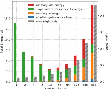
Fig. 8 Total energy and area for a sweep of the number of cuts composing a 32 kB memory. x-axis: number of cuts needed to obtain a memory size of a 32 kB.
Figure 7b shows the trade-offs between energy and perfor-mance between designs with varying memory sizes (equivalent to the number of memory instances). For example, the green curve represents all designs composed by single to multiple memory instances for a total memory size of 32kB. If we design an architecture requiring 32kB of data memory, we can find the best proposed design by using a 16 multi-cuts of 2kB. We can improve performance by 49% compare to a 128 multi-cuts design and 78% in energy compared to a single cut. As shown in Figure 8, there are energy trade-offs related to
the number of memory instance for a given memory size. We note that the wiring energy cost is negligible (represented in ”all other gates” section) in every designs because the power consumed by the memories is much bigger. Multiple memory instances designs have a higher static leakage than single instance. In every designs, only one single memory instance is accessed (Figure 8: ”single active memory cut energy” section) an the other memory instances are in idle energy mode (Figure 8: ”memory idle energy” section). To conclude, for a memory size of 32 kB, 16 cuts of 2 kB seem to be the multi-instances design with the lower energy trade-off and an acceptable area compared to 512-cut design.
C. Discussions
The study proposed in this paper allows to precisely size our scalable IMC architecture according to power, performances and area trade-offs. This wiring cost becomes limiting for the performance of our IMC cluster. Indeed, the more the required memory size increases, the more performance decreases. As we have seen in the Section IV-B there are specific conditions for the operation of the IMC. The idea is to use NMC as a processing engine close to the memory in order to solve the problems of moving data between memory instances in a multi-IMC architecture, but also dedicated to alignment to enable vector computations.
VI. CONCLUSION
Architectures implementing data centric computing improve throughput performance but change the architecture. In order to propose an optimized architecture for these data-intensive applications, a precise interconnect cost model is required. In this paper, we presented a methodology that allows the exploration and sizing of architecture through a model vali-dated in a 28nm FD-SOI technology. It is a useful tool for circuit designers who want to have an accurate estimation of the wiring cost in a scalable architecture. Applied to the problem of the memory wall, it shows the gains achieved through the use of IMC. Indeed, the more memory the application requires, the higher the wiring cost increases and the more the performance and power gains with IMC increase. IMC also brings performance gains through vectorization and parallelism proportional and equal to at most the number of memory instances used.
In our future works, we will push the wire cost model fur-ther and develop a wire cost model for 3D technologies using emerging technologies in order to find the ideal trade-offs between the requirements of the applications and a scalable IMC 3D tile-based architecture.
REFERENCES
[1] M. Horowitz, “1.1 computing’s energy problem (and what we can do about it),” in 2014 IEEE International Solid-State Circuits Conference Digest of Technical Papers (ISSCC). IEEE, 2014, pp. 10–14. [2] T. Agerwala and M. Perrone, “Data centric systems, the next paradigm
in computing,” 2014.
[3] S. Aga, S. Jeloka, A. Subramaniyan, S. Narayanasamy, D. Blaauw, and R. Das, “Compute caches,” in 2017 IEEE International Symposium on High Performance Computer Architecture (HPCA), 2017, pp. 481–492. [4] A. Agrawal, A. Jaiswal, C. Lee, and K. Roy, “X-SRAM: Enabling in-memory boolean computations in CMOS static random access memo-ries,” IEEE Transactions on Circuits and Systems I: Regular Papers, pp. 1–14, 2018.
[5] K. C. Akyel, H. P. Charles, J. Mottin, B. Giraud, G. Suraci, S. Thuries, and J. P. Noel, “DRC2: Dynamically reconfigurable computing circuit based on memory architecture,” in 2016 IEEE International Conference on Rebooting Computing (ICRC), 2016, pp. 1–8.
[6] Q. Dong, S. Jeloka, M. Saligane, Y. Kim, M. Kawaminami, A. Harada, S. Miyoshi, M. Yasuda, D. Blaauw, and D. Sylvester, “A 4 + 2t SRAM for searching and in-memory computing with 0.3-v VDDmin,” IEEE Journal of Solid-State Circuits, vol. 53, no. 99, pp. 1006–1015, 2017. [7] J. Wang, X. Wang, C. Eckert, A. Subramaniyan, R. Das, D. Blaauw,
and D. Sylvester, “A compute SRAM with bit-serial integer/floating-point operations for programmable in-memory vector acceleration,” in 2019 IEEE International Solid-State Circuits Conference (ISSCC), 2019, pp. 224–226.
[8] G. Singh, L. Chelini, S. Corda, A. J. Awan, S. Stuijk, R. Jordans, H. Corporaal, and A. Boonstra, “A review of near-memory computing architectures: Opportunities and challenges,” in 2018 21st Euromicro Conference on Digital System Design (DSD), 2018, pp. 608–617. [9] J. Zhang, Z. Wang, and N. Verma, “In-memory computation of a
machine-learning classifier in a standard 6t SRAM array,” IEEE Journal of Solid-State Circuits, vol. 52, no. 4, pp. 915–924, 2017.
[10] Y. Zhang, L. Xu, Q. Dong, J. Wang, D. Blaauw, and D. Sylvester, “Recryptor: A reconfigurable cryptographic cortex-m0 processor with in-memory and near-memory computing for IoT security,” IEEE Journal of Solid-State Circuits, vol. 53, no. 99, pp. 995–1005, 2018.
[11] F. Schuiki, M. Schaffner, F. K. Grkaynak, and L. Benini, “A scalable near-memory architecture for training deep neural networks on large in-memory datasets,” IEEE Transactions on Computers, vol. 68, no. 4, pp. 484–497, 2019.
[12] S. Faro and T. Lecroq, “The exact online string matching problem: a review of the most recent results,” ACM Computing Surveys (CSUR), vol. 45, no. 2, 2013.
[13] C. Eckert, X. Wang, J. Wang, A. Subramaniyan, R. Iyer, D. Sylvester, D. Blaaauw, and R. Das, “Neural cache: Bit-serial in-cache acceleration of deep neural networks,” in 2018 ACM/IEEE 45th Annual International Symposium on Computer Architecture (ISCA), 2018, pp. 383–396. [14] H. Yu, “An improved combinatorial algorithm for boolean matrix
multiplication,” Information and Computation, vol. 261, pp. 240 – 247. [15] X. Lin, C. Zhao, and W. Pan, “Towards accurate binary convolutional neural network,” in Advances in Neural Information Processing Systems 30. Curran Associates, Inc., 2017, pp. 345–353.
[16] M. Kooli, H. Charles, C. Touzet, B. Giraud, and J. Nol, “Software platform dedicated for in-memory computing circuit evaluation,” in 2017 International Symposium on Rapid System Prototyping (RSP), 2017, pp. 43–49.