HAL Id: hal-01827056
https://hal.archives-ouvertes.fr/hal-01827056
Submitted on 1 Jul 2018
HAL is a multi-disciplinary open access
archive for the deposit and dissemination of
sci-entific research documents, whether they are
pub-lished or not. The documents may come from
teaching and research institutions in France or
abroad, or from public or private research centers.
L’archive ouverte pluridisciplinaire HAL, est
destinée au dépôt et à la diffusion de documents
scientifiques de niveau recherche, publiés ou non,
émanant des établissements d’enseignement et de
recherche français ou étrangers, des laboratoires
publics ou privés.
Learning with memristive devices: How should we
model their behavior?
Damien Querlioz, Philippe Dollfus, Olivier Bichler, Christian Gamrat
To cite this version:
Damien Querlioz, Philippe Dollfus, Olivier Bichler, Christian Gamrat.
Learning with
mem-ristive devices:
How should we model their behavior?.
2011 IEEE/ACM International
Sym-posium on Nanoscale Architectures (NANOARCH), Jun 2011, San Diego, United States.
�10.1109/NANOARCH.2011.5941497�. �hal-01827056�
Learning with memristive devices: how should we
model their behavior?
Damien Querlioz, Philippe Dollfus
Institut d’Electronique FondamentaleUniv. Paris-Sud ,CNRS Orsay, France [email protected]
Olivier Bichler, Christian Gamrat
CEA, LISTEmbedded Computers Laboratory Gif-Sur-Yvette, France
Abstract—This work discusses the modeling of memristive
devices, for architectures where they are used as synapses. It is shown that the most common models used in this context do not always accurately reflect the actual behavior of popular devices in pulse regime. We introduce a new behavioral model, intended towards the nanoarchitecture community. It fits the conductance evolution of Univ. Michigan’s synaptic memristive devices. A variation of the model fits HP labs’s memristors’ behavior in the same conditions. Finally, we discuss using a simple example the importance of this type of modeling for learning architectures and how it can impact the behavior of the learning.
Keywords-component; formatting; style; styling; insert (key words)
I. INTRODUCTION
In recent years, memristive devices have emerged as a fantastic opportunity for renewal in electronic systems. Memristive devices are a family of two-terminal devices whose resistance evolves according to the bias and currents they experience [1]. Different applications fields have been targeted for such technology. Memory and reprogrammable logic are probably the most direct application of memristive devices and other nanoscale switches [2]-[9]. A reinvention of logic using schemes appropriate to their device physics has also been proposed [10]. Most current proposals, however, do not exploit the multivalued resistance capability (analog memory) which is a fantastic property of some memristive technology. HP lab’s original memristors [1] have this feature. It is present in Univ. Michigan’s synaptic devices [11], and others [12],[13]. It has also been reported in memristive three-terminal devices (optically gated carbon nanotube FETs [14],[15], nanoparticle organic memory FETs [16], Palermo organic devices [17] and UCLA ionic transistors [18]).
A currently highly researched approach is to use such memristive devices as synapses for learning [19], since this may be a way to exploit the intermediate resistance states of the devices, with relaxed requirements on the controllability of such states. Various proposals go into that direction. Some use conventional artificial neural networks [20],[21], a concept that has been experimentally demonstrated in [15]. Some use novel approaches inspired directly by Biology (like amoeba learning [22]). Finally, a popular idea is to associate memristive devices with spiking neural networks (neural networks that compute with asynchronous spikes, like the brain). It has indeed been
suggested [23],[24],[25] and shown experimentally [11] that memristive devices can implement a learning rule observed in biological synapses (Spike Timing Dependent Plasticity [26]). In different contexts, this rule has been shown to have important potential for machine learning [27],[28].
Such research could lead to particularly innovative electronic architectures and develop intelligent and low power electronic systems able to learn and to adapt themselves to their environment. Many explorations are now performed in this direction, both on devices and architectures. A serious difficulty for the “nanoarchitects” working in that field, however, is that the many memristive technologies that exist rely on different physics. Therefore, they can have extremely different behaviors, which can lead to different results if used for learning. To invent the applications of memristive technology, we have to rely on simplified models of devices. Are they sufficient? How do they compare with the actual technology developed in device labs, especially in “learning-type” situations?
In this paper, we review the most popular device models used to develop nano-architectures capable of learning with memristive devices and introduce a new one. We then compare these models with measurements from two popular technologies for use as synapses that rely on different physics: Univ. Michigan’s nanoscale synapses [11] and HP Labs’s TiO2 memristors [1]. We explore strengths and weaknesses of the models and conclude how we believe memristive devices should be considered for studies involving learning.
II. MEMRISTOR MODELS FOR LEARNING
A. The original linear memristor model (model A)
Different models have been used by nanoarchitects for exploratory studies that aim at taking advantage of multivalued resistance capability of memristive devices. Actually, memristors were introduced by HP Labs using a simple model [1] taking inspiration from Chua’s pioneering views on the “fourth passive element”, the memristor [29]. In HP’s model, a memristor of thickness D has two layers: one of low linear resistance RON, and the second (of thickness w) of high
resistance ROFF. The device resistance is therefore:
RRON
Dw
ROFFw This work was supported by the European Union through the FP7 Project NABAB (Contract FP7-216777).
The front between the two regions evolves according to (where µ is the front mobility)
i
D R dt
dw ON
which leads to:
R V i dt dR
(where we have introduced
ROFF RON
RON D). The resistance is additionally bounded between a minimum and a maximum value ( Rmin DRON and Rmax DROFF respectively).Using the devices for learning usually involves repeated, short voltage pulses that aim at changing the conductance of the devices only moderately [20]-[23]. Some learning proposals also involved more complex voltage pulses [24], but understanding the effect of constant voltage pulses is an important step in order to grasp how learning could be done with memristive devices. In addition, we focus primarily on conductance because it corresponds to the synaptic weights in the context of neural networks and thus has more significance than resistance for learning. If the voltage V during such a pulse is constant, the conductance of the device evolves as
3 3 VG R V dt dG
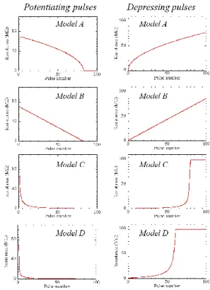
This law leads to small conductance steps when conductance is low, and to large conductance steps when conductance is already high. The two top plots of Fig. 1 illustrate how this behaves in situation (the model parameters are listed in Table 1). On the left graph we apply a series of short “potentiating” (i.e. V<0 with the convention used within this paper) identical pulses and plot the conductance of the device after each pulse. The conductance increase starts slowly and accelerates sharply after 70 pulses until conductance reaches the maximum conductance of the device. On the right graph we apply a series of “depressing” (i.e. V>0) pulses. In this case, the conductance decrease starts rapidly and then slows down after 10 pulses. In both cases, the envelope of the curve conductance vs. N is in 1/N2 (where N is the number of pulses). In this paper, these two series of repeated pulses are the reference experiments to identify how memristive devices behave in a learning situation.
If we plot the device resistance instead of its conductance (top plots of Fig. 2), the same qualitative behavior is seen, but is not as sharp, the resistance steps being in 1/R. The envelope of the curve is in log N.
Figure 1. Conductance vs pulse number for a serie of “potentiating” (V=-1V) voltage pulses (left) and depressive (V=+1V) pulses (right) with the four devices models (pulse durations: 1 ms). From top to bottom: linear memristor (model A), threshold models (models B and C), asymmetric model (model D).
Model parameters are listed in Table I.
B. Threshold model (models B and C)
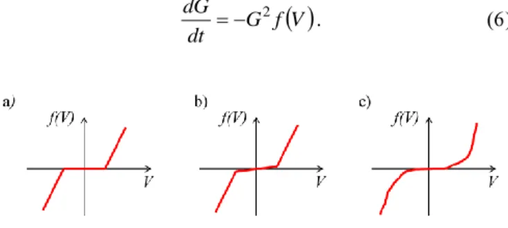
Though particularly helpful to understand how memristive devices work, the linear memristor model lacks important properties of actual devices. In this model, the time derivative of resistance is proportional to the current. This is not the case for actual devices that are all deeply nonlinear. Most devices even have a threshold voltage below which they experience no or little change [10],[11]. This makes a huge difference for nanoarchitectures since this allows probing the resistance state without changing it, and should be accounted for when designing them. Therefore, other models have been developed that include a threshold effect. We introduce the most commonly used model, for example by Snider [30], Pershin [22] or Linares-Barranco [24] (model B). The device resistance evolves as:
f
Vdt
dR
where f is generally nonlinear, typically a hyperbolic or piecewise linear function, as illustrated on Fig. 3. This leads to (for a constant voltage pulse)
G f
Vdt
dG 2
Figure 3. Examples of typically used f functions for equations (5) to (11), to model the nonlinearity of resistance change depending on the voltage applied
across the device.
On the second line of Fig. 1 and 2, we illustrate the behavior of this model in the same test situation used for the linear memristor model. Conductance evolution (Fig. 1) is actually similar: potentiation (left graph) starts slow and accelerates, and depression (right graph) starts rapidly and decelerates. The envelope of the curve is 1/N instead of 1/N² in the linear memristor case. The resistance (Fig. 2) has, however, a distinct and characteristic feature: it is a linear function of pulse number. This should be recognizable immediately on measured devices if they behave consistently with this model.
A variation (model C) is also used by nanoarchitects [21]. It consists of the same model, with conductance instead of resistance: f
V dt dG which leads to R f
V dt dR 2 As illustrated on the third line of Figs. 1 and 2, the behavior is identical to model B, but with conductance and resistance inverted. On experimental devices, this behavior should be easily recognizable by the linear behavior of the conductance with pulse number.
C. Asymmetric model (model D)
We finally introduce a new model that we will show to have value in matching with device measurements. Unlike all the other models, the conductance change is asymmetric for potentiation and depression. For negative voltages (leading to increase of the conductance, or potentiation), we model the change of conductance with:
max min min G G G G e V f dt dG The more potentiated it is, the smaller the step. For positive voltages (depression), the expression is similar:
max min max G G G G e V f dt dG For the resistance, this translates to
dt dG R dt dR 2
The behavior of this model is illustrated on the last lines of Figs. 1 and 2. The conductance (Fig. 1) curves are different from that of the other models. Depression (left graph) starts rapidly and then slows down (in models A and B it starts slowly and accelerates, in model C it is linear). Potentiation also starts rapidly and then slows down (which is similar to models A and B). This asymmetry of potentiation and depression should be easy to recognize in experiments.
Resistance behavior (Fig. 2) is different due to the competition between R² and exponential in the resistance derivative, and may look different depending on the parameters of the model.
III. CONFRONTATION WITH CURRENT TECHNOLOGY
Figure 4. Schematization of the two kind of devices considered . a) Univ Michigan nanoscale synapses. The position of the front between Ag-rich and
Ag-poor regions determines conductance, b) HP Labs’ TiO2 memristors.Conductance is determined by the thickness of a barrier at the
A. Univ. Michigan’s nanoscale synapses
We first study devices from [11]. They are a variation of the devices introduced in previous works [31],[32], but specifically targeted toward synaptic operation with continuous variation of the resistance (whereas the original devices had binary resistance, i.e. distinct low and high resistance states). The physics of these devices actually seems close to the original memristor model. Silver is cosputtered with the device thin film material (silicon), on top of a silver-free layer of thin film. An electric field moves the silver atoms giving rise to Ag-rich and Ag-poor regions, the width of which defining the device conductance (Fig. 4, a). Thus, unlike many resistive memory technologies and the group’s previous samples, these devices do not switch by rupturing or reforming filaments (in which case a more binary switching behavior is obtained).
Fig. 5 plots (red diamonds) measurements on these devices reproduced from [11]. On the left plot, devices were subjected to brief -3.2 V potentiating pulses, and the conductance after each pulse (measured by 1 V read pulses) is plotted. On the right plot the same is done with depressing (2.8 V) pulses. Fig. 6 plots the corresponding resistance data. As seen on Fig 5 conductance can indeed be tuned finely by the short voltage pulses. However, neither the conductance nor the resistance is linear in respect to pulse number. This invalidates both models B and C for this technology. We also notice an extremely asymmetric behavior between potentiation and depression. They both start rapidly and then slow down. This invalidates model A. By contrast model D can fit the measurements (blue line in Fig. 1 and Fig. 2) and thus seems appropriate for architectural studies. More experimental data will be needed however to fit f+(V) and f-(V) for other voltages than those
reported in [11].
Figure 5. Evolution of the conductance for the devices from Michigan, fitted with the model D. Left: device conductance (measured at 1 V) after each pulse
in a serie of potentiating (V=-3.2V) pulses. Right: same with depressing (V=2.8V) pulses. Diamond: experimental data, reproduced from [11]. Full
line: Model D (parameters listed in Table I).
Figure 6. Same as Fig. 5 with resistance.
B. HP TiO2 memristors
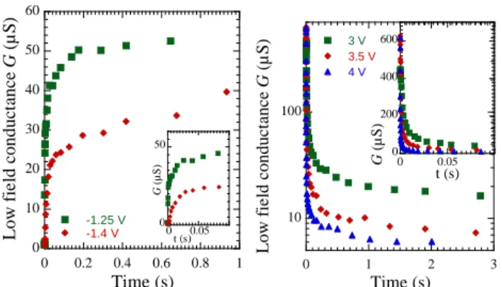
Figure 7. Tunneling gap width w as a function of time in a serie of potentitation (left) or depressing (right) pulses on HP memristors (symbols: experimental data from [33], full line: Model D), for different pulse voltages (left: -1.4 and -1.25 V; right: 4, 3.5 and 3 V). Insets show details of the figure
for short times. Model D parameters are listed in Table I.
Figure 8. Low field conductance computed from tunneling gap width w from Fig 7 in the same conditions. For depressing pulse, conductance is shown in a log scale because of its abrupt change. The insets (details for short time) are
both in linear scale.
HP Labs’ TiO2 memristors were first introduced with a simple physical interpretation [1]. The physical view has largely progressed with subsequent experiments and analysis [34],[35],[36]. Comprehensive characteristics of their dynamical behavior at room temperature were introduced in [33] and are used as a reference in this paper. The devices appear to operate via modulation of tunnel barrier width at the end of a conductive channel that was obtained by 0 20 40 0 20 40 60 80 100 Co ndu cta nce ( nS) Pulse number 0 20 40 0 20 40 60 80 100 Co ndu cta nce ( nS) Pulse number 0 200 400 0 20 40 60 80 100 Resi stan c e (M ) Pulse number 0 200 400 0 20 40 60 80 100 Resi stan c e (M ) Pulse number 1.4 1.6 1.8 0 0.2 0.4 0.6 0.8 1 -1.25 V -1.4 V T un ne l gap wid th (nm) Time (s) 1.6 0 0.05 w ( n m ) t (s) 1 1.2 1.4 1.6 1.8 0 0.5 1 1.5 2 2.5 3 3 V 3.5 V 4 V Tu nnel gap wi dth (nm ) Time (s) 1.2 1.6 0 0.05 w ( nm) t (s) 0 10 20 30 40 50 60 0 0.2 0.4 0.6 0.8 1 -1.25 V -1.4 V Lo w fi e ld co ndu ct ance G (µ S ) Time (s) 0 50 0 0.05 G (µ S ) t (s) 10 100 0 1 2 3 3 V 3.5 V 4 V Time (s) Lo w f ie ld co ndu ct ance G (µ S ) 0 200 400 600 0 0.05 t (s) G ( µS )
electroformation (Fig. 4, b) [33]. The tunnel width w is the essential state parameter that can be connected to current by the model presented in [37] and in the supplementary information of [33].
In [33], the authors extracted the parameter w as a function of time t after potentiating and depressing voltage pulses. This is plotted on Fig. 7 (left: potentiating, right: depressing). This data was obtained by repeating voltage pulses whose duration was not constant. That is why the graphs are plotted as a function of time and not pulse number, and can still be read similarly to the previous plots of this paper. On Fig. 8, we converted w into a low field conductance using the well-established model given in [33]. Potentiation (left) starts with an extremely abrupt increase of conductance and then becomes a lot slower. Similarly depression (right) starts with an extremely abrupt decrease of conductance, and then becomes a lot slower. Among our models, only model D has this behavior. The initial increase or decrease of conductance is however so abrupt that Fig. 8 cannot be fitted by model D. Without any change, none of our device model is thus appropriate.
Interestingly, however, the evolution of w can be fitted roughly by the equations of model D, with w taking the place of conductance G (full lines of Fig. 7). The fit is not perfect, but can give an acceptable model of device behavior for architectural studies. Alternatively the full model given in [33] may be used, but is a lot more complex than model D.
The reason for which these devices (unlike Michigan’s) cannot be fitted by model D directly seems to be due to the tunneling aspect of transport. If the conductance had a linear dependence on w, model D would work, but the conductance is rather an exponential function of w. This extremely abrupt start of the potentiation and depression would have significant impact if the device is used for learning.
IV. DISCUSSION
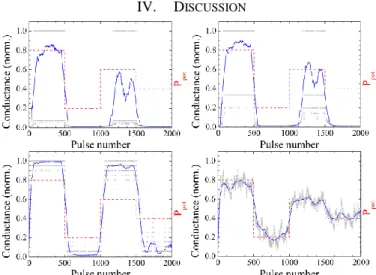
Figure 9. Conductance as a function of the potentiating / depressing pulses ratio for the four models described above. From top-left to bottom-right: linear
memristor (model A, top, left), threshold models (models B, top, right, and C,bottom, left) and asymmetric model (model D, bottom, right). The dashed red curve is the probability Ppot of the pulse to be a potentiating pulse and the
blue curve is a moving average of the conductance of the device.
We have seen in part II that the different models used for designing learning architectures with memristive devices lead to qualitatively different conductance evolution dynamics when voltage pulses are used to change the conductance (these pulses constituting a baseline at evaluating memristive device modeling for learning architectures). In that regard, a significant difference between the common models (A, B, C) and the new model D is that models A, B, C use symmetric equations for potentiating (V<0) and depressing (V>0) pulses, whereas model D uses asymmetric equations. In particular, for models A and B, this implies that if a device is in low conductance state, potentiating pulses (pulses that increase the conductance) have a small effect and a number of them is required before potentiation becomes efficient. Whereas with model D, for a device with a low conductance, the first potentiating pulses cause the most conductance change, and then potentiation slows down (assuming identical pulses). In part III, we have seen how two popular devices actually behave more like the new model D. Michigan’s devices can be fitted by model D. In HP’s devices, the state’s variable w may be roughly modeled by model D, and the conductance switches abruptly when the device is in a low or high conductance state.
Now, how important is it to catch this behavior correctly when developing nanoarchitectures capable of learning? It seems to be significantly, in that the considered memristive device behavior can have significant repercussions on the learning strategy that needs to be put in place. To illustrate this point, we performed a simple computational experiment. We simulated the behavior of the four models for a series of 2000 pulses of either potentiating type (with a probability of Ppot) or
depressing type (with a probability of 1 - Ppot). In Fig. 9, we
show the evolution of the conductance for each model for different values of the probability Ppot (0.8, 0.2, 0.6, and 0.4
successively). It is noteworthy that the mean conductance approximates the probability Ppot for the asymmetric model
(model D). For the models A and B, the initial increase in conductivity being very slow compared to its initial decrease, the mean conductance stay close to zero for low values of the probability Ppot. The model C has a different behavior: since
the conductivity change is independent of the current state of the device, the conductivity always tends to increase when Ppot
> 0.5 and decrease when Ppot < 0.5 .The conductance of the
device therefore does not stabilize to intermediate values with this simple scheme.
This illustrates that the type of learning will be different depending on the model used. In model A and B, low conductance states are extremely stable. In model C, the memristive device is naturally led to low or high conductance states that are more stable. In model D, depending on the model parameters, any intermediate resistance can be stable. Of course, the simple computational experiment presented above does not preclude the learning of stable arbitrary conductance states with devices best modeled by models A, B or C. It suggests, however, that the commonly used models that may look similar will give very different results regarding the final state of learning.
V. CONCLUSION
In this work, we first saw that the equations (linear memristor A, and threshold models B and C) commonly used to model the conductance change of memristive device in nanoarchitectures lead to significantly different behaviors when used with short voltage pulses. Such pulses are fundamental for nanoarchitectures involving learning. We then presented two memristive technologies targeted towards learning, and saw that their behavior matched none of these common models. For both devices, potentiation (the process that increases the conductance of the memristors) and depression (the processes that decreases it) are extremely asymmetric, which none of the three models captures. The new model that we introduced (asymmetric model D) corrects this issue and fits measurements on Univ. Michigan’s synaptic devices directly, and after an adaptation measurements on HP Labs’ original memristors. Finally, we pointed with a simple simulation that using one or the other of the models will change the stability of the memristors’ states in a learning situation. All this suggests that existing memristors’ models should be used with caution when developing this kind of architectures.
TABLE I. MODEL PARAMETERS USED IN THIS PAPER
Figure Model parameters
Fig. 1, 2 model A 1.25.10 12²/V/ms Fig. 1, 2 model B f(1V)=-f(-1V)=0.85 M/ms Fig. 1, 2 model C f(1V)=-f(-1V)=12.5 nS/ms Fig. 1, 2 model D = 2.0, = 3.5, f+(1V)= 40 nS/ms, f- (-1V)=150 nS/ms Fig. 1,2
all models Gmin = 10 nS, Gmax = 1 µS
Fig. 5,6 = 3.0, = 2.8, f+(1V)= 600 nS/ms, f- (-1V)=900 nS/ms, Gmin = 3.3 nS, Gmax = 40 nS Fig. 7 Potentation: = 20.0, f+ (-1.4V)= 0.1 mm/s, f+ (-1.25V)= 0.9 mm/s, wmin=1.3nm, wmax=1.8 nm Depression: (4 V, 3.5 V, 3 V) = 14.2, 13.0, 14.8, f(4 V, 3.5 V, 3 V) = 0.0026, 0.0028, 0.23 mm/s, wmin=1.1nm, wmax=1.65nm ACKNOWLEDGMENTS
We would like to thank D. Chabi, J.-O. Klein, W. Zhao, J. Saint-Martin and V. Derycke.
REFERENCES
[1] D.B. Strukov, G.S. Snider, D.R. Stewart, and R.S. Williams, “The missing memristor found,” Nature, vol. 453, May. 2008, pp. 80-83.
[2] D.B. Strukov and K.K. Likharev, “CMOL FPGA: a reconfigurable architecture for hybrid digital circuits with two-terminal nanodevices,”
Nanotechnology, vol. 16, 2005, pp. 888-900.
[3] J.R. Heath, P.J. Kuekes, G.S. Snider, and R.S. Williams, “A defect-tolerant computer architecture: Opportunities for nanotechnology,”
Science, vol. 280, 1998, p. 1716--1721.
[4] A. DeHon, “Array-based architecture for FET-based, nanoscale electronics,” IEEE Trans. Nanotechnol., vol. 2, 2003, pp. 23-32.
[5] A. DeHon and K.K. Likharev, “Hybrid CMOS/nanoelectronic digital circuits: devices, architectures, and design automation,” Proceedings of
the 2005 IEEE/ACM Int. conf. on Computer-aided design, Washington, DC,
USA: IEEE Computer Society, 2005, p. 375–382.
[6] D.B. Strukov and R.S. Williams, “Four-dimensional address topology for circuits with stacked multilayer crossbar arrays,” PNAS, vol. 106, Dec. 2009, pp. 20155 -20158.
[7] J. Borghetti, Z. Li, J. Straznicky, X. Li, D.A.A. Ohlberg, W. Wu, D.R. Stewart, and R.S. Williams, “A hybrid nanomemristor/transistor logic circuit capable of selfprogramming,” PNAS, vol. 106, Feb. 2009, pp. 1699 -1703.
[8] E. Linn, R. Rosezin, C. Kugeler, and R. Waser, “Complementary resistive switches for passive nanocrossbar memories,” Nat. Mater., vol. 9, May. 2010, pp. 403-406.
[9] Q. Xia, W. Robinett, M.W. Cumbie, N. Banerjee, T.J. Cardinali, J.J. Yang, W. Wu, X. Li, W.M. Tong, D.B. Strukov, G.S. Snider, G. Medeiros-Ribeiro, and R.S. Williams, “Memristor−CMOS Hybrid Integrated Circuits for Reconfigurable Logic,” Nano Lett., vol. 9, Oct. 2009, pp. 3640-3645.
[10] J. Borghetti, G.S. Snider, P.J. Kuekes, J.J. Yang, D.R. Stewart, and R.S. Williams, “`Memristive’ switches enable `stateful’ logic operations via material implication,” Nature, vol. 464, Apr. 2010, pp. 873-876.
[11] S.H. Jo, T. Chang, I. Ebong, B.B. Bhadviya, P. Mazumder, and W. Lu, “Nanoscale Memristor Device as Synapse in Neuromorphic Systems,”
Nano Lett., vol. 10, Apr. 2010, pp. 1297-1301.
[12] H. Choi, H. Jung, J. Lee, J. Yoon, J. Park, D.-jun Seong, W. Lee, M. Hasan, G.-Y. Jung, and H. Hwang, “An electrically modifiable synapse array of resistive switching memory,” Nanotechnol., vol. 20, 2009, p. 345201. [13] S. Yu, Y. Wu, and H.-S.P. Wong, “Investigating the switching dynamics and multilevel capability of bipolar metal oxide resistive switching memory,” Appl. Phys. Lett., vol. 98, 2011, p. 103514.
[14] W.S. Zhao, G. Agnus, V. Derycke, A. Filoramo, J.-P. Bourgoin, and C. Gamrat, “Nanotube devices based crossbar architecture: toward neuromorphic computing,” Nanotechnol., vol. 21, 2010, p. 175202.
[15] S.-Y. Liao, J.-M. Retrouvey, G. Agnus, W. Zhao, C. Maneux, S. Fregonese, T. Zimmer, D. Chabi, A. Filoramo, V. Derycke, C. Gamrat, and J.-O. Klein, “Design and Modeling of a Neuro-Inspired Learning Circuit Using Nanotube-Based Memory Devices,” IEEE Trans. Circuits Syst. Regul. Pap., in press.
[16] F. Alibart, S. Pleutin, D. Guérin, C. Novembre, S. Lenfant, K. Lmimouni, C. Gamrat, and D. Vuillaume, “An Organic Nanoparticle Transistor Behaving as a Biological Spiking Synapse,” Adv. Funct. Mater., vol. 20, 2010, pp. 330-337.
[17] V. Erokhin, T. Berzina, and M.P. Fontana, “Hybrid electronic device based on polyaniline-polyethyleneoxide junction,” J. Appl. Phys., vol. 97, 2005, p. 064501.
[18] Q. Lai, L. Zhang, Z. Li, W.F. Stickle, R.S. Williams, and Y. Chen, “Ionic/Electronic Hybrid Materials Integrated in a Synaptic Transistor with Signal Processing and Learning Functions,” Adv. Mater., vol. 22, 2010, pp. 2448-2453.
[19] M. Versace and B. Chandler, “The brain of a new machine,” IEEE
Spectrum, vol. 47, 2010, pp. 30-37.
[20] J.H. Lee and K.K. Likharev, “Defect-tolerant nanoelectronic pattern classifiers,” Int. J. Circuit Theory Appl., vol. 35, 2007, pp. 239-264. [21] D. Chabi and J.-O. Klein, “Hight fault tolerance in neural crossbar,” Int. Conf. on Design and Technology of Integrated Systems in
Nanoscale Era (DTIS), 2010, pp. 1-6.
[22] Y.V. Pershin, S. La Fontaine, and M. Di Ventra, “Memristive model of amoeba learning,” Physical Review E, vol. 80, 2009, p. 021926. [23] G.S. Snider, “Spike-timing-dependent learning in memristive nanodevices,” Prof. of IEEE International Symposium on Nanoscale
Architectures 2008 (NANOARCH), 2008, pp. 85-92.
[24] J.A. P rez-Carrasco, C. Zamarreño-Ramos, T. Serrano-Gotarredona, and B. Linares-Barranco, “On neuromorphic spiking architectures for asynchronous STDP memristive systems,” Proc. of 2010
IEEE Int. Symp. on Circuits and Systems (ISCAS), 2010, pp. 1659-1662.
[25] D. Querlioz, O. Bichler, and C. Gamrat, “A memristor-based spiking neural network immune to device variations,” Proc. of IJCNN 2011, in press.
[26] H. Markram, J. Lubke, M. Frotscher, and B. Sakmann, “Regulation of Synaptic Efficacy by Coincidence of Postsynaptic APs and EPSPs,” Science, vol. 275, Jan. 1997, pp. 213-215.
[27] T. Masquelier and S.J. Thorpe, “Unsupervised Learning of Visual Features through Spike Timing Dependent Plasticity,” PLoS Comput Biol, vol. 3, Feb. 2007, p. e31.
[28] B. Nessler, M. Pfeiffer, and W. Maass, “STDP enables spiking neurons to detect hidden causes of their inputs,” Advances in Neural
Information Processing Systems (NIPS’09), p. 1357–1365.
Transactions on Circuit Theory, vol. 18, 1971, pp. 507-519.
[30] G.S. Snider, “Self-organized computation with unreliable, memristive nanodevices,” Nanotechnol., vol. 18, 2007, p. 365202.
[31] S.H. Jo, K.-H. Kim, and W. Lu, “Programmable Resistance Switching in Nanoscale Two-Terminal Devices,” Nano Lett., vol. 9, Jan. 2009, pp. 496-500.
[32] S.H. Jo and W. Lu, “CMOS Compatible Nanoscale Nonvolatile Resistance Switching Memory,” Nano Lett., vol. 8, Feb. 2008, pp. 392-397. [33] M.D. Pickett, D.B. Strukov, J.L. Borghetti, J.J. Yang, G.S. Snider, D.R. Stewart, and R.S. Williams, “Switching dynamics in titanium dioxide memristive devices,” J. Appl. Phys., vol. 106, 2009, p. 074508.
[34] D.B. Strukov, J.L. Borghetti, and R.S. Williams, “Coupled Ionic and Electronic Transport Model of Thin-Film Semiconductor Memristive
Behavior,” Small, vol. 5, 2009, pp. 1058-1063.
[35] D.B. Strukov and R.S. Williams, “Exponential ionic drift: fast switching and low volatility of thin-film memristors,” Appl. Phys. A, vol. 94, 2008, pp. 515-519.
[36] J. Borghetti, D.B. Strukov, M.D. Pickett, J.J. Yang, D.R. Stewart, and R.S. Williams, “Electrical transport and thermometry of electroformed titanium dioxide memristive switches,” J. Appl. Phys., vol. 106, 2009,p. 124504.
[37] J.G. Simmons, “Generalized Formula for the Electric Tunnel Effect between Similar Electrodes Separated by a Thin Insulating Film,” J.