Correlation of Silicon Microroughness With Electrical
Parameters of SOI-AS (Silicon-On-Insulator With
Active Substrate)
by
Hasan M. Nayfeh
Submitted to the Department of Electrical Engineering
and Computer Science in partial fulfillment of the
requirements for the degree of M.S.
at the
MASSACHUSETTS INSTITUTE OF TECHNOLOGY
May
22,
1998
© Hasan M. Nayfeh, MCMXCVIII. All rights reserved.
The author hereby grants to MIT permission to reproduce
and distribute publicly paper and electronic copies of this
thesis document in whole or in part, and to grant others
the right to do so.
Author .
., ...Department of Electrical Engineering and Computer Science
May 22, 1998
Certified by ,
... ...Dimitri A. Antoniadis
ssor of Electrical Engineering
,
,
Tesis Sypervisor
Accepted by ...
- - -r -. • . .. , •o .o o . .... ... ...Artur C. Smith
Professor of Electrical Engineering
Graduate Officer
Correlation of Silicon Microroughness on Electrical Parameters of
SOIAS (Silicon-On-Insulator With Active Substrate)
by
Hasan M. Nayfeh
Submitted to the Department of Electrical Engineering and
Com-puter Science on May 22, 1998, in partial fulfillment of the
requirements for the degree of
Master of Science in Electrical Engineering and Computer Science
Abstract
The technology of the formation of SOIAS (Silicon-on-Insulator With Active Substrate) requires us to utilize the lower quality back side surface of the silicon film of the original Separation by Implantation of Oxygen (SIMOX) wafer. Transistor action occurs within a distance of approximately ten nanometers from the top silicon surface. This calls for an investigation and optimization of the surface properties of SOIAS. Novel chemical
mechanical polishing (CMP) techniques were used to achieve surface roughness values as good as bulk silicon (2-3 Angstroms). Electrical parameters were determined by measur-ing the interface state density (Dit) usmeasur-ing charge pumpmeasur-ing, and the dielectric breakdown using time-zero breakdown (TZBD). The effective mobility (PEff) has been measured as a function of vertical electric field. Surface characterization was performed using atomic force microscopy (AFM). The relationship between surface roughness and these parame-ters has been determined by measuring the above electrical parameparame-ters on fabricated gated P-i-N diodes and NMOS transistors with different surface roughness.
This work has discovered that the electrical performance of SOIAS is slightly improved by polishing.The mobility has been shown to be capable of matching or exceeding bulk-Si devices. A SOIAS wafer with a 8% smaller roughness than its bulk counterpart has a 9% larger surface mobility at an effective electric field of 0.8 MV/cm. The trend of improving mobility is also found amongst SOIAS wafers themselves as it is found that a 97% reduc-tion in surface roughness leads to a 16% increase in mobility. Moreover, comparing two SOIAS wafers, the roughest and the smoothest, we discover that reducing the roughness by a factor of 92% reduces the interface trap density by 22%. However, the interface trap density could not be reduced to values measured on bulk-Si for SOIAS wafers polished to comparable roughness. However, it was found that polished samples have less on-wafer variation of Dit. This is a requirement for the microelectronics industry since that then translates into threshold voltage control on chip. It has also been found that oxide reliabil-ity does not depend upon the surface roughness.
Thesis Supervisor: Dimitri A. Antoniadis
Acknowledgments
Many people helped in making this thesis possible. I would first like to thank my advisor Profes-sor Dimitri Antoniadis for supporting me and giving me the opportunity to pursue this research in his group. I am also grateful to my colleagues in the group. I would like to thank Tony Lochtefeld whose help was crucial in performing this work. He was my mentor for my first year here, teach-ing me all the essentials of research in SOIAS. He continued to be helpful throughout my project. I would also like to thank my officemates Zachary Lee and Ilia Sokolinski. I also would like to thank Mark Armstrong, Melanie Sherony, Andy Wei, and Keith Jackson for all their help. I would also like to thank the staff of MTL whose help was essential. Vicky Diadiuk, Patricia Burkhart, Bernard Alamariu, Tom Takacs, Paul Tierney, Dan Adams, Ron Stoute, Joe Walsh, Kurt Broderick. All of you thanks so much.
I would like to thank all my friends for all the fun times playing sports, going out, and sharing jokes.
I would also like to thank Elizabeth Shaw at the Center for Material Science and Engineering (CMSE) for training me and allowing me to use their AFM.
Thanks to Professor Hank Smith for allowing me to use the AFM at the NSL, and Euclid Moon for training me on it.
I acknowledge Jim Shen from Rodel for providing me with the recipe for polishing the samples. I acknowledge IBIS Corp. for providing me with SIMOX wafers.
I would like to acknowledge the DoD (Department of Defense) for funding me with a fellowship during the course of this research. I would also like to acknowedge DARPA for supporting part of this work.
Finally, I would like to thank my family for all their support: Munir and Hutaf Nayfeh, parents
Maha Nayfeh, sister Ammar Nayfeh, brother Osama Nayfeh, brother Mona Nayfeh, sister
Table of Contents
1 Introduction 11
1.1 M otivation ... . ... 11
1.2 Previous Work in Correlating Surface Roughness with Electrical Parametersl2 1.3 G oal of T hesis ... 13
2 Background on Semiconductor Surface Science 15 2.1 Importance of Surface in Device Performance ... 15
2.2 The Si/SiO2 Interface ... ... ... ... 16
3 Background on SOIAS 19 3.1 Introduction to SOIAS ... 19
3.2 Previous Work Done in SOIAS ... ... 19
4 Building SOIAS Wafers 21 4 .1 W hy S O IA S ? ... 2 1 4.2 Different Methods of Creating SOIAS Wafers... ... 22
4.3 SOIAS Wafer Preparation... ... 24
5 Wafer Characterization 27 5.1 Determination of Silicon film thickness using Ellipsometry Techniques ... 27
5.2 Determination of Silicon Morphology Using AFM...29
5.3 Discussion of AFM Results ... 51
6 Improving Morphology 55 6.1 Chemical Mechanical Polishing (CMP) ... ... 55
6.2 H ow C M P W orks ... 55
6.3 CMP Experiments at MIT... 57
7 Measurements 59 7.1 Fabricated D evices ... 59
7.2 Device Characterization ... 59
7.3 Interface State Density (Dit) ... 60
7.4 Charge Pumping Experimental Setup/Measurement ... ... 62
7.5 Actual Determination of Dit ... 64
7.6 Time-Zero Dielectric Breakdown (TZDB) ... 66
7.7 T Z D B R esults ... ... 68
7.8 Effective M obility (m eff)... 72
7.9 Analysis of Results ... .. .. ... 75
8 Conclusion 81 8.1 F inal R em arks ... 8 1 8.2 Future W ork ... .... ... ... 82
B ibliograp hy ... ... 83
Appendix A MTL NMOS Process Flow For Material Characterization Devices ... 87
A. 1 PROCESS TRAVELER-MSOIAS 1 ... ... 87
A.2 Processing and Fabrication ... 92
Facility 92 Touch Polish & AFM Imaging of Morphology 93 Thinning of Film Thickness 93 Defining Active Regions 94 Lithography 94 Etch for final active region definition 95 Formation of Field Area 96 Gate Definition 97 Channel Implant 97 Source Drain Regions 102 Final Steps 103 A.3 Supreme Program Calculation of Dose and Energy of Vt Implant ... 105
A.4 TMAH Etch For Silicon Substrate Removal ... 109
A .5 A FM O peration ... ... ... 110
A .6 C M P R ecipe ... ... 111
A ppendix B ... ... ... 115
Appendix B Electrical M easurem ents... ... 115
B. IV Curves ... 115
List of Figures
SOIAS W afer ... ... ... 25
Steps for creation of SOIAS wafer... ... 26
Schematic of AFM [31]... 30
Piezoresistive Cantilever Detection Set-Up ... ... 31
Piezo Tube Scanner Used in AFM ... ... 32
Dimension 3000 SPM With Motorized X-Y Stage ... 40
AFM Image SOIAS2... 41
AFM Image SOIAS3... 41
AFM Image SOIAS4... 41
AFM Image SOIAS5... 42
AFM Image SOIAS6... 42
Figure 5.10: AFM Image SOIAS7 ... ... 43
Figure 5.11: Figure 5.12: Figure 5.13: Figure 5.14: Figure 5.15: Figure 5.16: Figure 5.17: Figure 5.18: Figure 5.19: Figure 5.20: Figure 5.21: AFM AFM AFM AFM AFM AFM AFM AFM AFM AFM AFM Image Image Image Image Image Image Image Image Image Image Image SO IA S 8 ... ... 43 SO IA S9 ... ... 44 S O IA S 10 ... 44
SIMOX Wafer SOI6S ... 45
SOIAS 2- touch polished ... 45
SOIAS 3 -touch polished ... .... 46
SOIAS 4- touch polished ... 46
SOIAS 6- touch polished ... .... 46
SOIAS 7- touch polished ... .... 47
SOIAS 10- touch polished ... 47
of Bulk Wafer ... 47
Figure 5.22: AFM Image Touch Polished SIMOX Wafer (SOI3S) ... 48
Figure 5.23: Percentage Change of Morphology Parameters With Polish Time...50
Figure 5.24: Wafer 8C after polishing ... 53
Figure 5.25: Wafer 8C after oxidation thinning... ... ... 53
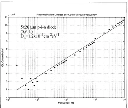
Figure 7.1: B ulk2 Signature ... 63
Figure 7.2: Bulk2 Dit Determination ... 64
Figure 7.3: Dit Versus Interface Roughness- Several Samples ... 65
Figure 7.4: Dit Versus Roughness ... ... ... 66
Figure 7.5: TZDB CURVES ... ... ... 69
Figure 7.6: Fowler Nordheim SOIAS2, 3, 6, 7... ... 70
Figure 7.7: Fowler Nordheim SOIAS8,10, SOI3S,6S ... 70
Figure 7.8: Fowler Nordheim Bulk2... 71
Figure 7.9: Roughness Versus Efield @ IG=lpA ... ... 72
Figure 7.10: Effective Mobility Versus Effective Electric Field...74
Figure 7.11: Surface Mobility Versus Surface Roughness For Eeff=0.8 MV/cm...75
Figure 2.1: B U L K IV ... ... ... ... 115
Figure 2.2: BULK Vt calculation... ... 116
Figure 2.3: BULK2 SS Calculation ... 116 Figure 4.1: Figure 4.2: Figure 5.1: Figure 5.2: Figure 5.3: Figure 5.4: Figure 5.5: Figure 5.6: Figure 5.7: Figure 5.8: Figure 5.9:
Figure 2.4: IV SOI3S ... 117
Figure 2.5: SOI3S Vt Calculation... 117
Figure 2.6: SOI3S SS Calculation ... 118
Figure 2.7: SO I6S IV Calculation... 18
Figure 2.8: SOI6S Vt Calculation... 119
Figure 2.9: SOI6S SS Calculation ... 19
Figure 2.10: IV SO IA S 10 ... 120
Figure 2.11: SOIAS10 Vt Calculation ... 120
Figure 2.12: SOIAS10 SS Calculation ... 121
Figure 2.13: IV SOIAS2 ... 121
Figure 2.14: Vt Calculation SOIAS2 ... 122
Figure 2.15: SOIAS2 SS Calculation ... 122
Figure 2.16: SOIAS3 IV Curves ... 123
Figure 2.17: SOIAS3 Vt Calculation ... 123
Figure 2.18: SOIA S3 SS Calculation ... ... 124
Figure 2.19: SOIAS6 IV Curves ... 124
Figure 2.20: SOIAS6 Vt Calculation ... 125
Figure 2.21: SOIA S6 SS Calculation ... 125
Figure 2.22: SOIAS7 IV Curves ... 126
Figure 2.23: SOIAS7 SS Calculation ... 127
Figure 2.24: SOIA S8 IV Curves ... ... 127
Figure 2.25: SOIA S8 Vt Calculation ... 128
Figure 2.26: SOIAS8 SS Calculation ... ... 128
Figure 2.1: SOIAS2 Signature ... 129
Figure 2.2: SOIAS3 Signature ... .. 129
Figure 2.3: SOIAS7 Signature ... 130
Figure 2.4: SOIAS8 Signature ... ... 130
Figure 2.5: SO I3S Signature ... ... 131
Figure 2.6: SO I6S Signature ... 131
Figure 2.7: SOIAS2 Dit Determination ... 132
Figure 2.8: SOIAS3 Dit Determination ... 132
Figure 2.9: SOIAS7 Dit Determination ... 133
Figure 2.10: SOIAS8 Dit Determination ... 133
Figure 2.11: SOIAS 10 Dit Determination ... 134
Figure 2.12: SOI3S Dit Determination ... 134
List of Tables
Table 3.1: Average Interface Trap Density For Different Substrate Materials [10] 20 Table 5.1: SOIAS WAFERS BEFORE TOUCH POLISH 48
Table 5.2: SOIAS WAFERS and SOI WAFERS AFTER TOUCH POLISH 49 Table 5.3: Percent Change of Morphology Parameters (+/- Increase/Reduction) 49
Table 5.4: Piranha, Pirahna+HF Effect on Morphology 50 Table 6.1: Touch Polish of SIMOX Dummies 57
Table 6.2: Touch-Polish Experiment Results on SOIAS Wafers 58 Table 6.3: Touch Polish SOI Wafers 58
Table 7.1: Dit Numbers 65 Table 1.1: SOIAS Wafers 87 Table 1.2: SOI Wafers 87 Table 1.1: SF6 Nitride Etch 95
Table 1.2: Oxidation Furnace Schedule 100 Table 1.3: CC14 Poly Si etch 101
Chapter 1
Introduction
The SOIAS (Silicon on Insulator with Active Substrate) process previously developed at MIT allows the transfer of a thin single-crystalline layer of device-quality silicon from a
SOI wafer to a bulk carry-wafer allowing 3D integration.
This project investigates the relationship between the surface morphology of the sili-con film of this novel SOI-based technology and its electrical parameters. The SOIAS involves integration in the third dimension, allowing the formation of a buried gate and possibly other interconnect layers. This gate can be used as a back-gate control of the threshold voltage of devices. This leads to large savings in power consumption, and conse-quently can be used for ultra-low-power application. A proper study of the silicon film quality of SOIAS must be conducted in order for this technology to emerge as a force in the semiconductor industry.
1.1 Motivation
The theory of why surface roughness affects electrical properties is that atomic roughness is the physical origin of surface states [1]. This gives impurities sites to reside in at the sur-face and hence results in higher values for intersur-face state density Dit. These sites can then be occupied by carriers causing lower values of mobility. Furthermore, if the trapped car-rier has an electric charge, the mobility will also be degraded due to coulombic scattering. In addition, as the scaling down of transistor dimensions becomes a viable thrust for the industry to achieve larger density of integrated circuits, reduction of the oxide thickness becomes mandatory. This poses a serious challenge to avoid dielectric breakdown. The
quality of the Si-Si0 2 will be crucial in achieving this goal. Hahn et al. [4] reports that
bumps at the irregular Si-SiO2 interface. Therefore, a surface with atomic smoothness
must be produced using chemical mechanical polishing (CMP) in order to achieve high breakdown fields. Lin et al. report that there is a better coupling between gate voltage and surface potential due to smoother surfaces[15]; hence, a smoother surface is expected to
have higher mobilities. These above reasons, demonstrate that effects of Si/SiO2 interface
roughness are no longer negligible in device behavior for ULSI technology[23].
1.2 Previous Work in Correlating Surface Roughness with Electrical
Parameters
Determination of the relationship between the surface morphology of the silicon interface of transistors with electrical performance has been conducted for bulk silicon technology. Hahn et al. reports a strong correlation between Hall mobility and interface state density
with atomic roughness at the Si-Si0 2 interface at high inversion [1]. They show that a
larger surface roughness translates into a larger density of surface states and a lower value for mobility [1]. It has also been demonstrated that there is an increased interface state density Dit with an increase in surface roughness [20]. It is also shown that an increase in surface roughness reduces the field needed to breakdown the gate oxide.
Lin et al. performed a detailed study of the effects of surface roughness on the electri-cal properties of bulk Si devices. He found that interface roughness will:
1. Modulate the local surface electric field 2. Reduce the channel mobility
3. Enhance the Fowler-Nordheim Tunneling Current 4. Modify the quantum oscillation pattern
5. Diminish the hot carrier population 6. Slightly degrade the oxide strength
Chan et al. performed an experiment on thin film poly transistors to determine the con-tribution of surface morphology on the performance of devices. He did this by comparing devices that had polishing done on them to ones that had not. His experiments constantly showed that devices that were polished had the best performance. For example, there was a two-fold improvement of the drain current in saturation. In fact, wafers that were pol-ished gave higher field-effect mobility, higher saturation current, higher dielectric break-down strength, improved turn-on characteristics, and improved short channel behavior[ 15].
1.3 Goal of Thesis
This thesis attempts to determine the relationship between the surface morphology and electrical parameters of this novel SOI based structure. Several steps were taken in order to accomplish this goal. First, the wafers were prepared. This involved fabrication steps utilizing new and advanced technologies such as bonding. Secondly, a means of creating splits of different morphology was accomplished. This was done by touch-polishing wafers using CMP technology. Wafers then had their morphology improved dramatically using this and at the same time, the film thickness was a controlled parameter. Next, the wafer morphology was characterized by using state-of-the-art Atomic Force Microscopy to obtain and analyze pictures of the surface on an atomic scale. After that, a full process was done whereby special structures were fabricated that were used to study the electrical properties of the material. The structures were measured and the data was then correlated with the morphology data.
Chapter 2
Background on Semiconductor Surface Science
2.1 Importance of Surface in Device Performance
The surface of silicon plays a very important role in the performance of electron devices. The surface unlike the bulk of the material is an abrupt end so that the periodicity of the crystal is lost. This results in atoms at the surface having dangling bonds, hence, making it susceptible to contamination and giving rise to interface states which could be charged. In addition to this charge, there are charge centers located in the oxide which is grown on the silicon surface. The major cause of these centers are defects that are related to the
chemi-cal structure of the interface [25]. There are three types of charges in a Si/SiO2 structure
[25]:
1. Fixed Oxide Charge: The source of this charge is from structural defects in the oxide layer such as ionized silicon located in the oxide layer (-25 Angstroms from the Si/
SiO2 interface). Oxide fixed charge is defined as localized charge centers that cannot
change their charge state by exchange of mobile carriers with the silicon.
2. Mobile Oxide Charge: This is charge due to ionic impurities such as Na', Li+, K+
and possibly H+ .
3. Oxide trapped charge: This is from holes or electrons trapped in the bulk of the oxide. Possible source of this charge are ionizing radiation and avalanche injection.
4. Si/SiO2 Interface Trapped Charge: These are positive or negative charges. There
are three causes for it: (1) Structural, oxidation-induced defects, (2) metal impurities, or (3) defects caused by bond breaking processes such as radiation. Interface trap charges are charges localized on centers that can exchange charge state with the silicon. These charges
will change the electrostatics of the device and hence, they must be understood and mized in order to optimize device performance. One of the goals of this work is to mini-mize the fourth kind of charge- interface trapped charge by improving the morphology of
the Si/SiO2 interface using CMP.
2.2
The Si/SiO
2Interface
This quality of this interface is a prime indicator of the performance of a transistor device.
There are five features of the Si-SiO2 interface [25]:
1. The Si-SiO2 interface has charge centers called oxide fixed charge. The charges
have a positive polarity. They are immobile under an applied electric field. They do not exchange charge with the silicon when the gate bias is varied.
2. The interface has traps. The traps change occupancy with gate bias. They have energy levels distributed throughout the bandgap. They do not communicate with each other, so they do not form an energy band.
3. The interface potential varies at the interface from point to point due to random dis-tribution of localized charged interface traps and of the oxide fixed charge.
4. Individual interface trap capture cross sections may be distributed over a range of values due to bent or stretched bonds.
5. Interface trap characteristics of thermal oxidation are donor type in the upper half of
the bandgap.
As stated before, it has been demonstrated that a better quality interface in terms of morphology results in a smaller interface trap density Dit. Interface traps are within 10
angstroms of the Si-SiO2 interface, so it is not surprising that the morphology of the
possi-ble and then determine the relationship between the morphology and the quality of the interface.
Interface traps can be produced in several different ways [25]: 1. Thermal oxidation in dry oxygen or steam
2. Plasma Oxidation
3. Avalanche injection of electrons or holes into the SiO2
4. Diffusion of metals such as chromium to the Si-SiO2 interface
5. Exposure of the MOS system to ionizing radiation
There exist different models that explain the origin of interface traps [25]:
1. Coulombic Model: Claims that charges in the oxide induce potential wells in the silicon. The energy eigenvalues of these wells are the interface trap levels. The levels are located near the silicon band edges.
2. Bond Model: Claims that interface trap level distribution is produced by a distribu-tion of bond angles or by stretched bonds at the silicon surface. These could be due to
local strain or local nonstoichiometry at the Si-SiO2 interface.
3. Defect Model: Says that defects within or near the interfacial region cause interface trap levels. The defects could be stacking faults, micropores, or even various atomic or molecular fragments left as a residue of imperfect oxidation. Four types of defects: 1) excess silicon (trivalent silicon), 2) excess oxygen (nonbridging oxygen), 3) impurities, 4) states in the oxygen charge induced-potential wells. There are three sources of excess oxy-gen: 1) Due to the oxidation reaction, 2) the strain in the region might be relieved by for-mation of the excess oxygen defect, 3) there are water-related electron traps near the
Some of these defects can be removed by passivating the surface by hydrogen and as a result satisfying the valence bonds. However, interface traps due to surface morphology can not be annealed out. The morphology itself has to be improved in order to improve this factor. Another method of quantifying the quality of the interface is to determine the field for oxide breakdown. It has been shown that a bumpy surface will have enhanced fields, causing breakdown at a smaller voltage than a smoother surface. This field can be determined by performing a time zero dielectric breakdown measurement [10].
Chapter 3
Background on SOIAS
3.1 Introduction to SOIAS
The SOIAS (Silicon on Insulator on Active Substrate) is an improvement upon regular SOI technology [10]. The improvement is that a back-gate is implemented. This offers many advantages. The advantages are due to the fact that the back gate can control the threshold voltage of the device. This allows one to control the threshold voltage dynami-cally. For instance, when a system is in a standby mode, it dissipates power. To counter this, we can use the back-gate to increase the threshold voltage, so that this power is reduced; hence, SOIAS is a step towards achieving ultra-low power devices. Not only can we achieve low-power, but also we can achieve high performance by lowering the thresh-old voltage when we require high transconductance giving a higher current drive. In addi-tion, this back-gate scheme allows one to control the threshold voltage of a discrete device independently giving full control over every device on the chip.
3.2 Previous Work Done in SOIAS
Yang [10] has implemented a CMOS process on SOIAS substrates. Device and simple cir-cuit fabrication was successful. Yang achieved about three decades of switch in off current and a 1.5 times increase in drive current for both NMOS and PMOS at VDS of 1 Volt. Independent control of the back gates was also verified. It was shown that a 36% change in speed can be attained with 250 mV switch in threshold voltage at 1 V supply voltage. Also, large dynamic threshold voltage control was demonstrated. It was also shown that threshold voltage control is not deteriorated for effective channel length scaling down to -0.2 microns [10].
However, the Dit value for the bonded SIMOX SOIAS wafer (BSIMOX) was worse than its bulk and SOI counterparts. Here is a table giving the Dit values for 4 different sub-strates:
Average Interface States
Substrate Type -2e 1 (cm-ZeV') Bulk 3.1x10¹⁰ SOIAS (BESOI) 3.9x100 SIMOX 4.8x10 10 SOIAS (BSIMOX) 1.2x10¹¹
Table 3.1: Average Interface Trap Density For Different Substrate Materials [10] In this project, I will fabricate the BSIMOX SOIAS structure. As will be explained in Chapter 4, there are two methods of creating SOIAS wafers. Both start by using a SOI wafer, but SOI wafers can be created in several ways. Two popular methods are SIMOX (Separation by Implantation of Oxide) and BESOI (Bonded etch-backed SOI). It is known that the silicon quality is worse for SIMOX because of implantation damage to the crystal. The table acknowledges this. In this project, I created SOIAS wafers using SIMOX wafers. As can be seen from the table, the interface trap density is one order of magnitude large than bulk wafers, so there is plenty of room for optimization. A time zero dielectric breakdown measurement was also done for all four wafers. It demonstrated that the cumu-lative failure rate was almost the same for all types of wafers. The effective mobility of the four types of wafers was also calculated. That measurement showed that there is a slight improvement of mobility for smoother surfaces.
Chapter 4
Building SOIAS Wafers
4.1 Why SOIAS?
The goal of the SOIAS wafer is to create a means of controlling the threshold voltage other than using a well bias. This is done by creating a back gate inside the wafer. Figure 4.1 shows how the resulting structure should appear. We have a polysilicon film inside act-ing as the back gate. In addition to this, we also want to reap the benefits of SOI, so we want the wafer to be sitting on an insulating layer, and not to be in contact with the sub-strate.
The advantages of SOI are well known and understood. Present day technology uti-lizes bulk silicon wafers for fabrication of ULSI circuitry. Well formation in SOI is much simplified compared to bulk since there are no substrate effects. Also, in bulk-Si, there exists a parasitic effect called latch-up. It involves turning on a parasitic BJT which is composed of the source, drain and substrate regions. In SOI since we are dielectrically iso-lated from the substrate, we do not have latch-up problems. Latch-up forces one to sepa-rate wells of adjacent devices by a relatively large distance. In SOI, since there is no latch-up, we can pack more transistors per unit area. Another advantage is that SOI is not as sen-sitive to small perturbations. It offers better immunity to single-event upsets compared to bulk silicon because there is a smaller active silicon volume for charge to be collected. This causes SOI to be a good candidate for use in high radiation environments lending itself for many military and aerospace applications. Not only that, but sensitive charge memory devices like 1 G-bit DRAM built on SOI substrates are more reliable than their bulk counterparts [24].
SOI devices achieve higher circuit speeds and dissipate less power compared to bulk silicon devices[24]. Higher speeds can be achieved since SOI devices have smaller para-sitic capacitance. Namely, the source/drain to substrate capacitance is reduced dramati-cally because of the buried oxide separating the two. This lowering of the capacitance then gives a higher speed of operation.
Bulk silicon MOSFET devices have another parasitic effect. The source to body poten-tial difference makes the threshold voltage larger causing reduction of the drive current. SOI devices on the other hand have a much smaller body effect since the body is floating because of the oxide isolation. The larger drive current in SOI lends itself to higher speed applications compared to bulk devices.
4.2 Different Methods of Creating SOIAS Wafers
There exist several different methods of creating a SOIAS wafer using standard SOI mate-rial. Each method has its own advantages and disadvantages. These issues could be related to the complexity of the process, or the end products quality or a combination of the two. The difference in the methods is the type of SOI wafer one starts with. Presently, there are three major types of SOI wafers that have been fabricated and been proven to work. They are: SIMOX, BESOI, and Smart Cut.
1. SIMOX [8]: Separation by IMplantation of OXide, is considered to be the most advanced and promising for high density CMOS circuits [8]. It involves performing an implantation of oxygen ions into a bulk silicon wafer, and then performing a high temper-ature anneal to recover the crystal quality of the silicon. The formation of the oxide occurs by the ions chemically reacting with the silicon to form oxide precipitates. Since the molar volume of oxide is 1/0.44 times larger than silicon, extra space needs to be created to accommodate the oxide. This is done by an emission of Si interstitial atoms. This requires
breaking Si-Si chemical bonds which have an energy of -5 eV. This energy can be pro-vided by the bombarding ions themselves. After being emitted, the Si interstitials then migrate and reconstruct the surface and at the same time, they impede any further oxygen ion bombardment, so a steady state is reached. SIMOX wafers have a silicon thickness variation on the order of angstroms since it depends upon chemical reactions inside the bulk. Moreover, a desired thin film thickness is easily attained by altering the dose and energy of the ion bombardment.
2. BESOI [8]: Bonded Etch-back Silicon On Insulator utilizes bonding technology. The steps involved are: mating two silicon wafers together at room temperature, annealing the bonded wafers above 8000 C in order to increase the bonding strength, and then one of the wafers is thinned down by polishing [8]. The major disadvantage of BESOI is that it is difficult to attain very thin silicon films and at the same time have them be uniform on a macroscopic scale. This is the case, since polishing is used as the technique to achieve the required silicon thickness. An advantage of BESOI over SIMOX is that since no implanta-tion is involved, the material quality of the silicon film in BESOI is potentially better than SIMOX.
3. SMART CUT [8]: This method involves bonding two wafers together and then mechanically separating the bonded SOI layer from the original starting silicon substrate. This is done by implanting hydrogen. The wafer deleminates at the point where the hydro-gen ions exist. This technique has been shown to have a better thickness uniformity than SIMOX. Also, it allows one to reuse the silicon after the break, so it saves on supplies. However, much more research needs to be performed before this technology is used in mass production. At present, this technology needs more work to make it a more reliable
one. In this thesis, the wafers used to make SOIAS wafers will be SIMOX wafers. The SIMOX wafers obtained where from IBIS Corporation.
4.3 SOIAS Wafer Preparation
The formation of the SOIAS structure begins by creating a handle wafer. It is simply a bulk silicon wafer with a thermal oxide grown on top. This thermal oxide will serve as the dielectric isolation from the substrate like the buried oxide in SIMOX. On a separate stack, a thermal oxide is grown on top of a SIMOX wafer. This oxide will serve as the back-gate of the transistor to be. An amorphous silicon film is then grown on top of this oxide. This will serve as the back-gate material to be. This stack is then flipped and bonded to the han-dle wafer. Therefore, the bonding interface is between the thermal oxide and the amor-phous silicon.
Now, the silicon film from the SIMOX wafer is removed via wet etch using tetrame-thyl aluminum hydroxide (TMAH) solution. The buried SIMOX oxide serves as an etch stop so that the film thickness variation of the resulting silicon film is comparable to the original SIMOX silicon film. The final step is to etch the buried oxide using a diluted (7:1)
H20: HF buffered oxide etch (BOE) solution. One concern, however, is the occurrence of
silicon islands called inclusions. They occur a distance of about 25 nm from the bottom
interface. They have the same crystal orientation as the substrate and they are about 30 nm thick and 30 to 200 nm long [8]. So, after removing the Si with the TMAH, we first per-form a BOE etch to expose these islands in TMAH which are now near the top since we have flipped the SIMOX wafer. After that, we etch away the islands using these numbers as an indicator for the time required.
Figure 4. 1below shows the resulting five film structure.
SiO2
80-140 nm
80-100 nm 250 nm
Figure 4.1: SOIAS Wafer
Figure 4.2 below summarizes the steps taken to achieve the SOIAS structure.
Amorphous
Silicon
Back-gate
Oxide
'Silicon
Flip and bond
to handle wafer
SIMOX Buried Oxide
Oxide
I
Handle
Wafer
Etch SIMOX wafer
and buried oxide
Bonded
.Interface
Oxide
Silicon
-
Back-gate
Oxide
AmorphoL
Silicon
Figure 4.2: Steps for creation of SOIAS wafer
;;;;;;;;
::: : :::::::::-:::::::-::::::::-:::::::::::;:
::::::i:-::::::;:
:::: :: :::::::::::::::::::::;::
:i:-:::;::::::I::::::::;::::::::::
:-::::::::::
:::::
::::
:;:::::i:::::::::::::::::::::::::i::::
:::: ::::
:i::::::::
: :: : ::::::::::::::::::
::::::::
::::::::
:::::::
::::::
::::::
::::::::;:::::::
i::
::i:::::::;::
:;:
-i::-il:::::-:----:--;::-::--::-*:-i : ----:_;-:-::i-::::-:-::--:_-::-;::: :i:_ :-::-:- : ::_: _-- :::-::_--:i---i: :i-i::-:--::-i:-_:-:-i-__::-i-- : --:::_:-_-- ::---: :;ii::i:::::i_::::;:-_::i :i::::::_:-:_: :-::-:: ::::ii::::i:-i--i_:~-;-_::::::i- ----_:: :--_--:::-:-:::----:i-:--_-::_:::--:---: :i : :: :;:::::::;:;::::::;::::;::;::::: :::::::::::::::::::
Chapter
5
Wafer Characterization
After creating the wafers, a full analysis of the wafer was performed that includes determi-nation of the silicon film thickness and morphology of the surface.
5.1 Determination of Silicon film thickness using Ellipsometry
Tech-niques
There are two different techniques to determine the film thickness, one is spectroscopic ellipsometry and the other is standard ellipsometry. Spectroscopic ellipsometry is used to measure structures with more than two underlying films. This is the case for the SOIAS wafers, which have 4 films to take into account. This is possible since it uses a wide spread of different frequencies. Standard ellipsometry on the other hand is used for two films at most and uses one wavelength, namely the He-Ne laser (633 nm).
5.1.1 Spectroscopic Ellipsometry
Spectrosopic ellipsometry is a non-destructive method of determining the film thicknesses of a multi-film structure [26]. It works by shining a laser beam of variable wavelengths from a range of 230 nm to 930 nm and recording the change of amplitude of the beam and the change of phase and polarization [26]. The real and imaginary parts of the index of refraction are determined as a function of the wavelength of the incident light. They are both determined simultaneously, so one does not have to use the Kramer-Kronig disper-sion integrals [26]. From these data, the thickness can be deduced within an accuracy of 1 nm [26]. This method not only can determine thickness but also it can give information about crystallinity, void fraction, interface roughness and the composition of mixed lay-ers[26].
There are issues to watch for when performing a spectrosopic ellipsometry measure-ment. Light is reflected at the planar interface between a film and an ambient phase. One
obvious criterion is that this ambient phase must transmit light [26]. For our case, the ambient phase is the native oxide which grows on silicon. So this film must be taken into consideration for accurate results. In addition, the optical properties at the surface differ from deeper in the bulk. So surface states are an important consideration. The following effects should be accounted for: a contaminant or oxide film and a stressed beilby layer- (a layer with a high density of dislocations due to mechanical forces involved in the prepara-tion of the sample) [26]. This layer is most probably present on the wafers for this project due to the CMP. Finally, surface roughness is also an important consideration. All of these effects should be considered as a potential source of error.
5.1.2 Ellipsometry
Ellipsometry, on the other hand, works by shining a single frequency of light with ellipti-cal polarization from a He-Ne laser. From the fresnel equations, we can determine the reflectivity for the directions perpendicular and parallel to the plane of incidence respec-tively. These two reflectvities are different. In ellipsometry, we adjust the polarization of the incident beam such that the reflected beam is linearly polarized. From this, we can obtain two equations with the two unknowns being the complex index of refraction of the material, and the thickness of the material.
The ellipsometer can then, therefore, measure the following parameters [27]: * The complex index of refraction N=n+j 8
* The thickness of the film
From examination of the reflected linearly polarized beam, we can determine the relectivity of the parallel and perpendicular. We then can take the ratio of these two:
Rp/Rs = (Rpl/Rs)ei(APAs) = tan(T)eJA (5.1)
done by a computer program that can find the values.
Standard ellipsometry is a valuable technique for determining the optical properties of materials at wavelength regions where the materials are strong absorbing. It is also very
useful for small samples because it requires reflection from a small area (lmm2 or less)
[27]. One disadvantage of standard ellipsometry is that the measurement is dependent upon intensity fluctuations of the light source, since only the phase shifts are measured [8]. Spectroscopic ellipsometry was used to determine the film thicknesses of the SOIAS wafers and standard ellipsometry was used on the SOI wafers in conjunction with a spe-cial two-film program.
5.2
Determination of Silicon Morphology Using AFM
5.2.1 Introduction to AFM
Because interfaces have important implications for processing and device performances, AFM has been used to investigate both the (100) Si surface morphology and topogra-phy[16]. Before the invention of the AFM, light scattering or interferometric methods were used to determine roughness with an accuracy of sub-nanometer, but only in the ver-tical direction. Lateral resolution was on the scale of microns. The AFM has a resolution on the order of angstroms both in the lateral and vertical directions. AFM always one to laterally map a surface with a precision on the nanometer scale. Atomic resolution has been reported. It has been an instrumental tool in examining surfaces in modern technol-ogy.
Figure 5.1 below is a schematic of an AFM.
....-.
...
Detector
'
Cantilever
AFM tip
Forces
Sample surface
Piezo elements
Figure 5.1: Schematic of AFM [31]
As can be seen in Figure 5.1, the AFM consists of a sharp tip at the end of a soft canti-lever. As the tip is scanned across the sample, the cantilever bends under the effect of the particular tip-sample interaction being used by the probe. The AFM we use has a mono-lithic silicon tip and cantilever, with the tip having a radius of curvature of approximately 50nm. The small size of the cantilever (approximately 100pm x 50gam x lgm) permits it to have a low force constant, giving greater sensitivity and a high resonant frequency reduc-ing the effects of vibrations. Typically, the force constant of the cantilever is 1-50 N/m, while its resonant frequency is 100-400 kHz[31].
The cantilever deflection can be measured by two methods, optically and electrically. The electrical method monitors the resistance change in a piezoresistor built into the canti-lever. This method is useful when imaging light-sensitive samples. The AFM I used at
MIT uses an optical deflection-measurement system. Figure 5.2 shows a schematic of a deflection system based on the piezoresistor method.
WVheatstone bridge Figure 5.2: Piezoresistive Cantilever Detection Set-Up
The scanning element of the AFM consists of two parts. The sample rests on a stage with a helical underbody, supported by three piezoelectric tubes. This permits both the coarse approach of the sample to the tip, by rotating the stage with the piezotubes, and lat-eral motion of up to sevlat-eral millimeters in both directions. Fine positional control comes from the piezoelectric scan tube mounted vertically above the sample, to which the canti-lever is attached[31 ]. The AFM I used at MIT uses a motor for the coarse movements.
Fig-ure 5.3 shows the piezo tube used in our AFM here at MIT. It allows three dimensional
-Y
Figure 5.3: Piezo Tube Scanner Used in AFM
5.2.2 How the AFM Works
The principle of operation is based on a scientific phenomena called Van der Waals (VDW) forces. Two electrically neutral and non-magnetic bodies held at a distance of one to several tens of nanometers experience Van der Waals (VDW) forces [28]. VDW forces can be classified into 3 different categories- orientation, induction and dispersion [28]:
1. Orientation: this results from interaction between two polar molecules having per-manent multipole moments.
2. Induction: This is due to the interaction of a polar and a neutral molecule where the polar molecule induces polarity in the neutral molecule.
3. Dispersion: This is due to non-polar molecules having a small finite dipole which fluctuates causing an attractive force between the two molecules.
Dispersion is the most dominant of the three except for the special case when the two molecules are strong polar molecules. The VDW forces increase rapidly as the distance between the two molecules approach each other with a power law:
-7
F = s (5.2)
where s is the distance. If s is larger than several nanometers, the VDW forces become less effective as the:
-8
F = s (5.3)
As the AFM probe tip is brought closer to the sample, it is attracted by the long range VDW forces. Once the probe is very close to the surface, the electron orbitals of the atoms on the surface of the probe and sample start to repel each other. As the gap decreases, the repulsive forces dominate over the attractive forces. The forces depend on the distance from probe to sample, the probe geometry, and contamination on the sample surface. A force as small as 10 nN can be sensed. A map of the surface is obtained by maintaining a constant force and recording the deflection of the cantilever.
5.2.3 AFM Criteria
The criteria for an AFM is [28]: 1. vibration isolation
2. positioning devices 3. scanning units
4. electronic feedback system 5. computer automation
The force sensor has several criteria [28]:
1. The force constant has to small enough to allow detection of small forces. The force constant is determined by the material used to construct the cantilever as well as the
geom-etry.
2. The resonance frequency should be large in order to be insensitive to mechanical vibration since the mechanical vibration coupling is reduced by its frequency divided by the resonant frequency of the spring squared. Also, a high resonance frequency allows one to scan at a higher speed [28]. Typical resonance frequencies vary from 15kHz-500kHz. The resonant frequency is given by:
k
(0 = - (5.4)
m
where k is the elastic constant, and m is the mass. Since k is small, we then want the mass to be very small. The other constraint is the tip. The radius of the tip should be made as small as possible so that one can probe a small area of the sample.
3. To achieve atomic resolution, sharp tips with small effective radius of curvature are mandatory.
4. The angle the tip opens up should be as small as possible so one can probe into pits and troughs.
The mass of the tip should be made to be as small as possible. Tips are made by micro-machining materials such as silicon oxide, silicon nitride, and even bulk silicon. Before micromachining, each tip would have to be fabricated individually, for example, from dia-mond. Now, mass production of tips that are almost identical is possible due to microma-chining.
As an example, a typical microfabricated tip has a size of about 100 microns and a thickness of 1 micron. This gives a spring constant ranging from 0.1-1 N/m corresponding to a resonance frequency range of 10-100 kHz.
Tips with radius as small as 300 angstroms have been fabricated using micromachin-ing techniques. This is considerably larger than the size of an atom, but it can be used to image atoms since there exists protuding nanotips from this large radius.
An important issue is the detection of cantilever movement. The requirements for this are [28]:
1. High sensitivity at the sub-angstrom level
2. Independence of detection mechanism with cantilever movement.
There are several options of detection. One of these utilizes the phenomena of tunnel-ing. This is done by placing an STM tip opposite to the tip. The tunneling current from AFM tip to STM tip is then exponentially dependent upon the distance between them. This allows one to measure a deflection as small as 0.01 angstroms. The disadvantage of this method is that tunneling is dependent upon the surface quality of the cantilever. Also, the tunneling actually changes the spring constant of the cantilever. In addition, this method is not safe against thermal drift. Thermal drifts will also cause a change in the force constant. Another disadvantage of STM compared to AFM is that one needs a con-ducting substrate in order to perform this tunnelling, while AFM relies on VDW forces which are sensed by all kinds of materials including insulators [28].
Another method is using a capacitance setup. A capacitor plate is deflected by the tip and the change of capacitance is determined and hence the deflection of the tip. The method used in the operation of the AFM for this project was the laser beam deflection method. The cantilever deflection is measured by detecting the deflection of the laser beam which is reflected off the rear side of the cantilever. The reflected beam is sensed by a photodetector which then converts the signal to an electric signal which is then sent to a computer to be processed.
This has an advantage over the tunneling method since a negligible force is put on the tip. The major requirements of this method is a large mirror like reflection surface at the rear of the cantilever and that the cantilever be larger than the wavelength of the laser beam so that it is not diffracted.
5.2.4 Operating Methods in AFM:
There are several different methods of operating the AFM with each one giving us insight on a special measurement. Each mode of operation needs to be selected according to the experiment performed.
In non-contact modes, the probe is pulled by the surface primarily by the capillary forces on contaminated surfaces and Van der Walls forces on clean samples. The tip plays a significant role in this mode of operation. A dull large radius tip will have a large area that interacts with the contamination layer via capillary action. This results in a large attractive force. On the other hand, a sharp, small radius tip will have a much smaller area of interaction so they have a smaller capillary action force attracting them, thus, they can be moved in and out of this layer more readily than the dull tip. In contact modes, the probe is in the repulsive force region, and the cantilever is pushed away from the sample. The method used in this project to image the silicon film surfaces was non-contact force microscopy. In this type of microscopy, the tip does not touch the sample. The tip-surface separation is increased to a value between 10-100 nm. At that distance only long-range forces such as VDW, electrostatic, and magnetic dipoles come into play. Unlike contact microscopy where we keep the force constant by moving the tip up and down, in non-con-tact since we are dependent upon these long range forces, it is difficult to measure such a small force. Instead, what is done is that the cantilever is excited at its resonance fre-quency by means of a piezoelectric device. As the tip scans an arbitrary surface, the reso-nance frequency changes. The frequency is then monitored to map the surface.
The theory of why the resonance frequency shifts is that a force gradient changes the spring constant by:
dF
knew new = k (5.5)
old
dx
Where F denotes the force. An attractive force will give a smaller constant and a repul-sive force will increase the constant. This change of the spring constant then changes the resonance frequency:
dF
C0new = 0 - (5.6)
There are two methods to measure the shift in resonance frequency:
1. Slope detection method- The cantilever is driven by a piezoelectric. The amplitude at the tip is on the order of 1-10 nm. It is driven slightly below the resonance frequency. The amplitude change or phase shift of the vibration as a result of the tip-surface force interaction is measured by the laser beam deflection system as discussed before. A feed-back loop adjusts the tip-surface separation by maintaining a constant force gradient.
2. Frequency Modulation Method- Changes in the oscillation frequency caused by variations of the force gradient of the tip-sample interaction are directly measured by a frequency counter.
Abstract A.5 gives information about the operation of the AFM used in this project, the Digital Instruments Nanoscope III Scanned Probe Microscope.
5.2.5 Previous Work Done in AFM imaging of Silicon Surfaces
Previous work has been done in imaging silicon surfaces using AFM [16]. The front sili-con film in SIMOX wafers has been characterized [16]. For this project, the silisili-con
inter-face is the bottom of the silicon film in the original SIMOX wafer. Previous work has been done in imaging the bottom interface by exposing the surface by etching away the buried oxide. It has been reported that the backside is quite a rough interface[ 16]. Guilhalmene et al. have discovered that the morphology of the back interface is a mosaic one due to recrystallization of the damaged silicon layer during the buried oxide formation[16]. They have also found that the roughness values of the upper buried oxide interface in SIMOX material is higher than for wafer bonded material due to the dependence between the BOX growth and the rearrangement of the implantation damaged silicon [16].
Methods have been proposed to improve the morphology of the back surface with annealing being the most common one. Annealing gives enough energy for the atoms at the interface to rearrange so as to reduce the surface roughness. It has been demonstrated that additional annealing of SIMOX wafers for 6 hours reduced the surface roughness by a factor of two [16]. The physical explanation behind that is that annealing gives the atoms enough energy to reconstruct the silicon surface. Guilhalmene et al. have found that addi-tional anneals removed the square-rugged morphology due to solid-phase epitaxial growth, and that the new morphology becomes a square structure replaced by a spiral "step and terrace" morphology [16].
As was explained in the background, there are several methods of operating the AFM. Gilicinshki et al. [19] gives an overview of studying silicon surface roughness by using AFM. He has found that tapping mode AFM provides the best quality data for surface roughness determinations. Special care needs to be taken in imaging silicon surfaces since it has been found to be especially susceptible to damage by tip-sample interactions, hence causing artifacts in the image. That is why tapping mode is the best option to use. The other main option, contact mode, was found to be sensitive to the force applied in the experiment. On the other hand, tapping mode AFM features a decrease in lateral
tip-sur-face interaction because the tip is not in continuous contact with the surtip-sur-face resulting in less artifacts in the image.
An important concern in AFM is the quality of the tip. The resolution of the image is limited by the diameter of the stylus tip. It is important to image the tip to determine size and shape, since damage is possible during operation. Broken tips will give artifact-free data, with lower roughness than actually present, resulting in unreliable images of the sur-face. Tapping mode tips are single crystal etched silicon probes with diameters under 20 nm. Contact mode tips have diameters from 25-50 nm-giving lower values for roughness than tapping mode tips.
There are three numerical techniques to quantify the morphology:
1. Average roughness (RA): Average of the absolute values of surface height varia-tions. Ra = nI -
Zav
(5.7) n 1 where: N 1 Zav = Zn (5.8) n=Zav is the average height of the surface. N is the number of data points.
2. RMS roughness: Square root of the mean of squares of distances from the mean surface level.
LyLx
RMS = L jf (x, y)dxdy (5.9)
00
where f(x, y) is the surface relative to center plane, and Lx and Ly are the length
scales over which the surface calculation is being conducted in the x and y directions respectively.
5.2.6 Measurement of SOIAS Wafers Using AFM
Tapping mode AFM was done in air with a Digital Instruments multi-mode AFM using
etched silicon crystal silicon tips. Figure 5.4 below shows a picture of the AFM used for
this project:
Figure 5.4: Dimension 3000 SPM With Motorized X-Y Stage
Before performing the touch polish on the wafers to be used for the project, I first per-formed tests on dummy SIMOX wafers so as to optimize the process to the point where the surface roughness is reduced to a value comparable to bulk prime wafers, and at the
same time, the silicon removal rate being controlled.
Below are the AFM images before and after touch polish for the wafers used in this project.
.... . . ... ... 1. .... P Scan sz 1.00 o Setpoint 0.8742 U
Scan rate 1.001IH Number of samples 256
Figure 5.5: AFM Image SOIAS2
Figure 5.6: AFM Image SOIAS3
Figure 5.7: AFM Image SOIAS4
2.84 nm-RMS 20 nm SR= 0.6 0.4 0.2 S0.200 .m/div 20.000 n./diu Scan size Setpoint Scan rate Number o sanpleo SR=3.02 norms
L6.
20 nm r*Figure 5.8: AFM Image SOIAS5
Figure 5.9: AFM Image SOIAS6
a.o-"pe Tapping AFN Scan size 1.000 .
Setpoint 0.7633 U
S.an rat. i.001 Hz Hu~ber of samples 256
SR=.33 nm-RMS
L
bbl. 20 nmo 0.200 p./di 20.000 n./div
Figure 5.10: AFM Image SOIAS7
SR=3.09 nm-RMS
Figure 5.12: AFM Image SOIAS9
Figure 5.13: AFM Image SOIAS 10
Figure 5.14: AFM Image SIMOX Wafer SOI6S
The touch polish was then performed on the SOIAS wafers. The resulting surface images are given below.
5.2.7 AFM Images of SOIAS Wafers after Touch Polish
Figure 5.15: AFM Image SOIAS 2- touch polished
N-SOOI Ta"Im APRI S.-o,:l i- tl I . 000 . o a, rtuq .OOO SEtoint , B41 V S ra*t z.001f N. or z1 SR=.089 nm-RMS Lh 5nm 2 5 WmO rw:
Figure 5.16: AFM Image SOIAS 3 -touch polished
Figure 5.17: AFM Image SOIAS 4- touch polished
Figure 5.18: AFM Image SOIAS
6-N"aoscoop Tapping A 0 Scan size 1.000 S.tp.int 0.5512 U Scan rate 2.001 ft Hu r o mples 256 SR=0.486 nm-RMS L s nm 0.200 ,12.". S5.000 nr/diu SR=0.123 nm-RMS SR=0.25 nm-RMS 1101,JiM 1). touch polished
SR=0.196 nm-RMS
Figure 5.19: AFM Image SOIAS 7- touch polished
Figure 5.20: AFM Image SOIAS 10- touch polished
Figure 5.21: AFM Image of Bulk Wafer
14...S.... ?pni.., AP Sop .|z. 1.o WO S.tpownt 0. 717 U ft:" ,.; 2.001 H SR=0.156 nn-RMS 5 nm 000
Figure 5.22: AFM Image Touch Polished SIMOX Wafer (SOI3S)
5.2.8 Analysis of AFM Results
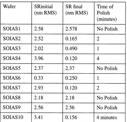
A complete summary of the AFM results is given below in Tables 5.1-5.4: Table 5.1: SOIAS WAFERS BEFORE TOUCH POLISH
Lateral
RMS (nm- Lateral
Wafer RRa (nm) Wavelength
(microns) 2 (SOIAS) 2.84 2.19 0.334 3 (SOIAS) 1.63 1.29 0.505 4 (SOIAS) 3.02 1.91 0.334 5 (SOIAS) 2.18 1.72 0.25 6 (SOIAS) 2.64 2.22 0.334 7 (SOIAS) 2.66 1.92 1.0 8 (SOIAS) 2.18 2.18 0.334 9 (SOIAS) 3.09 2.40 1.0 10 (SOIAS) 3.71 2.39 0.334
NanoSoope Ta"ppi AFN Soan size I.o000 o
Stpoint 0.51G9 U Scan rto 2.001 H Mu..her of sampie 20 SR=O.132 nm-RMS 1 0.2o Inl,"'dU 25.000 r./dil
Table 5.2: SOIAS WAFERS and SOI WAFERS AFTER TOUCH POLISH
Lateral Time of
WAFER rms) RA (nm) Wavelength Polish
(microns) (minutes) 2 (SOIAS) 0.089 0.074 1.0 2 3 (SOIAS) 0.486 0.359 0.334 1 4 (SOIAS) 0.123 0.096 1.0 4 5 (SOIAS) 2.18 1.72 0.334 NONE 6 (SOIAS) 0.25 0.193 0.505 1 7 (SOIAS) 0.196 0.147 0.333 2 8 (SOIAS) 2.18 2.18 0.334 NONE 9 (SOIAS) 3.087 2.401 1.0 NONE 10 (SOIAS) 0.156 0.137 0.334 4 3s (SOI) 0.132 0.108 1.0 4 4s (SOI) 0.134 0.109 1.0 4 5s (SOI) 0.224 0.177 0.33 NONE 6s (SOI) 0.222 0.180 0.33 NONE
Table 5.3: Percent Change of Morphology Parameters (+/- Increase/ Reduction)
Lateral Time Touch
WAFER RMS (%) RA (%) Wavelength PolishPolish
(%)
2 (SOIAS) -75 -96.63 98 2 3 (SOIAS) -70.18 -72.17 0 1 4 (SOIAS) -80.4 -94.97 300 4 6 (SOIAS) -75 -88.74 -49.5 1 7 (SOIAS) -96.86 -89.78 -66.7 2 10 (SOIAS) -50.8 -93.24 51.2 4 3s (SOI) -41.07 -41.07 203 4 4s (SOI) -38.42 -67.16 203 4300 r
Figure 5.23: Percentage Change of Morphology Parameters With Polish Time
Table 5.4 shows the effect of pirahna and HF clean on the morphology is negligible, and can only improve the morphology:
get better than before the clean.
Table 5.4: Piranha, Pirahna+HF Effect on Morphology Lateral Condition RMS (nm) RA (nm) Wavelength (microns) Original 0.394 0.270 0.334 Pirahna 0.222 0.178 0.505 (3: 1H2S0 4: H202) Pirahna 0.222 0.178 0.505 (3: 1H2S0 4: H202) Pirahna 0.219 0.173 0.505 (3:1H 2SO4: H202) 2 50H .. . . . .. . . ... x Percent Reduction Ra
o Percent Increase Lateral Wavelength
* Percent Reduction RMS ........ .........t i. .. ... .. ... ..
..
.
.
.
.
.
.
.
.
.
.
.
.
.
q
.
.
.
.
.
...
.
.
.
.
.
.
.
.
.
.
...
.
.
.
.
.
.
.
.
..
...
.
.
.
.
.
.
.
.
.
.
.
.
.
.
.
.
.
.
.
.
.
.
.
- -- I I --- -- I -- - 1 q - -I ........... .. .. ............... pT -10.5 2 . 1.5 2 2.5Time of Polish, minutes 150
Table 5.4: Piranha, Pirahna+HF Effect on Morphology Lateral
Condition RMS (nm) RA (nm) Wavelength
(microns)
Pirahna+HF 0.183 0.146 0.505
5.3
Discussion of AFM Results
The tables show the unifying feature that the morphology after the CMP is strongly depen-dent on the initial morphology of the wafer. This is demonstrated since we attain different values for morphology parameters at the same CMP conditions, where the only variable that is changing is the time of the touch polish. This statement assumes that the CMP experimental conditions remain approximately constant.
5.3.1 RMS Value
From Figure 5.23, we observe that the RMS value remains about the same for all times. There is a very slight reduction in RMS as we go from the 1 minute polish to the 2 minute polish. However, when we move to the 4 minute polish, the surface roughness became slightly less. As we move from SOIAS2 to SOIAS10, where SOIAS2 received 2 minutes of touch polish, and SOIAS10 received 4 minutes, we see that the change in RMS is reduced. The main difference between the morphology of the two wafers is that SOIAS2 has a smaller RMS roughness than SOIAS10 to start (2.84 nm compared to 3.71 nm). Also, the morphology of SOIAS2 has a larger wavelength so it is less "bumpy" on a lateral scale. The data shows that increasing the touch polish by 2 minutes slightly deteriorates the change in rms, indicating that every wafer needs to be treated individually in order to get required results. It shows that a rougher surface and a surface that is laterally more varying needs a longer touch polish time to reduce the RMS value.