HAL Id: tel-02159409
https://tel.archives-ouvertes.fr/tel-02159409
Submitted on 18 Jun 2019HAL is a multi-disciplinary open access archive for the deposit and dissemination of sci-entific research documents, whether they are pub-lished or not. The documents may come from teaching and research institutions in France or abroad, or from public or private research centers.
L’archive ouverte pluridisciplinaire HAL, est destinée au dépôt et à la diffusion de documents scientifiques de niveau recherche, publiés ou non, émanant des établissements d’enseignement et de recherche français ou étrangers, des laboratoires publics ou privés.
Development of compensated immersion 3D optical
profiler based on interferometry
Husneni Mukhtar
To cite this version:
Husneni Mukhtar. Development of compensated immersion 3D optical profiler based on interfer-ometry. Optics / Photonic. Université de Strasbourg, 2018. English. �NNT : 2018STRAD017�. �tel-02159409�
UNIVERSITÉ DE STRASBOURG
LogoEcole doctorale
ÉCOLE DOCTORALE n
o269 : Mathématiques, Sciences de l’Information et de
l’Ingénieur (MSII)
Laboratoire des Sciences de l’Ingénieur, de de l’Information et de l’Imagerie (ICUBE
UMR 7357)
THÈSE
présentée par :Husneni MUKHTAR
soutenue le : 29 Juin 2018
pour obtenir le grade de :
Docteur de l’université de Strasbourg
Discipline / Spécialité : Electronique, microélectronique, photonique
Development of compensated immersion 3D
optical profiler based on interferometry
THÈSE dirigée par :
Dr. MONTGOMERY Paul Directeur de recherche, CNRS, ICube (Strasbourg)
RAPPORTEURS :
Dr. GORECKI Christophe Directeur de recherche, CNRS, FEMTO-ST (Besançon)
Pr. SERIO Bruno Professeur des Universités, Université Paris Ouest, LEME (Paris)
AUTRES MEMBRES DU JURY :
Acknowledgements
Undertaking this PhD has been a truly life-changing experience for me and it would not have been possible to do without the support and guidance that I received from many people and the institutions.
First of all, I gratefully acknowledge my PhD supervisor, Paul Montgomery, senior CNRS researcher. Thank you for his professional guidance, advice, enormous encouragement, and continuous support of my research progress in this tough subject. Then I would like to thank Freddy Anstotz, my co-encadrant for his patient guidance, the discussion time and help in the instrumentation aspects. I have been extremely lucky to have them who cared so much about my work and responded to my questions and queries so well.
I would like to extend my gratitude to the permanent staff in the IPP group: Pierre Pfeiffer for helping me do some measurements with other microscopes, as well as Patrice Twardowski, Joël Fontaine and Sylvain Lecler.
I also would like to thank the IPHC team: Rémi Barillon for his support, Catherine Galindo for providing the colloid samples and discussions and Christophe Hoffman for helping me to improve the software performance of the motor controller. Thanks are also extended to Anne Rubin (ICS) for the idea of using PDMS.
Then I want to show my appreciation for the help from the engineers and technicians of ICube and the C3-Fab platform: Sébastien Shmitt for discussing the mechanical parts, Florent Dietrich for making the polymer molds and other mechanical parts used in the modification phase, Stephan Roques for making the Al step Si sample and guiding me in making the PDMS slabs, Nicolas Zimmerman for helping me in the chemical experiments and Nicolas Collin.
I extend my thanks to all the PhDs and post-docs in our research group, especially for Stephane Perrin, Audrey Leong-Hoi, Rémy Claveau, Gianto Gianto, and Eric Halter for your kind helps and great discussion. It has really been an enjoyable and unforgettable working and learning experience with all of them.
I would like to thank the LPDP (Indonesia Endowment Fund for Education), not only for providing the funding which allowed me to undertake this PhD, but also for giving me the opportunity to attend conference. Thanks are extended to Telkom university for permit and support me to continue my education in PhD.
I express my gratitude for my late father who always encourage and motivate me in the education and life. Thanks also all families and friends for their pray and moral support, particularly for my sister Sheizi Prista Sari for all her spirit and beliefs.
Finally, I thank Kusnahadi Susanto for his great daily support and make things easier in any perspective.
ii
TABLE OF CONTENTS
Acknowledgements ... 1
TABLE OF CONTENTS ... ii
TABLE OF TABLES ... v
TABLE OF FIGURES ... vii
TABLE OF ANNEXES ... xvi
TABLE OF ABBREVIATIONS AND ACRONYMS ...xvii
RÉSUMÉ ... xviii
INTRODUCTION ... 1
CHAPTER 1 ... 4
3D SURFACE PROFILING ... 4
1.1 Existing measurement systems... 5
1.1.1 Contact profilometers ... 6
1.1.2 Optical profilers ... 14
1.1.3 Comparison of characteristic parameters of profilers ... 20
1.2 Interference microscopy ... 22
1.2.1 Phase Shifting Microscopy ... 24
1.2.2 CSI method ... 26
1.2.2.1 General principle of CSI ... 27
1.2.2.2 Signal processing in CSI ... 27
1.3 Resolution ... 29
1.3.1 Lateral Resolution ... 29
1.3.2 Axial Resolution ... 32
1.4 Conclusion ... 33
1.4 Résumé de chapitre 1 ... 35
CHAPTER 2 ... 38
OPTIMIZATION OF A LINNIK MICROSCOPE ... 38
2.1 Linnik Setup ... 39
2.2 Linnik designs ... 40
2.3 Compact system vs breadboard... 45
2.4 Conclusion ... 46
2.5 Résumé du chapitre 2 ... 46
iii
WATER IMMERSION LINNIK HEAD AND COMPENSATION ... 49
3.1 Introduction ... 50
3.2 Initial Fogale microscope ... 52
3.2.1 Instrumentation description ... 52
3.2.2 Description of control and analysis software ... 54
3.2.3 Discussion ... 55
3.3 Modification of Fogale microscope... 55
3.3.1 Initial Fogale to Mirau setup ... 55
3.3.1.1 Instrumentation modification ... 56
3.3.1.2 Description of “FringeSurf 3D 3.1” control and analysis software and of “MountainsMap” surface roughness analysis software ... 56
3.3.1.3 First measurements using the Mirau Fogale ... 57
3.3.2 Mirau to Linnik in air ... 60
3.3.2.1 Instrumentation modification ... 60
3.3.2.2 Problems to solve to achieve the first measurements ... 61
Problem of OPD to find fringes... 62
Difficulties associated with the white LED light source ... 62
3.3.2.3 Description of Linnik head and the new integrated control software ... 69
3.3.3 Immersion linnik head and water compensation ... 70
3.3.3.1 Instrumentation modification ... 70
3.3.3.2 Compensation in mirror arm ... 70
3.3.3.3 First measurement with immersion Linnik setup ... 74
3.3.3.3.1 Measurements with no reference arm compensation ... 75
3.3.3.3.2 Measurements with reference arm compensation ... 81
3.3.4 Linnik using motor in mirror arm ... 84
3.3.4.1 Introduction ... 85
3.3.4.2 Description of motor control software ... 85
3.3.4.3 Measurement tests of the motorised stage ... 87
3.4 Comparison of measurements using water-‐immersion Linnik Fogale and other microscopes ... 87
3.5 Discussion of measurement results ... 94
3.5.1 Hardware misalignment ... 94
3.5.2 Resolution limit and loss in resolution ... 103
3.6 Conclusion ... 104
3.7 Résumé du chapitre 3 ... 105
CHAPTER 4 ... 107
SURPASSING THE DIFFRACTION LIMIT USING MICROSPHERE ASSISTED 3D IMMERSION MICROSCOPY ... 107
4.1 Introduction ... 108
iv
4.3 Measurements using microspheres ... 110
4.5 Discussion ... 119
4.6 Conclusion ... 120
4.6 Résumé du chapitre 4 ... 120
CONCLUSION AND PERSPECTIVES ... 122
BIBLIOGRAPHY ... 124
LIST OF PUBLICATIONS AND COMMUNICATIONS ... 133
v
TABLE OF TABLES
Table 1. The classification of methods for measuring surface texture based on ISO
25178-6 2010 [8]. ... 5
Table 2. Comparison the main characteristic parameters of stylus profiler, SPM, confocal microscope and white light interferometer [9]. ... 21
Table 3. Classification of 3D optical sensors [8]. ... 22
Table 4. Comparison of using different techniques in interferometer. ... 24
Table 5. The lateral resolution criteria based on the illumination type. ... 31
Table 6. Comparison of compact system and breadboard ... 45
Table 7. Comparison of white light LED and conventional halogen source. ... 64
Table 8. Specification of the comparative microscopes ... 87
Table 9. Comparison of measurements of etched silicon area-1 using each microscope ... 89
Table 10. Comparison of measurements of etched silicon area-2 and area-3 using each microscope ... 90
Table 11. Comparison of measurements of etched silicon (oval pattern) using each microscope. ... 91
Table 12. Comparison of measurements of etched silicon (oval pattern) using each microscope. ... 93
Table 13. Comparison of measurements of etched silicon (oval pattern) using each microscope. ... 93
Table 14. Mean of the lateral shift between successive images for each case and objective magnification. ... 99
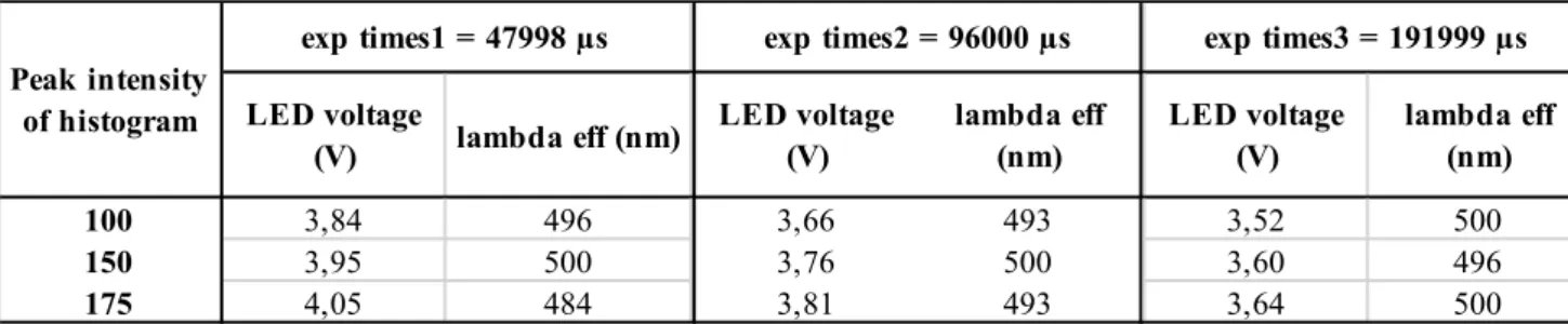
Table 15. Character of red LED with variance of LED voltage and exposure times in effect for the effective wavelength. ... 68
Table 16. Character of white light LED with variance of LED voltage and exposure times in effect for the effective wavelength. ... 68
Table 17. Comparison of measurement results of etched-silicon, hole area-2 using Zygo, Fogale, AFM and microspheres. ... 112
Table 18. Comparison measurement result of etched-silicon the hole area-3 using Zygo, Fogale, AFM and microspheres. ... 113
vi Table 19. Comparison of measurement results of etched silicon sample using the Zygo, Fogale, AFM and microsphere. ... 115 Table 20. Comparison of measurement result of grating sample using Zygo, Fogale, AFM and microsphere. ... 116 Table 21. Measurement results of standard grating SiMETRICS using BTGMS in range 30-45 µm. ... 119 Table 22. Measurement results of standard grating SiMETRICS using BTGMS microsphere in range 75-90 µm. ... 119
vii
TABLE OF FIGURES
Figure 1. Schematic of stylus profiler with LVDT as the motion detector. Part a is a fixed stylus with LVDT assembly and b is a sample. ... 6 Figure 2. Illustration of stylus profiler scanning over the surface of trenches with various aspect ratios. The convolution of a 25 µm radius stylus tip with a surface profile [9]. ... 7 Figure 3. (a) The schematic view of STM; Two typical modes of STM: (b)
constant-current mode, and (c) constant-height mode [19]. ... 9 Figure 4. The force F in the contact mode and the force gradient F’ in the con-contact mode is measured during scanning. The deflection sensor detects the deflection of the cantilever [21]. ... 10 Figure 5. Schematic of signal detection in AFM Tapping Mode. The probe is kept at a constant level above the sample, which results in a constant amplitude signal. Changes in the amplitude of the signal indicate that the distance between cantilever and object has changed [9]. ... 11 Figure 6. Schematic of variations of detection systems [21]. ... 11 Figure 7. An experimental scheme of a scanning force microscopy liquid cell of RNA polymerase [36]. A volume of 30 µl distilled water and some variations of other buffer types filled the chamber via the hosting and syringe. It took several minutes to 2 hours to reach the mechanical and thermal stability before performing imaging. ... 12 Figure 8. Illustration of high speed atomic force microscopy head integrated with OBD system [29]. ... 13 Figure 9. Illustration of two designs of immersion AFM in open (a) and closed (b) liquid cells [41]. ... 14 Figure 10. Simplified schematic of a confocal scanning optical microscope showing the sample (a) in the focal plane of the objective and (b) out of focus. (c) The schematic of chromatic confocal microscopy [1][9]. ... 16 Figure 11. White light interferograms for a spherical object as obtained for a few positions of the objective during an axial scan [9]. ... 17 Figure 12. The objective setups of (a) Michelson and (b) Mirau: MO (microscope objective), RM (reference mirror), BS (beam splitter). ... 17 Figure 13. (a) IMI system (b) Layout of SIMI system with two-camera arrangement. . 18 Figure 14. Principle of digital holographic microscopy [50]. ... 20
viii Figure 15. Superposition illustrations. (a) constructive interference, (b) destructive
interference, (c) constructive interference from a coherent light source ... 23
Figure 16. Phase determination, from 4 discrete steps of 120° [58]. ... 25
Figure 17.The technique of the change of phase [58]... 26
Figure 18. An interferogram on a surface using CSI. ... 27
Figure 19. Z-scan technique. ... 28
Figure 20. A circular aperture of Airy pattern in central Airy disk. ... 32
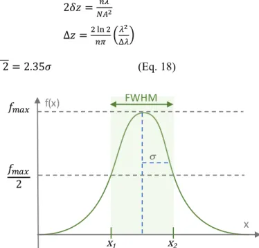
Figure 21. Illustration of a full width at height maximum and the relation with the standard deviation, s. ... 33
Figure 22. Linnik configuration in air. ... 39
Figure 23. Configuration of a Linnik water-immersion objective. ... 40
Figure 24. Experimental setup of a Linnik for FF-OCT imaging in living tissue [84]. . 41
Figure 25. Schematic of (a) the ultrahigh-resolution full-field OCT setup [7] and (b) the experimental setup of FF-OCM [86]. MO, microscope objective; BS, beam-splitter cube; DM, dichroic mirror; PZT, piezoelectric actuator. ... 42
Figure 26. General scheme of a high precision Linnik interferometer. working distance (WD), the axial objective lens distance (OLD) [85]. ... 43
Figure 27. Schematic of Linnik setup. ND, neutral density filter; GP, glass plate; DAQ, data acquisition board in computer [89]. ... 44
Figure 28. The system of Leitz-Linnik microscope developed at ICube [92]. ... 45
Figure 29. Illustration of combining CSI technique and ATR-FTIR. ... 51
Figure 30. Details of the initial Fogale Nanotech microscope in 2014 showing (a) the microscope mounted on old optical benches on the vibration isolated table and (b) the previous Linnik immersion head [94] with (1) LED light source, (2) beam splitter, (3) reference mirror assembly consisting of an adapted Mirau mechanism, (4) orientation adjustment and (5) the immersion objectives... 52
Figure 31. Details of the previous immersion head for the in situ characterization of the growth of HA layers in SBF solution, showing (a) the schematic layout, (b) the immersion head immersed in SBF solution and (c)the inside of the Teflon bath with the immersion objective, the water and the observation window [94]. ... 53
Figure 32. Interface software “FringeSurf 3D 2.1” for measuring the surface roughness (2013). ... 54 Figure 33. The first step of the modifications from (a) the initial Fogale Linnik microcope design on the old steel optical bench column (1) to (b) the Mirau
ix objective setup on the new aluminium optical bench column (1) and the head (2). The tip/tilt mechanism is indicated at (3). ... 56 Figure 34. The control and analysis software “FringeSurf 3D 3.1” for measuring surface roughness with the Mirau Fogale microscope (2014). ... 57 Figure 35. The first fringes were found for testing the Mirau Fogale using the red LED. The contrast and spacing are changed by using the adjustment screws in the Mirau mechanism... 58
Figure 36. The altitude and 3D images of DOE using the ´10 Mirau Fogale head with
the red LED, leff = 640 nm, dynamic range 15 µm, and step height 0.078 µm
[4415]. ... 58
Figure 37. Line profile of the measured area of DoE using the ´10 Mirau Fogale head
with the red LED, leff = 640 nm, dynamic range 15 µm, and step height 0.078 µm
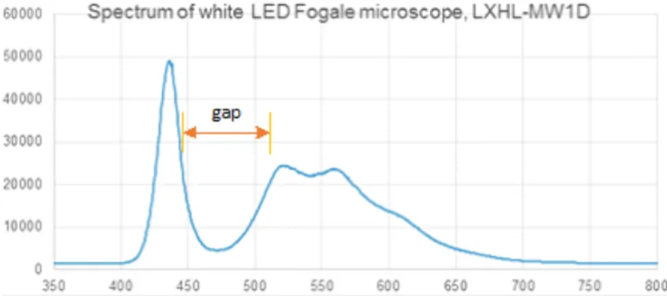
[4415]. ... 59 Figure 38. The altitude and 3D images of C-S-H colloid using the ´10 Mirau objective and the Fogale head with the red LED [4433]. ... 59 Figure 39. Line profile of the measured area of C-S-H colloid on the line using ´10 Mirau Fogale head with the red LED [4433]. ... 59 Figure 40. Illustration of the modification of the Linnik head. The tip/tilt and centering mechanism (1) is moved from the object to the reference arm and the beam stopper (2) and 8 mm-thick ring (3) are moved from the reference arm to the object arm. An adaptor tube (4) is used to mount the Mirau mirror mechanism on the reference arm. An adapted back plate (5) and an adapted cube holder (6) are installed on the rear side of the Linnik head mounted on the microscope. ... 60 Figure 41. The objective tip/tilt and centering mechanism. The screws marked by red circles are used to change the angle of the objective in order to change the fringe orientation separation. ... 61 Figure 42. Adjustment control in reference arm. ... 61 Figure 43. First fringes found by ´20 (immersion objectives) Linnik Fogale in air with red LED (left) and white LED (right) illumination. ... 62 Figure 44. The asymmetrical envelope of an interferogram using the original white LED LXHL-MW1D. ... 63 Figure 45. The measured spectrum of the original phosphor-based white LED
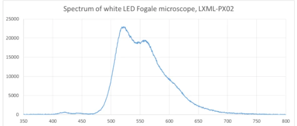
LXHL-MW1D of the initial Fogale microscope. ... 63 Figure 46. The measured spectrum of the new white LED (LUXEON Rebel lime color) chosen for its more balanced spectral range. ... 64
x
Figure 47. Three dominant ways to produce white light based on LEDs [102]. ... 65
Figure 48. Several ways to generate white light based on LEDs implemented with di-, tri-, and tetra chromatic white sources [103]. ... 65
Figure 49. Spectral power distributions of several types of LEDs. ... 66
Figure 50. Comparison of the spectrum of ideal sunlight with two LED-based white-light sources. ... 66
Figure 51. Spectral power distributions of early phosphor-based white LEDs (left), and white LEDs using more developed phosphors (right, in 2003) with increased output between 600 and 650 nanometers... 67
Figure 52. Interface software “CSI-2015” for measure the surface roughness on the Linnik Fogale microscope. ... 69
Figure 53. Experimental arrangement of water-immersion Linnik head. BS, beam splitter (broadband, nonpolarizing); MO, microscope objective (water immersion); RM, reference mirror (80% reflectivity); PZT, piezo translation. ... 70
Figure 54. The schematic of how a correction collar works [106]. ... 71
Figure 55. Samples of water retaining SPA polymers in the bubble shape. ... 72
Figure 56. Use of SPA beads in the mirror arm (a) and in the object arm (b). ... 72
Figure 57. Design (right) and mold plate (left) for making PDMS slabs in various heights to suit the working distance of the objective... 73
Figure 58. (a) An second improved mold design of PDMS made of Teflon with a glass plate forming the base of the mold, (b) PDMS contacts with reference mirror. ... 73
Figure 59. Some PDMS slabs. ... 74
Figure 60. Difference focus positions of an aluminium layer on silicon sample placed under the sample objective with the thickness of PDMS slabs of (a) 3.4 mm, (b) 3.5 mm and 3.6mm; using ´20 immersion objective with a working distance of 3.6 mm. The best focus is (b). ... 74
Figure 61. Comparison of fringe images of Al step on Si using red LED, ´20 immersion Linnik objectives in (a) air (0.05 step height, 26 dynamic range, 𝜆𝑒𝑓𝑓 = 640 nm, 4579); and (b) water (0.05 step height, 25 dynamic range, 𝜆𝑒𝑓𝑓 = 640 nm, [4580])... 75
Figure 62. Comparison of raw fringe signal on Al step on Si using red LED, ´20 immersion Linnik objectives in air (top) (0.05 µm step height, 26 µm dynamic range, 𝜆𝑒𝑓𝑓 = 640 nm, 4579); and water (bottom) (0.05 µm step height, 25 µm dynamic range, 𝜆𝑒𝑓𝑓 = 640 nm, [4580])... 76
xi Figure 63. Comparison of fringe signals and fringe envelopes on Al step on Si using red LED, ´20 immersion Linnik objectives in (a) air (0.05 µm step height, 26 µm dynamic range, 𝜆𝑒𝑓𝑓 = 640 nm, rectify, 4579); and (b) water (0.05 µm step height, 25µm dynamic range, 𝜆𝑒𝑓𝑓 = 640 nm, FSA interpolation, [4580]). ... 76 Figure 64. Comparison of fringe images of Al step on Si using red LED, ´40 immersion Linnik objectives in (a) air (0.05 µm step height, 21µm dynamic range, 𝜆𝑒𝑓𝑓 = 640 nm, 4584); and (b) in water (0.05 µm step height, 18 µm dynamic range, 𝜆𝑒𝑓𝑓 = 640 nm, [4585]). ... 77 Figure 65. Comparison of raw fringe signals on Al step on Si using red LED, ´40 immersion Linnik objectives in air (top) (0.05 µm step height, 21 µm dynamic range, 𝜆𝑒𝑓𝑓 = 640 nm, 4584); and water (bottom) (0.05 µm step height, 18 µm dynamic range, 𝜆𝑒𝑓𝑓 = 640 nm, [4585])... 77 Figure 66. Comparison of fringes signals and fringe envelopes on Al step on Si using red LED, ´40 immersion Linnik objectives in (a) air (0.05 µm step height, 21 µm dynamic range, 𝜆𝑒𝑓𝑓 = 640 nm, FSA interpolation, 4584); and (b) water (0.05 µm step height, 18 dynamic range, 𝜆𝑒𝑓𝑓 = 640 nm, FSA interpolation, [4585]). 78
Figure 67. Comparison of 3D images of Al step on Si using red LED, ´20 immersion
Linnik objectives in (a) air (0.05 µm step height, 26 dynamic range, 𝜆𝑒𝑓𝑓 = 640 nm, rectify, 4579); and (b) water (0.05 µm step height, 25 dynamic range, 𝜆𝑒𝑓𝑓 = 640 nm, FSA technique [4580]). ... 79
Figure 68. Comparison of 3D images of Al step on Si using red LED, ´40 immersion
Linnik objectives in air (top) (0.05 step height, 21 dynamic range, 𝜆𝑒𝑓𝑓 = 640 nm, 4584); and water (bottom) (0.05 step height, 18 dynamic range, 𝜆𝑒𝑓𝑓 = 640 nm, [4585])... 79 Figure 69. Comparison of the line profiles of the measured height of the Al step on Si using red LED, ´20 immersion Linnik head in air (shown in (a) and (c)) and in water (shown in (b) and (d)). The measurements of the step height (∆Z) of the sample are 2.49 µm (0.05 step height, 25 dynamic range, 𝜆𝑒𝑓𝑓 = 640 nm, FSA interpolation, [4580]). ... 80 Figure 70. Comparison of line profiles of the measured height of the Al step on Si using the 40x immersion Linnik head in air (shown in (a) and (c)) and in water (shown in (b) and (d)). The measurements of the step height (∆Z) of the sample are 2.49 µm ) (0.05 step height, 18 dynamic range, 𝜆𝑒𝑓𝑓 = 640 nm, [4585]). ... 80 Figure 71. Focus of the reference objective on reference mirror. An elastic polymer of (a) SPA and of (b) PDMS is placed between the reference mirror and the objective ... 81
xii Figure 72. Etched squares in silicon, 8 µm wide and 2.5 um deep measured with the ´40 water immersion Linnik system (NA=0.8, leff=450 nm) with SPA placed in the
reference arm showing (a) height image, (b) line profile from (a), (c) fringe image and (d) 3D image. ... 82 Figure 73. Etched squares in silicon, 8 µm wide and 2.5 um deep measured with the ´40
water immersion Linnik system (NA=0.8, leff=450 nm) with 3.25 mm thickness of
PDMS placed in the reference arm showing (a) height image, (b) line profile from (a), (c) fringe image and (d) 3D image. ... 82 Figure 74. Fringe image of Al step on Si using white light, ´20 immersion Linnik objectives in water (0.05 µm step height, 12 dynamic range, 𝜆𝑒𝑓𝑓 = 640 nm, [4634-5]). ... 83 Figure 75. (a) The raw fringe signal and (b) the fringe envelope on the Al step on Si using white light, ´20 immersion Linnik objectives in water (0.05 µm step height, 12 dynamic range, 𝜆𝑒𝑓𝑓 = 640 nm, [4634-5])... 83 Figure 76. Line profile of the measured height of the Al step on Si using ´20 immersion Linnik objectives with white light in water (0.05 µm step height, 12 dynamic range, 𝜆𝑒𝑓𝑓 = 640 nm, [4634-5]). The step height of Aluminum on Silicon (∆Z) and the measured lateral resolution (∆X) are 2.50 µm and 0.2 µm respectively. ... 84 Figure 77. Motorized control installed on block of the reference arm for adjusting the path length or reference arm. Images viewed in three sides are marked by red arrows (motor) and blue arrows (adapted plate). ... 85 Figure 78. Graphic user interface for controlling the stepper motor (created by Husneni Mukhtar & Christophe Hoffman, IPHC). ... 86 Figure 79. Flow-work of the interface for controlling the motorized stage in the reference arm. ... 86 Figure 80. Results of measuring an etched silicon grating sample in water using the ´20 immersion Linnik Fogale microscope with the white light LED after motorized positioning of the OPD, showing the altitude image, a line profile and the 3D results [4701-4]. ... 87 Figure 81. Etched Silicon hole area-1, is measured by: (first row) the Zygo microscope
in air (´50 Mirau, NA=0.55); (second row) the Fogale Linnik water immersion
system (´40, NA=0.8, 0.056 µm step height, 5.5µm dynamic range, leff=450 nm,
[4721]); and (third row) the Fogale Linnik water immersion system (´20, NA=0.5, 0.056 µm step height, 10 µm dynamic range, leff=450 nm, [4637]). ... 88
Figure 82. Etched Silicon hole area-2 and area-3, measured by (first row) the Zygo microscope in air (´50 Mirau, NA=0.55,); (second row) Fogale Linnik water
xiii immersion system (´40, NA=0.8, 0,056 µm step height, 4.5µm dynamic range, leff=450 nm, [4721]); and (third row) AFM non-contact mode. ... 89
Figure 83. (a) The raw fringe signal and (b) the fringe envelope on the etched silicon sample no.16 h-3 using the Fogale immersion Linnik with the ´20 immersion objective and the white LED (0.05 µm step height, 9 dynamic range, 𝜆𝑒𝑓𝑓 = 450 nm, [4667a]). ... 90 Figure 84. Etched Silicon, oval pattern, is measured by (first row) the Zygo microscope
in air (´50 Mirau, NA=0.55); (second row) the Fogale immersion Linnik system in water (´40, NA=0.8, 0.056 µm step height, 6.3 µm dynamic range, leff=450 nm,
[4721]); (third row) AFM non-contact mode; and (fourth row) the Fogale Linnik immersion system in water (´20, NA=0.5, 0,056 µm step height, 14 µm dynamic range, leff=450 nm, [4675a]). ... 91
Figure 85. Etched Silicon grating pattern, is measured by (first row) the Zygo microscope in air (´50 Mirau, NA=0.55); (second row) the Fogale Linnik immersion system in water (´40, NA=0.8, 0.056 µm step height, 5 µm dynamic range, leff=450 nm, [4721]); (third row) the Fogale Linnik immersion system in
water (´20, NA=0.5, 0.056 µm step height, 10 µm dynamic range, leff=450 nm,
[4674]); and (fourth row) AFM non-contact mode. ... 92 Figure 86. 2 µm high Al step on Si is measured by (first row) the Zygo microscope in air (´50 Mirau, NA=0.55); and (second row) the Fogale Linnik immersion system (´20, NA = 0.5, 0.05 µm step height, 13 dynamic range, 𝜆𝑒𝑓𝑓 = 450 nm, rectify, [4644])... 93 Figure 87. Illustration of the problem of lateral image displacement during axial scanning over a dynamic range of 5 µm using the x20 immersion Linnik: (a) measured area of displacement test; (b) Line profile of the measured area on a stack of scanned images, with a zoom of a specific area. ... 95 Figure 88. Flowchart of proposed technique to measure the displacement of misalignment and to correct the image position. ... 95 Figure 89. Interface software “Image displacement analysis for CSI scanning” for checking and correcting the position of scanned images along the x- and y-axis caused by misalignment (created by H Mukhtar)... 96 Figure 90. Description of three cases to test and observe the effect of misalignment. .. 96 Figure 91. The lateral displacement in x in pixels between successive images over 100 steps using the cross-correlation function. The dynamic range is 5 µm, dZ = 0.056 µm, leff= 450 nm, for the x20 immersion objective. ... 97
xiv Figure 92. The shift along the x-axis between two images for each measurement using the cross-correlation function after 10´ pixel resampling by a cubic kernel interpolation. Dynamic range= 5 µm, dZ= 0.056 µm, leff= 450 nm, ´20 immersion objective. ... 98 Figure 93. The shift between successive images for each scanning step for the case of the x-axis. Dynamic range = 5 µm, dZ= 0.056 µm, leff= 450 nm for (a) ´20 immersion objective and (b) ´40 immersion objective. Dynamic range = 10 µm, dZ= 0.056 µm, leff= 450 nm for (c) ´20 immersion objective and (d) ´40 immersion objective... 98 Figure 94. The lateral image shift for a short dynamic range (2.5 µm) of each objective and case. ... 99 Figure 95. The continuity trend of the lateral image shift during axial scanning for larger values of dynamic range (2.5 µm, 5 µm, and 10 µm): (a),(c) using ´20 immersion objective for case 1 and case 2; (b),(d) using the ´40 immersion objective for case 1 and case 2. ... 100 Figure 96. The shift response for different step heights (dZ) over the same dynamic range, using the ´20 immersion objective. ... 100 Figure 97. The lateral image shift between two images for each scanning step and cases along the y-axis. The dynamic range= 5 µm, dZ= 0.056 µm, leff= 450 nm for (a) ´20 immersion objective and (b) ´40 immersion objective; The dynamic range =10 µm, dZ= 0.056 µm, leff= 450 nm for (c) ´20 immersion objective and (d) ´40 immersion objective... 101 Figure 98. Successive profiles of the grating for (a) before correction of the image shift measured in the same area using the ´20 immersion objective and (b) after correction of the image shift, 10 µm dynamic range and 0.056 µm step height. .. 102 Figure 99. The RS-N type resolution standard consists of a set of 9 gratings with different pitch values varying from 0.3, 0.4, 0.6, 0.8, 1.2, 2.0, 3.0, 4.0 and 6.0 µm. ... 103 Figure 100. Measurements of the RS-N type resolution standard using the ´40 immersion Linnik objective in water with the PSM technique (𝜆𝑒𝑓𝑓 = 505 𝑛𝑚). The grating sizes visible were (a) 0.8 µm; (b) 1.2 µm; (c) 2 µm; (d) 3 µm; (e) 4 µm; (f) 6 µm [4674b]. ... 104 Figure 101. Schema of the nano-3D interferometric microscope of Leitz Linnik in air [125]. ... 109 Figure 102. A microsphere-assisted interference microscopy. ... 110
xv Figure 103. Position of BTGMS on the sample using ´20 immersion Linnik Fogale microscope. The diameter of the microsphere is 67 µm, [4673b]. ... 111 Figure 104. Etched Silicon hole area-2 measured by ´20 immersion Linnik Fogale microscope, (first row) using a 67 µm BTGMS microsphere on it (0.05 step height,
10 dynamic range, 𝜆𝑒𝑓𝑓 = 450 nm, [4673b]); (second row) using a 64 µm-BaTiO3
microsphere on it (0.05 step height, 12 dynamic range, 𝜆𝑒𝑓𝑓 = 450 nm, [4667-c2]). ... 112 Figure 105. Position of 67 um BaTiO3 on the hole area-3 of etched Silicon, using ´20
immersion Linnik Fogale microscope. ... 113 Figure 106. Etched Silicon hole area-3 measured by ´20 immersion Linnik Fogale microscope, (first row) using a 67 µm BTGMS microsphere on it (0.05 step height, 14 dynamic range, 𝜆𝑒𝑓𝑓 = 450 nm, [4678]); (second row) using a 61.7 µm-BaTiO3 microsphere on it (0.05 step height, 10.5 dynamic range, 𝜆𝑒𝑓𝑓 = 450 nm,
[4681])... 113 Figure 107. Position of a 70 µm BTGMS on sample in water using Fogale microscope.
... 114
Figure 108. Etched Silicon on oval pattern measured by ´20 immersion Linnik Fogale
microscope using a 7 µm BTGMS microsphere on it (0.05 step height, 15.5 dynamic range, 𝜆𝑒𝑓𝑓 = 450 nm, [4675b]). ... 114 Figure 109. Position of a 71 µm BTGMS on the sample in water using the Fogale microscope. ... 115 Figure 110. Etched Silicon on grating pattern measured by ´20 immersion Linnik Fogale microscope using a 71 µm BTGMS microsphere on it (0.05 step height, 18 dynamic range, 𝜆𝑒𝑓𝑓 = 450 nm, [4674b]). ... 115
Figure 111. Standard grating SiMETRICS measured by ´40 immersion Linnik Fogale
microscope, red LED, 0.056 µm step height, 𝜆𝑒𝑓𝑓 = 530 nm in water: pitch 1.2 µm (11 dynamic range, using 43 µm BTGMS); pitch 0.8 µm (5 dynamic range, using 44 µm BTGMS); pitch 0.4 µm (6.5 dynamic range, using 45 µm BTGMS); pitch 0.3 µm (6.5 dynamic range, using 43 µm BTGMS), [4714]. ... 117
Figure 112. Standard grating SiMETRICS measured by ´40 immersion Linnik Fogale
microscope, red LED, 0.090 step height, 𝜆𝑒𝑓𝑓 = 505 nm in water: pitch 3 µm (11 dynamic range, using 80 µm BTGMS); pitch 2 µm (10 dynamic range, using 80 µm BTGMS); pitch 1.2 µm (10 dynamic range, using 82 µm BTGMS); pitch 0.8 µm (10 dynamic range, using 77 µm BTGMS); pitch 0.6 µm (10 dynamic range, using 77 µm BTGMS); pitch 0.4 µm (10 dynamic range, using 75 µm BTGMS), [4716]. ... 118
xvi
TABLE OF ANNEXES
Annex 1. Data sheet of the light source of initial Fogale, Lumileds LXHL-MW1D white
LED, 5500K, round ... 137
Annex 2. Data sheet of cube beam splitter of Fogale microscope ... 139
Annex 3. Specification of immersion objectives from Leica. ... 140
Annex 4. Design of the adapted tube for objective in reference arm. ... 141
Annex 5. Data sheet of white light LED (lime LED color) ... 142
Annex 6. The procedure of Abbe-refractometer ... 143
xvii
TABLE OF ABBREVIATIONS AND
ACRONYMS
AFM : Atomic Force Microscope ... 8, 12 ATR-‐FTIR : Attenuated Total Reflectance Fourier Transform Infrared spectroscopy ... 2, 50 BTGMS : Barium Titanate Glass microspheres ... 109, 116
CCI : Coherence Correlation Interferometry ... 21
CPM : Coherence Probe Microscopy ... 2, 21 C-‐S-‐H : calcium silicate hydrate ... 3, 57, 59 CSI : Coherence Scanning Interferometry ... 2, 25 CSM : Coherence Scanning Microscopy... 21
DHM : digital holographic microscopy... 19
DOE : diffractive optical element ... 57
FF-‐OCT : full-‐field optical coherence tomography ... 2, 28, 41 FFT : Fast Fourier Transform ... 27
FOV : field of view ... 19
FSA : Five Step Adaptive ... 28, 54 FWHM : full width at half maximum ... 29, 32 LED : light emitting diode ...41, 57, 62 LVDT : linear variable differential transformer ... 6
MEMS : microelectromechanical system... 5, 26 MOEMS : micro-‐opto-‐electro-‐mechanical system ... 5, 26 NA : numerical aperture ...29, 30, 32 OBD : optical beam deflection ... 13
OLD : Objective Lens Distance... 42
OPD : optical path difference ... 23, 24, 27, 61 PBS : polarizing beam splitter ... 41
PDMS : polydimethylsiloxane ...71, 72, 81 PFSM : peak fringe scanning microscopy ... 27
PSF : point spread function ...28, 29, 31 PSI : phase shifting interferometry ... 18
SBF : simulated body fluid ... 2
SIMI : Simultaneously Immersion Mirau Interferometry ... 18
SPA : sodium polyacrylate... 71, 80 SPM : Scanning Probe Microscopy ... 7, 11 STM : Scanning Tunneling Microscopy ... 8, 9, 12 SWLI : Scanning White Light Interferometry... 22
VSI : Vertical Scanning Interferometry ... 22
WD : Working Distance ... 42
WLI : white light interferometry ... 7 WLSI : White Light Scanning Interferometry... 2, 16, 21, 34
xviii
RÉSUMÉ
La profilométrie optique en microscopie interférométrie est une technique d'imagerie optique 3D bien établie permettant la caractérisation de surfaces d'une manière non-invasive, rapide et avec une résolution axiale nanométrique. Cette technique de mesure est parfaitement adaptée à la mesure de rugosité de surface pour des structures ou circuits microélectroniques, des éléments optiques diffractifs, des systèmes micro-électromécaniques (MEMS) ou des dispositifs de micro-fluidiques. L'Interférométrie en lumière blanche CSI (Coherence Scanning Interferometry, également connue comme White Light Scanning Interferometry, WLSI) est une technique basée sur la détection du pic ou de l’enveloppe de franges d’interférence. La technique utilise un échantillonnage des franges selon l'axe optique par l’acquisition d'une pile d'images XYZ. Le traitement d'image est ensuite utilisé pour identifier les enveloppes des franges, le long de l’axe Z pour chaque pixel afin de mesurer la position d’une surface unique ou de structures enterrées dans une couche. La mesure de la forme de la surface en CSI, nécessite un traitement basé souvent sur la détection d’un pic directement sur les franges ou sur l’enveloppe des franges après extraction de celle-ci à l’aide d’algorithmes de traitements implémentés voir développés dans notre équipe. Les avantages de la CSI sont la sensibilité axiale nanométrique, le champ de vision large (de quelques centaines de µm à plusieurs mm) et la vitesse de mesure (quelques secondes à quelques minutes selon les algorithmes ou leur plateforme d’implémentation).
Classiquement les microscopes interférométriques se limitent aux mesures des échantillons dans l’air. A l’instar de la microscopie 2D dans le domaine biologique, différents groupes de recherche cherchent à développer la microscopie interférométrique en milieu liquide. Le travail dans un milieu liquide permet, outre l’amélioration de la résolution latérale en microscopie optique, d’ouvrir le domaine d’application à l’étude d’échantillons nécessitant l’immersion dans de l’eau ou dans du sérum physiologique. Une demande croissante de mesures nanoscopiques en milieu liquide, comme l’étude de la croissance de couches d’hydroxyapatite sur des implants (dents, prothèses, …) ou plus particulièrement l’étude de couches de colloïdes pour l'étude de réactions chimiques.
Ce travail de thèse se fait dans le cadre du développement instrumental d’un microscope interférométrique de type Linnik en immersion à haute résolution axiale et fort grossissement. L’étude bibliographique a permis d’établir un état de l’art dans le domaine de la microscopie interférométrique en immersion. Elle a également permis de mettre en évidence les verrous scientifiques et technologiques à lever afin de réaliser un système opérationnel en immersion. Dans ces travaux sont présentés l’adaptation d’un interféromètre industriel construit par la société FOGALE pour la mesure en immersion et appliqué à la mesure de couches d’agrégats de colloïdes étudiées par le groupe de radiochimie de l’IPHC.
xix Le microscope FOGALE est architecturé autour d’une tête interférométrique de type Linnik classique. Un des verrous technologiques à résoudre lors du travail en immersion dans un interféromètre Linnik est la compensation du chemin optique dans le bras miroir lorsque le bras objet se trouve en immersion. La difficulté vient principalement de l’implémentation horizontale du bras miroir, ce qui rend difficile l’immersion du miroir dans le liquide.
Une première solution étudiée dans ce cas était l’utilisation et l’insertion de lamelles de verre entre l’objectif et le miroir. La difficulté d’insérer des verres adéquats en épaisseur et en indice ne permettait pas d’adapter les chemins optiques de façon optimale afin d’obtenir des franges de qualité dans le plan focal. Le contraste des franges ne permettait pas de réaliser des mesures de qualité avec une telle compensation. Il est également apparu un problème de réglage extrêmement délicat de l’interféromètre dû principalement à des problèmes de choix de construction limitant les réglages fins et l’alignement précis des éléments optiques mais également au choix du nombre de degrés de liberté (rotations et translations) de certains éléments du système.
Dans une seconde phase et afin de pouvoir réaliser des tests et des mesures sur les premiers échantillons, nous avons adapté un objectif interférométrique compact de type Mirau pour les mesures dans l'air. Les principaux inconvénients d’une telle solution sont le grossissement et la résolution limitée que l’on peut obtenir avec de tels types d’objectifs et la difficulté de les faire fonctionner en immersion. Le travail de thèse s’est donc concentré principalement sur la levée des différents verrous pour développer une structure d’interféromètre Linnik utilisable et réglable dans des conditions d’expérimentation acceptable par l’utilisateur final.
Une première étude a donc consisté à trouver et à modifier les systèmes de réglage mécanique afin de garantir l’ensemble des degrés de liberté afin de permettre un réglage optimal du Linnik. Le réglage du bras miroir a été motorisé afin de faciliter la recherche des franges dans le plan focal de l’objectif. Le contrôle de cet actionneur est développé sous LabView. Il permet la recherche aisée des franges d’interférence. Ce système pourra évoluer dans le futur par l’implémentation d’un algorithme de recherche automatique des franges en intégrant un système de reconnaissance et de détection des franges grâce à la caméra associée à un traitement développé sous LabView.
Une seconde partie est consacrée à l’étude des solutions de compensation du chemin optique entre le miroir de référence et son objectif. Une étude des différentes solutions possibles de compensation a été réalisée. Deux solutions prometteuses ont été testées et mis en œuvre qui évite utilisation d’eau liquide ou un repliement vertical du bras de référence. La première solution est basée sur l’utilisation de billes de polyacrylate de sodium (SPA). Cette solution utilise les propriétés des polymères de polyacrylate de sodium à absorber de très grande quantité d’eau et leur confère ainsi un indice de réfraction très proche de l’eau. Les caractéristiques optiques sont donc très proches. Les
xx résultats de mesure sont présentés et ont permis de montrer la viabilité de cette solution. La mise en œuvre des billes de SPA est relativement simple et peu chère. L’inconvénient est la durée d’utilisation qui est limitée à une journée voir quelques heures et causée par l’évaporation de l’eau du polymère.
La seconde solution consiste à utiliser des pastilles de PDMS moulé sur mesure pour notre application. Pour cela un moule fut conçu et fabriqué en téflon. Une caractéristique indispensable de ces pastilles est, outre les caractéristiques optiques (qualité, indice, …), l’élasticité ou la souplesse indispensable pour éviter une déformation du miroir de référence lors de l’assemblage sur l’objectif de référence. Un ensemble de mélange et un procédé d’élaboration a dû être développé pour atteindre des performances acceptables. Si les résultats sont prometteurs, il reste cependant encore à optimiser la qualité optique de ces éléments afin d’augmenter la qualité des franges d’interférences. Ces techniques de compensation ont été appliquées à notre banc de mesure et pour deux grossissements de jeux d’objectifs à immersion en X20 et X40. Une campagne de caractérisation du microscope a été menée et les résultats sont présentés dans la thèse sur des échantillons de référence et en immersion. Ces mesures sont comparées à des mesures sur des appareils de référence comme des mesures en AFM ou sur le système de mesure interférométrique commercial Zygo disponible sur notre plateforme de caractérisation. Enfin les premières mesures sur des échantillons en immersion de couches de colloïde sont présentées et ont permis de valider le microscope interférométrique en immersion.
Le cadre du projet de thèse se situe dans une collaboration avec le Professeur Rémy Barillon et le groupe de radiochimie du Département Recherches Subatomiques (DRS) de l’IPHC (Institut Hubert Curien). Le but est de développer un système de CSI en immersion pour le combiner avec la spectroscopie FTIR dans l'analyse de couches de colloïdes en immersion pour étudier les polluants dans le sol.
2 Coherence Scanning Interferometry (CSI) is a non-contacting 3D optical profilometry technique that is increasingly used for measuring the roughness and shape of microscopic material and component surfaces [1], such as microelectronic structures, miniature optical elements, micro-electro-mechanical systems and micro-fluidic devices. The technique is also known as White Light Scanning Interferometry (WLSI) or Coherence Probe Microscopy (CPM). The particular advantages of CSI are nanometric axial sensitivity (1 nm), a wide field of view (hundreds of µm to several mm) and high speed of measurement (several seconds to several minutes).
Classically, measurements are limited to dry surfaces in air that are static. In more recent research projects, several new modes of measurement have also been developed: the strobed technique for periodically moving surfaces [2], the 4D microscopy real time mode for measuring aperiodically moving or changing surfaces at a rate of up to 25 3D images per second [3], the tomographic mode, or full-field optical coherence tomography (FF-OCT) for measuring transparent complex layers [4] and the local spectroscopy mode for measuring local optical properties [5].
In the present project, we are interested in being able to study samples in liquids, such as in the case of chemical reactions or biological samples. In order to be able to measure such samples, several challenges need to be overcome such as making a system that works correctly in liquids and developing techniques to compensate for the dispersion mismatch and optical aberrations between both interference arms when imaging samples in a liquid medium or inside tissue or living cells, etc.
The objectives of this PhD research project are to extend the measurement modes [6] of the CSI technique to be able to cope with samples in a liquid medium at high speed using a fringe scanning system by developing an immersion interferometer head based on the Linnik interferometer using immersion objectives.
One area of interest for the application of the new technique will be in the in-situ characterization of the chemical exchange in thick layers of colloids for environmental applications in combination with Attenuated Total Reflectance Fourier Transform Infrared spectroscopy (ATR-FTIR, in collaboration with the team of Rémi Barillon, IPHC, Strasbourg). Another area of application is in the study of the growth of layers of synthetic biomaterials such as hydroxyapatite (the mineral part of bones and teeth) in simulated body fluid (SBF), an important material used in human implants [3] [8]. The technique could also be used in the analysis of the properties of the surface and sub-surface region of the skin in order to help in identifying different skin disorders [7]. The manuscript consists of four main chapters and is organized in the following way. In the first chapter, we give a summary of several existing surface profiling techniques by presenting the principle work, the utilities and a comparison between them. This demonstrates the usefulness of interference microscopy for many types of measurements, with its high axial and lateral resolutions and other advantages. After
3 having recalled the interest of interference microscopy compared with other optical profilers, we then present the state of the art of the two methods widely used and the lateral and axial resolutions.
The second chapter presents the different Linnik setups that exist, including their measurement performance in air and liquid. In this way, it is demonstrated that the immersion Linnik system has a high potential for improving the lateral resolution of surface roughness measurement and being able to measure samples in a liquid medium. The different challenges for designing the Linnik interferometer are presented, showing the need for path length compensation in the reference arm.
The third chapter is devoted to the overall work that has been performed to adapt a commercial (Fogale Nanotech) Linnik microscope to be able to work in the immersion mode. We begin by introducing the conditions of the initial system. This is then continued by illustrating in sequence the modification steps of this initial system to achieve the water immersion Linnik. Each modification step presents the description of the instrument, the measurement tests carried out and discussion. The presentations cover the work carried out on studying the different solutions for path length compensation using self-supporting polymers. The system is tested with measurements on calcium silicate hydrate or C-S-H colloids on Ge substrate and some patterns of etched Silicon. The result comparison is also carried out with other microscopes. A specific section of the discussion is presented to discuss the specific problems encountered during the work.
In the fourth and final chapter, the new immersion system is tested with the recently discovered microsphere assisted microscopy technique that allows a considerable improvement in the lateral resolution, or the effect of "super-resolution". Test samples of etched Si samples measured with barium titanate microspheres (64 µm to 71 µm in diameter) combined with CSI technique in water show an improvement in additional magnification up to 3.01 times. Then test samples of standard grating from SiMETRICS measured with barium titanate microspheres (43 µm to 82 µm in diameter) combined with Phase Shifting Microscopy (PSM) technique in water show an improvement in lateral resolution from 800 nm with the immersion objective alone to 300 nm with the microsphere. This demonstrates the high potential of the immersion Linnik for very high resolution optical measurements of surface roughness and structures.
4
CHAPTER 1
3D SURFACE PROFILING
5
1.1 Existing measurement systems
The measurement of microscopic surface roughness and 3D surface structures is an important field of materials development and industrial metrology and inspection. Measurement techniques are required for characterizing new materials, microelectromechanical system and micro-opto-electro-mechanical system (MEMS and MOEMS) as well as traditional materials such as metallic surfaces, paper and plastics. In ISO 25178 part 6 (2010), three classes of methods of instruments for measuring surface texture are defined as shown in Table 1. These consist of the 2D graph or profile of the surface topography method, represented mathematically as a height function, z(x); the topographical surface image of the surface measurement method, represented mathematically as a height function, z(x,y); and the representative surface area of the surface measurement method of which the numerical results produced depend on the area-integrated properties of the surface texture. This last method will not be discussed in this thesis. The various techniques for contact profilometers and optical profilometers to measure the surface topography are now described in this section.
Table 1. The classification of methods for measuring surface texture based on ISO 25178-6 2010 [8].
Angle Resolved Scatter Angle Resolved SEM
Circular Interferometric Profiling Coherence Scanning Interferometry Confocal Chromatic Microscopy Confocal Microscopy
Contact Stylus Scanning Digital Holography Microscopy Focus Variation Microscopy Optical Differential profiling Parallel Plate Capacitance Phase Shifting Interferometry Pnematic
Point Autofocus Profiling Scanning Tunneling Microscopy SEM Sterescopy
Structured Light Projection Total Integrated Scatter
Table 1
Profiler method Linear profiling (senses Z(X) Areal topography Senses Z(X,Y) or Z(X) as function of Y
6
1.1.1 Contact profilometers
Two main contact profilometers are the stylus profiler and near field scanning probe microscope, that use a tactile probe to measure the surface profile. Their measurement performance differs in terms of the lateral and vertical resolution and range, and the different application aims.
Stylus profiler
Stylus profilers are the oldest techniques used to measure surface roughness by moving the object surface under the stylus tip or by moving the small-tipped probe across the surface and sensing the height variations of the stylus tip to determine the surface height profile [9].
This technique has become the traditional method in research and industry for several decades. Invented by Schmalz in 1929 [10], the profiler had a vertical resolution of approximately 25 nm and was able to successfully obtain a surface profile with a magnification of greater than 1000´ by recording the motion of the sharp probe mounted at the end of a cantilever. This probe was monitored using an optical lever
arm. In 1971 Russel Young introduced the topografiner [11], a non-contact mode of
stylus profiler. The estimated resolution was 3 nm perpendicular to the surface and 400 nm in the plane of the surface. This topografiner used the electron field emission current between the distance of a sharp metal probe and the surface for feedback control. Later in 1981 J. Bennett et al. [12] used a sharp stylus to obtain height resolution of the order of 1–2 Å and a lateral resolution of a few tenths of a micrometer on smooth surfaces. In 1987, G.A. Al-Jumaily et al. developed a computational model to track the motion of a spherical stylus [13].
Another variation of the stylus profiler, shown in Figure 1, consisting of a profiler with
an assembly of a linear variable differential transformer (LVDT) and fixed stylus, can be used to detect the vertical position and convert the signal to height data [9]. This motion detector scans the surface by moving across the sample with a certain sampling interval.
Figure 1. Schematic of stylus profiler with LVDT as the motion detector. Part a is a fixed stylus with LVDT assembly and b is a sample.
7 Choosing the configuration of a stylus tip for surface measurement is extremely important in terms of the penetration to the bottom of steep trenches and in preventing the rounding-off of high surface peaks. As illustrated in Figure 2, the size of a stylus tip affects the measurement of various trench ratios. The shortest period of measurable wavelength (d) of the sinusoid using a spherical tip, based on Eq.1 [12] [9], depends on the stylus radius (r) and on the amplitude of the sinusoid (a).
𝑑 = 2𝜋√𝑎 𝑟 (Eq.1)
The radius of the stylus tip, besides the surface shape and the sampling interval between data points, is one of the important parameters in determining the lateral resolution. The load of the stylus is also considered to keep the stylus on the surface and so as not to damage or deform the sample when the stylus moves across it. The smaller and sharper is the tip radius, the more easily it can follow the shape of the surface but other factors such as the local force on the surface and the surface elasticity should be considered for obtaining an accurate result.
Figure 2. Illustration of stylus profiler scanning over the surface of trenches with various aspect ratios. The convolution of a 25 µm radius stylus tip with a surface profile [9].
S. Jaturunruangsri [14] in his research compared the results of a stylus profiler with those of white light interferometry (WLI) for the characterization of materials (ceramic, quartz and tungsten) and in terms of the surface parameters (the average height and the maximum peak to valley height). The results showed that the two techniques have a similar high accuracy when measuring a small step height of 0.33 µm, but the stylus profiler gave better result of the step height for those greater than 1 µm.
While the stylus profiler has become a standard in industry, with many ISO standards having been developed, the technique has several disadvantages such as a relatively low scanning speed which can lead to a thermal increase in the sample and a lack of lateral resolution due to the tip geometry. The stylus is also less applicable for certain surfaces due to possible damage due to the contact force exerted by the tip [15][16].
Near field scanning probe microscopy
Following the stylus profiler, in the 1980's, a radically new technology involving near field microsopy was developed. The first mode was Scanning Probe Microscopy (SPM)
8 that works by moving a fine tip in close proximity to the sample surface, to within several nm to a few angstroms depending on the technique. The gap between the probe and the sample determines the lateral resolution [17]. These instruments have much higher axial and lateral resolutions than the stylus probe and hence are capable of obtaining nanometric and even atomic scale resolution [9].
Scanning Tunneling Microscopy. The first scanning probe microscope, or the precursor to the AFM, was a Scanning Tunneling Microscopy (STM) developed in the early 1980s at IBM Research-Zurich by Gerd Binnig and Heinrich Rohrer who won the Nobel Prize in 1986 and first published in 1983 [18]. This novel type of microscope was developed based on quantum tunneling and results in an unprecedented resolution in real space on an atomic scale. Many challenging technical problems were encountered to achieve a working system, such as the suppression of external vibration and the vibration-free approach of sample and tip and vibration from piezo actuators. However, they succeeded in demonstrating that STM is able to clearly resolve individual atoms on a surface, less than 7 Å apart.
STM works based on the concept of quantum tunneling as shown in Figure 3. (a) The schematic view of STM; Two typical modes of STM: (b) constant-current mode, and (c) constant-height mode [19].
Quantum tunneling refers to the quantum mechanical phenomenon where a particle tunnels through a barrier that it classically could not surmount. A conducting scanning tip or probe is placed very near to the surface, which then detects the tunneling current and the force between atoms of the probe and the sample [17].
There are two typical modes in STM shown in Figure 3 (b) and (c) respectively. The first one is the constant-current mode, in which the position of a probe tip depends on a constant charge density of the sample surface. A voltage response is fed back to piezo to adjust the height between the probe tip and surface during the scanning [19]. These voltage changes are also used to determine the surface topography. The second consist of the constant-height mode, the voltage and the height between probe tip and surface being kept constant during the scanning process [19]. In consequence, the current change will be related to charge density. Thus, based on the principal work of the two modes, the constant-height mode is relatively faster than the constant-current mode, since more time is required to adjust the height change of the piezo in the constant-current mode.
9
Figure 3. (a) The schematic view of STM; Two typical modes of STM: (b) constant-current mode, and (c) constant-height mode [19].
STM has been used for the 3D surface profiling of roughness, defects and other characteristics with a 0.1 nm lateral resolution and 10 pm depth resolution [19]. It is of particular interest for use in the analysis of clean surfaces with atomic resolution [17] and it can also be used in the different conditions of vacuum, air, water, liquid, and gasses with the operating temperature ranging from 0 up to a few hundred Kelvin. Even though STM is ideal for an atomic scale resolution, there are some limitations and drawbacks, such as the requirement for high vibration control, a sharp tip, a clean and stable surface [20], a high sensitivity to contaminants, the need for skill and precision of the operator, well conducting samples, and an expensive instrument [21].
Atomic Force Microscope. In 1986 Binnig then invented the Atomic Force Microscope (AFM), the most popular SPM, and also known as Scanning Force Microscopy (SFM). The first experimental implementation was made by Binnig, Quate and Gerber in 1986
[22], with the first commercial AFM being introduced in 1989. AFM is a microscopy
technique that can provide 3D images of surfaces generally at the nanometer scale. It is not only used for measuring surface topography but also for characterizing many surface properties by applying various motions and signals that drive the probe.
AFM was developed to extend the STM technique in order to be able to use it for non-conductive materials [23][24], as well as biological samples such as cells, bacteria, viruses and proteins, etc. Basically, AFM combines the principle of STM with stylus profiling [21] by detecting the deflection of a cantilever when scanning the sample. This change in deflection is then processed to obtain the surface roughness, surface morphology and force distribution information.
Feed$Back Loop (b) surface Processing* data*&*display Scanning*motion Tunneling*voltage Sample Piezoelectric*tube With*electron Controller*unit*for* distance*and* scanning (a) (c) surface scan+motion x y z
10 There are three primary imaging modes in AFM:
1) The contact mode with a probe-surface separation of < 0.5 nm.
2) The tapping mode or intermittent contact with a probe-surface separation of 0.5-2 nm.
3) The non-contact mode with a probe-surface separation of 2-10 nm.
Figure 4. The force F in the contact mode and the force gradient F’ in the con-contact mode is measured during scanning. The deflection sensor detects the deflection of the cantilever [21].
In the contact-mode, the cantilever deflection generated by the interaction force between the tip and the sample is monitored by a sensor. A constant force is maintained and adjusted using a feedback circuit. The force is represented and calculated using Hooke’s law as following:
𝐹 = −𝑘𝑥 (Eq.2)
where F is the force, k is the spring constant, and x is the cantilever deflection. A vertical resolution of less than 0.1 nm and a lateral resolution of better than 0.3 nm have been obtained using this mode in several reports [25][26]. Whilst in the non-contact mode, the force gradient is obtained by vibrating the cantilever and measuring the shift in the resonant frequency of the cantilever. Figure 4 shows these two contact modes. Figure 5 shows the most common AFM approach, the Tapping Mode [27][28]. This mode overcomes some of the limitations of both the contact and noncontact modes by eliminating lateral shear forces that can damage soft samples and reduce image resolution.
Choosing a cantilever with an appropriate tip is a requirement to obtain high vertical and lateral resolution. A good sharp tip has an extremely low spring constant at small forces equal to 0.1 N/m or lower and a high resonant frequency (10-100 kHz) to minimize the vibration sensitivity.
11
Figure 5. Schematic of signal detection in AFM Tapping Mode. The probe is kept at a constant level above the sample, which results in a constant amplitude signal. Changes in the amplitude of the signal indicate that the distance between cantilever and object has changed [9].
The sensor is an important component used for sensing the force on the tip due to its interaction with the sample by detecting the deflection of the cantilever during the scanning process. There are four methods commonly used for this detection system as illustrated in Figure 6. Binnig et al. [22] used the electron tunneling method in their first version of AFM. The cantilever deflection is monitored by force sensing of the second tip placed near the cantilever. On the contrary, other deflection sensors are placed at a range of several micrometers to tens of millimeters from the cantilever. The optical beam deflection method has the largest working distance and is insensitive to distance change because it is more sensitive, reliable and easily implemented and is hence commonly used in commercial SPMs [21].
12 Developments are such that very high spatial resolution and force sensitivity have been attained in AFM so that sub-atomic structures can be visualized [29][30], single electron spins resolved [31] and the atom type on a solid surface distinguished [32]. AFM is now widely used for materials characterization and for measuring surface structures. But, like STM, AFM also has its disadvantages such as slow scanning speed, expensive tips [9], easy tip damage and a need for high skill level to obtain good results. There is also the problem of the tip (radius and shape) convolution with that of the surface structure in the measured profile. The scanning devices are not free from noise and are affected by linear or nonlinear distortions [21].
Atomic Force Microscope in Liquid
While most AFM systems work in air, imaging with liquid-based AFM is rapidly growing, covering about 40 % of current AFM research and being an important tool for the study of biological materials [33] and observation of biological specimens by using it as a buffer to closely mimic the original conditions [34].
The research using AFM in liquids began about the same time as that in air. For example, AFM on surfaces covered with liquids attained lateral and vertical resolutions of 0.15 nm and 5 pm in 1987 [35] and the monitoring of a complex biomolecular process in a liquid chamber was performed in 1994 (Figure 7) [36]. In the same year, a tapping mode AFM with a standard silicon nitride cantilever in air that can be used in liquid was also published [37], using a sufficiently high energy oscillating cantilever to overcome the adhesion of the water layer. Moreover, this mode is better than the contact mode for use in liquids, using less force and with a less destructive influence of the lateral forces. In 2005 T.Fukuma et al. [38] demonstrated the predominance of true atomic resolution of Frequency Modulation AFM (FM-AFM) in liquid and obtained a vertical resolution of 2-6 pm and lateral resolution of 300 pm.
Figure 7. An experimental scheme of a scanning force microscopy liquid cell of RNA polymerase [36]. A volume of 30 µl distilled water and some variations of other buffer types filled the chamber via the hosting and syringe. It took several minutes to 2 hours to reach the mechanical and thermal stability before performing imaging.
... ... ... ... ... ... ... ... ... ... Liquid Sample Cantilever + Tip x,y,z Piezo Sealing Ring To Photodiode Laser Beam Glass Body Syringe ... ... ... ... ... ... ... ... ... ... ... ... ... ... ... ... ... ... ... ... ... ... ... ... ... ... ... ... ... ... ... ... ... ... ... ... ... ... ... ... ... ... ... ... ... ... ... ... ... ... ... ... ... ... ... ... ... ... ... ... ... ... ... ... ... ... ... ... ... ... ... ... ... ....... ... ... ... ... ... ... ... ... ... ... ... ... ... ... ... ... ... ... ... ... ... ... ... ... ... ... ... ... ... ... ... ... ... ... ... ...
![Figure 8. Illustration of high speed atomic force microscopy head integrated with OBD system [29]](https://thumb-eu.123doks.com/thumbv2/123doknet/14471034.522353/36.892.146.760.496.827/figure-illustration-high-speed-atomic-force-microscopy-integrated.webp)
![Figure 25. Schematic of (a) the ultrahigh-resolution full-field OCT setup [7] and (b) the experimental setup of FF-OCM [86]](https://thumb-eu.123doks.com/thumbv2/123doknet/14471034.522353/65.892.180.737.220.506/figure-schematic-ultrahigh-resolution-field-setup-experimental-setup.webp)

![Figure 38. The altitude and 3D images of C-S-H colloid using the ´10 Mirau objective and the Fogale head with the red LED [4433]](https://thumb-eu.123doks.com/thumbv2/123doknet/14471034.522353/82.892.160.711.470.657/figure-altitude-images-colloid-using-mirau-objective-fogale.webp)