DESIGNING METAL GRID CONTACTS FOR FOUR-TERMINAL TANDEM SOLAR CELLS
by
MASSACHUSETTS INSTITfIUTE
Sarah E. Sofia
OF TECHNOLOGYB.S. in Physics
SEP 132016
Haverford College, 2014 LIBRARIES
Submitted to the ARCHIVES
Department of Mechanical Engineering
in partial fulfillment of the requirements for the degree of Master of Science in Mechanical Engineering
at the
MASSACHUSETTS INSTITUTE OF TECHNOLOGY
September 2016
2016 Massachusetts Institute of Technology. All rights reserved.
A uthor: ...
C ertified by: ...
Sign
Accepted by: ...
Signature redacted
Department of Mechanical Engineering August , 201 6
...
Signature redacted
Tonio Buonassisi Associate Professor of Mechanical Engineering
/
77Tyhesis CoSupervisorature redacted
Ian Marius Peters Research Scientist in Mechanical Engineering Thesis Co-Supervisor
Signature
redacted...
,%
Rohan Abeyaratne Professor of Mechanical Engineering Chairman, Committee on Graduate StudentsDesigning Metal Grid Contacts for Four-Terminal Tandem Solar Cells
bySarah E. Sofia
Submitted the Department of Mechanical Engineering on August 8, 2016 in Partial Fulfillment of the Requirements for the Degree of Master of Science in
Mechanical Engineering
ABSTRACT
Flat-panel tandem solar cells have demonstrated the potential to exceed the efficiencies of their single-junction constituents. However, robust rules for tandem solar cell design are currently lacking, slowing the development of cost-effective implementations of this technology.
The four-terminal (4T) architecture stacks electrically independent sub-cells and avoids current-matching losses, resulting in two main advantages over the conventional integrated two-terminal (2T) architecture: a higher energy yield and a loosened constraint on material bandgap combinations. Because both sub-cells are contacted independently in a 4T tandem, multiple stacked semi-transparent contacts are needed, causing significant shading and series resistance losses. Moreover, for stationary flat panel tandems that do not use tracking, contacts need to be optimized for a varying direction of incident sunlight.
In this study, we develop a framework for optimizing metal grid contacts for 4T tandem solar cells and quantify the electrical and optical loss associated with these contacts. We also examine the question of under which circumstances it is beneficial to align metal grid contact fingers to reduce shading. We find that, for most applications, the front and back contacts of the top cell should be aligned, resulting in an increase in energy yield by 1 - 2 %. We also find that aligning the contacts of top and bottom cells is not beneficial and may even result in a reduced energy yield. This additionally highlights the importance of using energy yield, rather than standard test condition efficiency, as a figure of merit when considering device design.
Thesis Supervisor: Tonio Buonassisi
AcKNOWLEDGEMENTS
I would first like to thank Professor Tonio Buonassisi, my thesis advisor, for his guidance and support throughout this project. I am incredibly grateful for the opportunities he has given me to learn about the field of photovoltaics and a gain such a breadth of insight into both research topics and manufacturing. I have learned so much in the past year thanks to Tonio. Additionally, I cannot thank him enough for bringing together the wonderful group of people in the PV Lab and fostering such a positive, supportive, and collaborative environment that enables creative and productive work.
Marius Peters has been an integral person in this process that I was so lucky to have supporting through this process. He has mentored me closely since he arrived, and his guidance has been invaluable. Marius has always been extremely patient while always pushing me to continue to drive my project forward. I can't thank him enough for his careful and insightful feedback on my thesis, as well as all the writing during this process, and his hands-on mentorship. I, of course, am so grateful for all the support from the other members of the PV Lab, without whom I could not have gotten this far. Everyone in the group has served as a wonderful support system, both scientifically and personally. I would like to especially thank Jonathan Mailoa for acting as my mentor when I first joined the PV Lab. Jonathan spent many hours in the clean room with me, teaching me how to make silicon devices. I joined the lab with no background in PV, and he took the time to answer all my question with great detail and clarity, and taught me so much about device physics and processing. I am also so grateful to both Liu Zhe and Nasim Sahraei, who are both close collaborators of ours through the SMART project and both significant spent time at MIT in the PV Lab. I am extremely appreciative of the time they both took to discuss my work with me, and help focus the questions I wanted to answer. The many hours I spent with Nasim outlining this work on a white board were incredibly beneficial to the completion and fine tuning of this work. Additionally, I'd like to thank David Berney-Needleman for helping me to frame this project in a larger context and motivation.
CONTENTS
A b stract ... 3 Acknowledgements ... 4 List of Figures ... 6 List of Tables ... 6 Chapter 1. Introduction ... 7 1. 1 M otivation ... 71.2 Tandem Solar Cells ... 9
1.3 P rio r A rt ... 15
1. 4 Appro ach ... 16
1.5 Structure of Thesis ... 17
Chapter 2. Theory ... 18
2.1 M etal Grid Contacts ... 18
2.1.1 Finger Shading ... 21
2.1.2 M etal Grid Series Resistance ... 21
2.2 Air M ass ... 23
2.3 Energy Yield ... 25
2.3 Current-Voltage Characteristics ... 27
Chapter 3. Development 4T Contact Loss M odel ... 29
3.1 Computing Rff ... 32
3.2 Computing Shading ... 32
3.3 Computing Energy Yield ... 35
3.4 Optimization ... 36
Chapter 4. Finger Alignment ... 37
4.1 Optical Analysis of Finger Alignment ... 37
4.2 Considering Energy Yield ... 40
4.3 Example Cases ... 42
4.4 Scaling with Cell Size ... 46
Chapter 5. Summary & Conclusions ... 48
LIST OF FIGURES
Figure 1. PV M odule Price Sensitivity ... 8
Figure 2. PV System Installation Price... 8
Figure 3. Light Absorption in a Tandem Solar cell...9
Figure 4. Detailed-balance efficiency limit... 10
Figure 5. Current and Voltage vs. Bandgap... 10
Figure 6. Tandem Architecture Schem atics ... 11
Figure 7. Tandem Detailed-Balance Efficiency Limit Map... 12
Figure 8. Schematic of Metal Grid Shading in SJ and 4T ... 14
Figure 9. Schematic of contact alignments ... 17
Figure 10. Schematic of metal grid contacts... 19
Figure 11. Shading-resistance tradeoff of metal grid contacts...20
Figure 12. Illustration of A ir M ass ... 23
Figure 13. Solar Intensity vs. Angle ... 25
Figure 14. Solar Cell Current-Voltage, and Power-Voltage Characteristics ... 28
Figure 15. 4T cross section and variable depiction ... 30
Figure 16. Aligned finger shading versus angle...34
Figure 17. Angular dependent shading ... 35
Figure 18. Average shading two stacked grids versus layer thickness... 38
Figure 19. Average bottom cell transmission versus device geometry ... 40
Figure 20. Benefit of aligning top cell fingers ... 42
Figure 21. Scaling up contact loss ... 47
LIST OF TABLES
Table 1. Variable definitions 31
Table 2. Device parameters of example cases 44
CHAPTER
1
INTRODUCTION
1.1 Motivation
There is an urgent need to rapidly develop and deploy renewable energy technologies to reduce anthropogenic carbon emissions and mitigate global climate change. Solar is the most abundant renewable energy source on earth. However, significant cost reductions are needed for the cost of solar to decrease enough to enable its widespread adoption and become a significant
component of near-future energy generation. In order to limit global warming to less than 20C, a generally accepted desired threshold, a recent techno-economic analysis has shown that the cost of solar must drop significantly in the next 15 years, and to get there, significant technical advances are needed [1].
Improving the solar-to electricity conversion efficiency of solar panels has been shown to be the most effective way to drive down the dollar-per-watt module ($/W) cost of PV [2], [3] and is one of the most viable ways of achieving the necessary installed capacity of PV to mitigate climate change, assuming no increase in manufacturing. A sensitivity analysis of the minimum sustainable price (MSP) of silicon solar cells to various manufacturing parameters found that module price is most sensitive to a change in efficiency compared to other manufacturing variables, and efficiency has the largest maximum potential price reduction, assuming all other
costs are fixed (Figure 1 ). This is because the $/W cost of a module is the per-area price inversely scaled by name plate capacity.
Higher efficiency devices also reduce the cost to install a PV system of a given power output. The balance of systems (BOS) costs such as installation labor, racking, grid hook-up, and permitting costs that come with installing a PV system make up the majority of the total expense
of installing a PV system [4], as shown in Figure 2. Many of these costs, such as labor and racking,
only depend on the total area of modules being installed, regardless of power output. Higher efficiency modules, therefore, greatly reduce the $/W due to BOS costs since a given amount of power can be generated in smaller area with fewer panels, making the PV system cheaper overall.
- 1.00 .!! .a -2 i .?' .5
Price Sensitivity Map for Advanced Concept
+Yield • uptime
~·
·j .a JIi
wAcc+ ~ " 0.10 SG&A Frame ;f a' Labor Glass --.,; ii ~ ~ Other Module Cost Components:
1 _t Tak Rate • 4'°'Metal Pas: . J 1) Backsheet S) Ribbon
:E i. ~illcon · 2) Electricity 6) JB and Cable .., 3) Maintenance 7) Chemicals :i. 4) Encesnulatlon 8) Packaging
l
R&D•0.01
o.oo 0.05 0.10 0.15
MIXimum Price Savinp Available [US$/W .,J 0.20
Figure 1. PV Module Price Sensitivity Plot from [2] showing the sensitivity of the minimum sustainable price (MSP) of silicon solar modules to different parameters of module
manufacturing and performance versus that parameter's maximum possible savings.
2013 Residentail PV System Price
Figure 2. PV System Installation Price Breakdown of the predicted price of installing a 5 kW residential PV system in the U.S. in 2014 (data from [5], [6]).
It is worth noting, however, that an increase in efficiency may cause an increase in manufacturing cost. Provided space limitations are not a major factor, higher efficiency is not necessarily worthwhile at any cost. The boost in efficiency must, therefore, be large enough to offset the increase in manufacturing cost to reduce the $/W of a module. Furthenrmore, solar manufacturers will not make the investment to develop a new processing line for a higher efficiency device unless the returns are substantial.
1.2 Tandem Solar Cells
One device architecture that has the potential to reach high efficiency is the tandem solar cell architecture, which employs multiple, stacked absorber materials, each tuned to efficiently harvest a different part of the solar spectrum, thus reducing thermalization loss. A tandem solar cell is comprised of a stack of PV cells with decreasing bandgap from top to bottom, such that high energy light is absorbed in the top cell(s) and lower energy light is transmitted through the top cell(s) and absorbed in the bottom cell, as illustrated in Figure 3. Standard single-junction (SJ) solar cells have just one absorber layer and have a fundamental efficiency limit known as the detailed-balance or Shockley-Queisser (SQ) limit of 33.7% [7]. For silicon, the dominant absorber material of solar cells manufactured today, has an efficiency limit of 29.4% [8]. The detailed-balance efficiency limits for a range of absorber bandgaps are shown in Figure 4.
Top cell
Bottom cell
hc/Eqj X: hc/Ey2
Figure 3. Light Absorption in a Tandem Solar cell
Schematic showing the high energy light, above the bandgap of the top cell, is absorbed in the top cell, while lower energy light transmits though the top cell and is either absorbed by the
bottom cell, if the photon energy is above the bottom cell bandgap, or, if it is sub-bandgap light, is lost. The different heights of the two cells are to represent their respective bandgaps.
1 2
Absorber band gap
4 3 [eV] -7 1000 E 0 a_ 0_ 500 0 1 2 3
Absorber band gap [eV]
Figure 4. Detailed-balance efficiency limit Detailed-balance efficiency limit for a single junction solar cell under standard AM
1.5 illumination versus absorber bandgap, calculated internally using methodology
from [9].
Figure 5. Current and Voltage vs. Bandgap The maximum power point current and voltage
for the single-junction detailed-balance efficiency limit shown in Figure 4.
There are two primary loss mechanisms limiting the efficiency that can be achieved by a SJ device. First, low energy photons with energies below the bandgap cannot be absorbed, limiting current generation. Second, photons with energy above the bandgap are absorbed, but the excited charge carrier then dissipates the excess energy above the bandgap as heat, a process known as thermalization. This effect limits the output voltage of the device. Thus, low energy photons are not used and the high energy photons are not harnessed efficiently. Choosing a bandgap for a solar cell, therefore, has an intrinsic trade-off: low bandgap materials can absorb a large fraction of incident photons, thus producing a large current; however, the low band gap absorber limits the device to have a low voltage. Conversely, higher band-gap materials cannot absorb as many photons, so will produce a lower current, but they can have a higher voltage. The current and voltages associated with the detailed-balance efficiency limits for a range of bandgaps for a SJ device are shown in Figure 5. Since power is a product of the voltage and current, this fundamental trade-off limits the possible efficiency a SJ device can achieve.
0.4 -0.3 0.2 0.1 0 0 4
Tandem solar cells reduce these two types of losses by stacking absorbers of decreasing bandgap on top of each other, such that each is tuned to a different bandwidth of the solar spectrum. For a two-junction tandem, for example, high energy photons are absorbed in the high bandgap top-cell material, resulting in reduced thermalization loss for those photons, while the lower energy photons transmit through the top cell and are absorbed in the lower bandgap bottom-cell material. This more effectively harnesses a wider range of the solar spectrum. As a result, the maximum possible efficiency for a tandem greatly exceeds the efficiency limit of a SJ device. For a two-junction tandem, the maximum efficiency limit is about 42% under the standardized solar
spectrum, AM 1.5 G [10].
There are two main distinguishable architectures of stacked tandem solar cells: two-terminal (2T) (Figure 6a) and four tenninal (4T) (Figure 6b). The tandem efficiency limits for a range of bandgap pairs for each device architecture are shown in Figure 7. The 2T design monolithically integrates the sub-cells into a series-connected stack. The sub-cells are integrated with a tunnel-junction between the cells, allowing minority carriers from each sub-cell to converge and re-combine, promoting current flow through the stack and enabling the summing of sub-cell voltages. Because the sub-cells are connected in series, they are constrained to have equal current flow through each cell, a requirement known as 'current-matching'. The monolithic fabrication process flow of the 2T tandem is advantageous, as it allows straightforward module integration,
ARC ARC
Transparent
- *"insulator
Bottom cell
(a) (b)
Figure 6. Tandem Architecture Schematics
Cross-sectional schematic of the two main two-junction tandem device architectures: (a) 2-terminal (2T) and (b) 4-2-terminal (4T).
and its unidirectional charge flow requires no extra circuitry compared to a SJ device. Due to the system's current-matching requirement, however, material choices are constrained in order to achieve equal current generation in each sub-cell, and efficiency suffers significantly as the bandgap pair deviates from the optimal. We can see this in Figure 7a, which plots the efficiency limit for 2T tandems for a range of bandgap combinations, demonstrating a steep drop off from the maximum efficiency when going away from the ideal bandgap combination. Additionally, natural spectral variation of incident sunlight results in an imbalance of charge generation between sub-cells. Consequently, the device becomes current-limited by the cell with the lowest generated current, reducing the energy yield of the device. While the losses are small for ideal sub-cell bandgap pairings, they become significant as the bandgap pairing deviates from the ideal case [11].
3.5 3.5 40 40 3 35 3 35 2.5 -30 2 5 30 25 25 2 2 20 - 20 1.5 15 1.5 -- 15 10 1510 C 0.0 . 0 5 0.5 1 1.5 2 2.5 3 3.5 4 0.5 1 1.5 2 2.5 3 3. 5 4
Top-cell band gap [eV] Top-cell band gap [eV]
(a) 2-Terminal (b) 4-Terminal
Figure 7. Tandem Detailed-Balance Efficiency Limit Map
Contour plots of the detailed-balance efficiency limit for (a) a 2T two-junction current-matched tandem solar cell, and (b) a 4T two-junction tandem solar cell under AM 1.5 illumination versus the top- and bottom-cell bandgaps. Both are calculated internally using methodology from [9], however (b) matches sub-cell currents by thinning the top cell to allow
low-energy, above-bandgap light to the bottom cell. The white area corresponds to bandgap pairs where the top-cell would have a smaller bandgap than the bottom-cell. Since this is not a
The 4T architecture avoids the current-matching constraint by having electrically independent cells [12]. As a result, 4T tandems are less sensitive to spectral variation and sub-cell bandgap pairing, allowing improved yield in realistic operating conditions and more flexibility in sub-cell material choice. Again, this is illustrated in the map of the 4T efficiency limit for a range of bandgap pairs in Figure 7b, as the contour lines are much broader than for the 2T efficiency limit plot in Figure 7a. Being able to more freely choose bandgaps, and thus solar cell materials, has several advantages, such as being able to use established materials that lack an ideal band gap pairing. This flexibility can ultimately result in a lower levelized cost of electricity (LCOE) for 4T tandems than for 2T tandems.
4T tandems, however, also present unsolved conceptual challenges; first, extra circuitry is needed for module integration. Second, for each cell to be electrically independent, each sub-cell requires its own set of electrical contacts. The need for each sub-sub-cell to have its own set of contacts poses a significant challenge. With the exception of the contact at the back of the bottom cell, these contacts must all be semitransparent to allow light into each cell, while also having low resistivity to minimize resistance losses when extracting power from the device. The simultaneous need for good conductivity and high transmission constitutes an inherent trade-off for semi-transparent contacts. As the resistance decreases for a given contact type and material, there is more optical shading of the device, and vice versa. Thus, when designing contacts, the series resistance and shading losses must be balanced to minimize the losses from these contacts.
In this thesis, I focus on one of the most common methods of contacting solar cells: metal grid contacts. Metal grid contacts are made up of thin metal lines, called fingers, which intersect thicker metal lines, called busbars, which are used to string together neighboring solar cells. The metal fingers lay on the top surface of the solar cell so that current is collected by these fingers, then transported along the fingers to bus bars, and then to the next solar cell in the string. These metal fingers are opaque, absorbing or reflecting the light that hits them, thus shading the solar cell underneath. They are also not perfect conductors, and incur series resistance losses as they pass current. These losses can be minimized by careful grid design, but the shading and resistance loss trade-off is innate to these contacts.
Contact design and series resistance is an important source of power loss also in single junction solar cells and modules [13]-[15]. In 4T tandems, these losses are exacerbated due to the
increased number of contact layers. The need for multiple stacked semi-transparent contacts will increase the associated losses relative to a SJ or 2T device. For example, in a 4T with contacts on the front and back of the top-cell and front and back contacts on the bottom cell, light must transmit through 3 sets of semitransparent contacts to reach the bottom cell, generating additional shading at each contact. This can cause significantly more shading of the bottom cell than there is in a SJ which has a single contact for light to transmit through, as is illustrated in Figure 8. Additionally, since the top-cell back contact must let light through to the bottom cell, there is significantly more series resistance loss in the top cell back contact. Rather than having a large area metal contact on the back like a SJ, since the back does not need to let light through, thin metal fingers are needed on the back of a tandem top cell, increasing the resistance due to the back contact.
Fp q
(a) (b)
Figure 8. Schematic of Metal Grid Shading in SJ and 4T
Schematic of a cross-section of (a) a SJ device and (b) a 4T tandem. In both figures, the grey semi-circles represent cross-sections of the metal fingers, and horizontal layers in (a) represent (from top to bottom) the absorber layer and the back metal, and in (b) (from top to bottom) the top-cell absorber, the interlayer, the bottom-cell absorber, and the back metal. The darkened regions in both show represent the regions in the device shaded by the metal contacts. These schematics are not to scale and exaggerate the fraction of area covered by metal, but illustrate
Furthermore, series resistance losses of contacts scale with the distance the current must travel. Thus, while the loss due to contacts are often acceptable in devices with small, lab-scale areas, they may become significant when scaling solar cells up to industrially relevant sizes. An understanding of the magnitude of these losses in 4T devices for large cells at scale is required in order to assess the industrial viability of 4T tandems and to best design the contacts to minimize losses.
1.3 Prior Art
Contact design and series resistance has been identified as an important source of power loss in single junction solar cells and modules [13]-[15], and this loss mechanism is exacerbated in 4T tandems, as described above.
4T tandems have been fabricated and characterized on multiple occasions. Some
examples include III-V-on-silicon [16]-[18], III-V-on-III-V [19], and perovskite-on-silicon [20], [21] devices, which have shown promising efficiencies, emphasizing the potential for this device architecture. A detailed study on the optimum contact design for these devices, however, has pot been conducted.
The standard method of contacting the front of single-junction silicon and III-V solar cells is a metal grid. For many thin-film materials such as CdTe, CIGS, and perovskites, however, a metal grid is not sufficient and a transparent conducting oxide (TCO) is used instead. A recent study exploring the use of TCOs in 4T devices found that TCOs will likely require a metal grid for contacting silicon and 4T tandems. This is because thinner and/or less highly doped TCOs must be used in order to mitigate the long-wavelength parasitic free-carrier absorption of these transparent conductors, so metal grids are needed on the TCOs to maintain low series resistance losses [22]. This parasitic absorption is typically not as significant a problem for SJ thin-film devices with higher bandgaps since they don't use long-wavelength photons and have just one layer of TCO to transmit through, making the parasitic losses have a marginal effect. Since tandems typically absorb over a wide range of wavelengths, however, and 4T tandems require multiple stacked contacts, this long wavelength absorption becomes more significant. Thus, metal grids are likely to be necessary in industrially relevant 4T tandems.
Furthermore, most lab fabricated devices are typically very small area devices around 1 cm2. On this scale, resistance losses are greatly reduced because the current does not need to travel
far. In devices where these losses become significant, such as for concentrator devices which have very high currents, very fine fingers that are spaced very close together are used [23]. While this reduces loss, it is impractical for large scale manufacturing of devices due to technical limitations. Rather, screen printed metallization is the industry standard, which has limitations on line thickness. Most screen printers cannot reliably print a uniform metal line less than 50 prm wide [24]. Furthermore, studies have shown greater failure rate due to breaking of metal gridlines when fingers are thinner.
1.4 Approach
In this thesis, I explore how to optimally design metal grid contacts for a flat panel 4T tandem solar cell operated under variable directions of light incidence. I quantify the losses due to 4T metal grid contacts, and examine how the expected losses scale with cell size so that the impact of extra contacts can be more fully understood. This analysis is performed through the development and employment of an analytical model for the losses due to metal grid contacts in 4T solar cells. I focus on metal grid contacts, as they are the primary contacting scheme for silicon and IIl-V solar cells and are compatible with low-cost industrial manufacturing.
I also investigate the potential benefits of aligning contacts. One potential way of reducing the shading caused by multiple stacked metal grid contacts is by aligning the metal grid fingers. When fingers are aligned, the shading of the bottom cell is reduced since shading of fingers in different layers overlap. However, it is not obvious that this reduction in shading will improve device power output, due to potential increases in series resistance that occur when constraining the different contacts to have equal spacing between fingers. Constraints in finger spacing can potentially increase the total loss due to contacts, but this depends on a number of device parameters. For a 4T tandem with three sets of metal grid contacts, there are three potential configurations (Figure 9): (1) all three grids aligned, (2) all three grids unaligned, each with different finger spacing, and (3) only the top cell front and back fingers aligned, while the bottom cell fingers are unaligned with a different finger spacing. In this thesis, I explore when it is beneficial to device energy yield to align the metal fingers, and how that depends on different device parameters.
K-> K> ~ 2'~->
\ I ~~2 ~
-K-> K->
(a) (b)
(c)
Figure 9. Schematic of contact alignments
Schematic of the cross-section of a generic 4T with the three considered contact designs: (a) all fingers unaligned (locally optimized), (b) top cell fingers aligned (bottom cell fingers
locally optimized), and (c) all finger aligned.
1.5 Structure of Thesis
In chapter two, I discuss the background knowledge that the model developed for this work is built on, followed by a detailed description of the calculations included in the 4T contact energy yield loss model in chapter three. The results of my studies exploring the importance of different parameters on contact design that were performed using this model are presented, including shading reduction under alignment, when alignment is beneficial, contact loss for specific example devices, and how the losses due to contacts in 4T tandems scale with device size, are presented in chapter four. Finally, the results and main conclusions of this work are summarized in chapter 5,
CHAPTER
2
THEORY
2.1 Metal Grid Contacts
Metal grid contacts are the standard method of contacting SJ silicon and Ill-V solar cells. Metal grid contacts are composed of many parallel thin metal fingers deposited onto the surface the solar cell, that are intersected by few thicker metal strips called bus bars. The bus bars are then used to inter-connect the solar cells that are strung in series when integrated into a module. The current that is generated across the area of the solar cell flows through these metal grids, travelling to the surface of the solar cell and laterally to the nearest metal finger. The current then travels through the metal fingers, as they are paths of lower resistance, to the bus bars, and then through the bus bar to the next cell in series. In this manner, the current eventually is extracted from the module. This charge transport can be reasonably well approximated in two-dimensions, modeled as charge carriers traveling along a path through the surface and metal as the arrows depict in Figure 10a [25], [26]. There is a contact resistance between the solar cell surface and the metal grid, however this is typically negligible compared to the resistance of the contact as a whole due to the improved technology of contact materials [13].
(a) (b) Figure 10. Schematic of metal grid contacts
Schematic of (a) a top down and (b) cross-sectional view of a SJ cell with standard metal grid contacts. In both figure, the grey areas are the metal grid and the red arrows depict the direction of current flow. In (b), the green circle represents a single charge carrier, and the
darkened areas below the metal fingers represents the shading of the device by the metal fingers.
Metal grid contacts pose a trade-off between optical transmission and series resistance. First, the metal fingers are opaque, and thus block light from entering the solar cell by either reflecting or absorbing incident light. Second, the metal fingers and the surface over which current must travel to get to the fingers are not perfect conductors, so each contribute the resistance the current must travel through.
A metal grid is characterized by two main parameters: the width of the fingers, w, and the spacing between fingers, or finger pitch, S, as shown in Figure lOb. Each of these two parameters have inverse effects on shading and resistance. As the finger width increases, the shading increases since there is more metal coverage; the series resistance, however, decreases because the metal
w
S
I
finger cross section larger, thus reducing the line resistance of the metal finger by Ohm's law. There is a similar trade-off for finger pitch. As the finger pitch increases and the fingers are more spread out, there is less metal coverage per area and thus less shading; however, by increasing the finger pith increases the distance current must travel through the solar cell surface to the metal grid, which increases the series resistance. As a result of these opposing effects of varying w and S, there is an optimal grid design to minimize power loss. The dependence of power loss on finger width and pitch is illustrated in Figure 11. This optimum is dependent on the specific device parameters, such as the current-voltage characteristics and the front surface sheet resistance, thus, in order to find the optimal design, the finger geometry is numerically optimized.
2. f 10 1 _ _ -Total loss 8 -Resistance Loss --- Shading Loss 4-2 - ---0 0 20 40 60 80 100 Finger width, w [pjm] U, 0 (a) -Total loss - - -Resistance Loss 5 --- Shading Loss 0 5. 0- - -0 1 2 3 4 5 Finger Pitch, S [mm] (b) Figure 11. Shading-resistance tradeoff of metal grid contacts
Power loss due to metal grid contacts on a SJ solar cell varying (a) finger width, w, and (b) fmger pitch, S. For both (a) and (b), the metal fingers are assumed to have a resistivity of 3 fl-m, a length of 3.9 cfl-m, and a cross-sectional area of w2. In (a), finger pitch is held constant at
3
1.5 mm, and in (b), finger width set to 50 [rn.
(n
CL
0
2.1.1 Finger Shading
When solar cells are integrated into a module, they are encapsulated with a layer of glass on the front surface [27], [28]. This allows for some of the light reflected off of the metal fingers to reflect back off the inside of air-glass interface and then get absorbed by the cell. Thus, when calculating shading loss, an 'effective' finger width must be used that accounts for this, along with a relation between effective finger width and metal cross-section to relate shading to resistance. The ratio of effective width to cross-section depends greatly on the finger material and cross sectional shape [29]. For typical screen printed fingers, the effective finger width is about 47% of the actual width [29].
To calculate the effective fraction of shaded area of a solar cell by the metal fingers, the effective finger width and finger spacing is used. The effective shaded fraction,
f,
is given by the relation, .SS,
2.1.2 Metal Grid Series Resistance
The series resistance of metal grid contacts can be approximated by a 2D, analytical model calculated using Ohm's law, Ploss = I2Reff, where Reff is the effective series resistance computed analytically, assuming uniform current generation and that all current travels laterally to the metal fingers, perpendicular to the length of the fingers, and then through the fingers, as has been shown to be a good approximation [25], [26]. Thus, there are two components of a contact's series resistance that must be accounted for: the resistance of the metal grid itself, and the resistance of the surface over which the current must travel to reach the metal grid,
Reff = Reffsurf + Reftfing
The effective resistance of each metal finger is determined by the equation [25]
Ploss f dP10 ss f' Ifing(X)2dR
e tot 'tot Ifing(L)2
where L is the length of the finger (i.e., the maximum distance the current must travel to the bus bar) and dR, the resistance of an infinitesimal length of the finger dx, is given by
dx
dR = pfing Afing (2)
where Pfing is the finger metal resistivity and Afing is the area cross section of the finger. The current traveling through the finger Ifing (x) at a point along the finger length, x, is
Ifing (x) = Imp S x (3)
where S is the spacing between fingers or finger pitch, and x is the length along a finger. This gives us the final equation for effective series resistance of each metal grid finger,
1 PfjngL (4)
Refffing = 12 Af-ng
Similarly, the effective resistance due to current traveling over the surface between fingers is given by the equation [25]
2
fS/
2Isurface(y)2dR
Reff,surf = 2 (5)
G()
where the resistance of the infinitesimal length dy toward the metal finger of the surface is given by
d y
dR= P (6)
POL
where p, is the cell surface sheet resistance, and the current through the surface a distance (S - y)
perpendicularly away from the metal fingers is:
Isurface (y) = Imp L y (7)
This results in the equation for the series resistance of the surface the current must travel over to the grid,
Reffsurf = 1 PO S (8)
2.2
Air Mass
For sunlight to reach the surface of the Earth, it must pass through the Earth's atmosphere. This distance through the atmosphere to reach a given point on the earth's surface, however, depends on the angle of incidence of sunlight as that point. If the sun is very low in the sky, for example, the path the sunlight must take through the atmosphere is much longer than when the sun is at the zenith, with its path normal to the surface of the atmosphere. Similarly, the sun must travel along a longer path through the atmosphere to reach a location far from the equator. This is illustrated in Figure 12. Since the thickness of the atmosphere is small compared to the radius of the earth, to calculate the path length through the atmosphere, the atmosphere and Earth's surface can be approximated as flat. The distance the sunlight must travel through the atmosphere, L, for a given angle of incidence from the normal, 0, can thus be approximated as
AM 1
>L L~
Figure 12. Illustration of Air Mass
Schematic of the geometry of light passing through the atmosphere from different angles, showing the changing path length. The dotted line represents the approximated flat
L = O (9) Cos 0
where LO is the thickness of the atmosphere, normal to the surface of the earth. The standard metric for defining this distance is air mass (AM). This quantity is the distance through the atmosphere that the light must pass to reach a given point on the earth's surface for some 0, scaled by the distance to the same point when the sun is at its zenith (6 = 0). Therefore, air mass is defined such that it equals 1 at the zenith. Thus, the air mass, AM, is approximated by [30]
1
AM(6) = (10)
cos 0
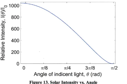
Air mass affects the spectrum and intensity of the light incident on the earth. When light travels along a longer path through the atmosphere, more light is absorbed and scattered by gas and particulate matter in the atmosphere, greatly attenuating the intensity of sunlight incident on the surface of the earth. The solar intensity can be modeled as a function of angle of incident light by the semi-empirical equation:
1(6) = 1.1 1I(0.7AM(y) 0.6 78 ) Cos 6 (11)
where 1 = 1353 W/m2
1000
800-600
400
200 0 0 r/8 7Tr/4 37/8 7r/2Plot of the modeled solar
Angle of indicent light, 0 (rad)
Figure 13. Solar Intensity vs. Angle
intensity versus the angle of the incident sunlight given in equation (11).
Furthermore, the absorption and attenuation of light is not uniform across wavelengths. For example, Rayleigh scattering occurs much more heavily for short wavelength light, causing more blue than red sunlight to be attenuated while passing through the atmosphere. There are a number of scattering and absorption mechanisms such that the attenuation is not linear, but this effect causes significant reddening of the incident spectrum on the Earth's surface for higher air masses.
2.3 Energy Yield
Energy yield is an important metric for understanding solar module performance. Energy yield refers to the total energy harvested by a solar module over a period of sustained time in a specific location and its associated solar spectra. It therefore gives a more complete measure of the performance of a solar panel since it includes the changing solar intensity, spectrum, and angle, giving a realistic prediction of how the device will perform when in the field under real operating conditions.
Energy yield, however, is not the predominant measure of solar device performance. The standardized solar-to-electric conversion efficiency is the most commonly quoted metric for solar
CD
.-panels. The standard testing conditions (STC) for indoor lab efficiency testing under a solar simulator, as determined by the American Society for Testing and Materials, require the tested cell for be at 25*C and be illuminated under a specific spectrum known as AM 1.5 Global (G). This is a carefully determined solar spectrum which replicates the incident spectrum of sunlight on a panel tilted 370 from the normal to the earth's surface in averaged atmospheric conditions for the U.S. [33], under air massl.5. The tilt corresponds to the average tilt needed in the contiguous United States, and this air mass corresponds to when the sun is positioned with a solar zenith angle of
48.190 [33], [34] at sea level, which can correspond, for example, to when the sun is at solar noon
at a location with longitude of +480. The spectrum under this air mass has been shown to be a reasonable average spectrum for the annual solar energy in the United States [33]. STC efficiency is a vital metric for comparing device performance of solar cells, and standardizing device measurements across different labs and organizations.
While STC efficiency does provide important information about a device and how it will perform outside, it is not always an accurate predictor for device performance under practical operating conditions in a range of locations. Energy yield, on the other hand, accounts for all the non-ideal effects of real operating conditions. This can include realistic device temperature, variation in spectrum between locations as well as over the course of each day due to changing air mass, additional absorption and scattering due to humidity and aerosols in the atmosphere, and may include more detailed information about solar conditions such as cloud coverage and other changing environmental factors [11]. Performance under location or time specific spectra and energy yield calculations have been used for the design and analysis of multi-junction concentrator devices, in particular, due to their sensitivity to spectral mismatch [35]-[37]. It has also been shown that optimizing for energy yield, rather than one-sun testing conditions, is a superior method of designing metal grid contacts for single-junction devices [38].
Detailed yield calculations can be carried out using measured spectral, atmospheric data [11], [35] or computational spectral models [36], [37]. However, in this work, air mass and angle of incidence only are considered when performing energy yield, since these are the primary variables which affect metal grid contact loss. Furthermore, because 4T tandems are far less sensitive to spectral variation than 2T tandems and metal contacts have few spectrally sensitive optical properties, the exact variation in spectrum is not considered. Instead, the solar intensity, and thus energy generation, is scaled with air mass with the form of (11).
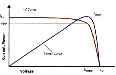
2.3 Current-Voltage Characteristics
Solar cells are diodes, thus they have characteristic exponential current-voltage curves known as I-V curves, like the example shown in Figure 14. The I-V curve of a solar cell under illumination follows the diode equation:
qV
I = IL - I0 (ejik_- 1 ( 12 ) where IL is the photo-generated current, V is the voltage, q is the charge of an electron, k is Boltzmann's constant, T is the temperature, n is the diode ideality factor, and I is the diode leakage current in the dark [32]. A solar cell can operate at any point along this curve, controlled by the applied load resistance. Since power output is the relevant metric, the power needs to be considered when choosing where along this I-V curve a device should be operated. For a solar cell,
qV as voltage increases, the magnitude of the current decreases with the exponential term, I enkT, as shown in equation (12). Since power is the product of voltage and current, there is, thus, a point along this curve where power is at a maximum. This is known as the maximum power point [39]. Another common metric for solar cell performance at maximum power point is Fill Factor (FF). FF is the ratio of the power at maximum power point to the product of the short circuit current (current when V = 0) and open circuit voltage (voltage when I = 0). This gives information about the shape of the I-V curve and the quality of the solar cell.
All solar panels are operated with a maximum power point tracker, so that the device is always operating at the voltage to provide the maximum power [39]. Therefore, it is practical to analyze device performance at the maximum power point since this is the operating point.
I-V Curve Sc max Impp 0 4-0 Power Curve
Voltage Umpp UoC
Figure 14. Solar Cell Current-Voltage, and Power-Voltage Characteristics
An example I-V curve (red) and power vs. voltage curve for a solar cell, illustrating the maximum power point [40].
CHAPTER
3
DEVELOPMENT
4T
CONTACT
Loss
MODEL
The design of metal grid contacts requires optimization to balance series resistance losses and optical shading. We designed a model that analytically computes these losses for a 4T device, and numerically optimizes the metal grid design for a given set of device parameters (Table 1) to minimize total energy yield loss. The details of how our model calculated the power losses due to the shading and resistance losses in the 4T device are described in this section, followed by a brief description of our primary figure of merit, energy yield, and the method of numerical grid optimization.
finger area w x t S2 Top cell, ni t2 Interlayer, n2 .0-W 00
t
3 3 Bottom cell Back metalFigure 15. 4T cross section and variable depiction
Schematic of cross section of 4T tandem device with metal grid finger contacts. All relevant device parameters as described in Table 1 are labeled on this schematic.
Shading and resistance losses are modelled analytically at the maximum-power-point (MPP), using input MPP current densities and voltages before contact loss for the top and bottom cells that can be obtained experimentally or from device simulation. Both current and voltage of each sub-cell in the 4T device are independent, thus the tandem power output per area is the sum of the top and bottom cells' maximum power point outputs,
P = Jmp,tVmp,t + Jmp,b Vmp,b (13)
where Jmp,t and Vmp,t are the MPP current density and voltage, of the top cell and Jmp,b and Vmp,b are the MPP current density and voltage of the bottom cell. The total power per area lost due to shading and resistance of the contacts is then given by:
Pioss = Pideal - Preai = (Jmp,t Iideal 'Vmp,t Iideal + Jmp,b ideal *Vmp,b ideal
( 14)
- (Jmp,t reaea V + Jmp,b real -Vmp,b real)
where Jmp,t ideal' Jmp,bIideal and Vmp,t idea'Vmp,bIideal are the input MPP current densities and
voltages of the top and bottom cell with no losses from contacts. The values ofimp,tI rea'Jmpb Ireal1 and VmptI real, Vmp,b Ireal are the maximum power point current densities and voltages of the top and bottom cell that incorporate shading and resistive losses of the contacts, as computed by the model.
Variable name Description W1, W2, W3 S1, S2, S3 ti t2 P0,1, PO,2, PJ,3 Pfing Jmp,i, Jmp,2 Vmp,1, Vmp,2 L
Effective finger width of (1) top cell front metal grid contact, (2) top cell back metal grid contact, (3) bottom cell front metal grid contact Finger pitch of (1) top cell front metal grid contact, (2) top cell back metal grid contact, (3) bottom cell front metal grid contact
Top cell thickness
Thickness of interlayer between the top and bottom cell
Sheet resistance of the (1) front surface of the top cell, (2) back surface of the top cell, (3) front surface of the front cell
Resistivity of the metal finger material. The reference value is for screen printed silver metal paste.
Current density at maximum power point of (1) the top cell, (2) the bottom cell
Voltage at maximum power point of (1) the top cell, (2) the bottom cell
Length of the fingers of the grid, i.e. the maximum distance current must travel through the finger to reach a bus bar or contact pad
Table 1. Variable definitions
Variable definitions for all necessary device parameters used to model contact yield loss, as shown in the cross-sectional schematic above.
The model calculates contact losses assuming that series resistance only affects device voltage, while shading only affects current [22], [41]. The 'real' current density for each sub-cell when accounting for shading loss is given by:
Jmp,real = Jmp,ideal(1 - fsftade) (15)
where fshade is the fraction of the cell area shaded by metal contacts. The voltage accounting for voltage loss due to contact series resistance is given by:
Vmp,reai = Vmp,ideal - Jmp,real A Reff (16)
where Reff is the effective resistance of the contacts which is calculated analytically, as describe below, and A is the area over which the effective resistance is computed.
3.1 Computing Reff
The series resistance losses of the contacts are calculated analytically from Ohm's law, Pioss = IPReff and is modeled in 2D, neglecting the resistance due to charge traveling vertically
from the bulk of the absorber to the surface. The effective resistance, Reff, is computed assuming uniform current generation and is modelled as described in chapter 2.1.2. The series resistance has two components: the finger resistance, Refffing, and the resistance of the surface between fingers, Reff surf. Thus, from equations ( 4 ) and ( 8) ,the total sheet resistance of any one the
metal grid contact is given by the equation,
1 (pjng L p0 S\
Reff --= A + L
)
(17)12 Afing L
3.2 Computing Shading
Since 4T tandems have stacked contacts, the bottom cell is shaded by its own contacts as well as both the front and back contacts of the top cell. Thus, there are two designs that must be considered: (1) the unaligned case where each set of metal grid fingers is free to have its own finger spacing, and (2) the aligned case when the fingers of different metal grids are aligned. In
the unaligned case, I assume transmission through n grids, Tn, is the product of the probability of light passing through each individual grid,
T = 7JTi =7J (1 - (18)
This approach corresponds to a worst case scenario; however, it is worth noting that, even a slight difference in finger spacing would result in significant misalignment of fingers due to the periodicity of the finger pattern (fingers would align in a beat frequency).
If the fingers are aligned, shading of the bottom cell is reduced since the shadings of the different grids overlap. The amount of overlap, however, is dependent on the angle of incident light since under non-normal incident light, the shading is smeared out and does not all overlap, as depicted in Figure 17. Thus, we consider a varying angle of incident light when considering aligned grid shading. The transmission through a set of aligned grids, Taligned, is given by:
Taligned(0) = 1 - faligned (0) (19)
where faligned (0) is the fraction of area shaded by the aligned grids under light incident at an angle 0 from the normal. This fraction is calculated using Snell's law, to account for bending of light as it passes through different media, and a simple, geometric ray tracing algorithm to calculate the angle dependent shading overlap as a function of angle. The amount that the shading is spread between two stacked contacts depends on the refractive index of the materials between the contacts, n, and the vertical distance between the two contacts, t. These parameters determine how far light can travel laterally as travels from the first to the second contact, d, with the geometric relation,
d = t -tan arcsin -sin
)
(20)((n
Thus, for two subsequent stacked metal grids with finger spacing S, upper grid finger width w, and lower grid finger width w2, and a vertical distance between contacts t1, the shaded fraction is
_
w2
+t1t 1(w
2 -w
1)\faligned(0) = 2 / (21)
S
where 01 = arcsin (sin 0), the angle of light as it transmits through the material between the two stacked contacts with index of refraction nj, from Snell's law. If faligned(0) exceeds Wl W2
S
then it is set to W W2, as this is the physical limit of shading due to two aligned metal fingers.
S
faligned is additionally constrained to a minimum value of zero. A plot of faligned(0 ) for a few
cases is shown in Figure 16.
For all calculations, the ratio of the effective finger width (corresponding to shading), w, to the cross-sectional area of the finger (corresponding to resistance), A, is assumed to be A =
1 w2. This is roughly calculated from the optical and electrical data for 45 pIm screen-printed
3
fingers in [24] to account for total internal reflection of reflected off the metal fingers. While this is an approximation and oversimplifies the optics of a 4T device stack, we do not expect our results to be significantly impacted by this assumption.
2(w/S) C 0 -t/w = 8 t/w = 3 t/w = 1 t/w = 0.1 (w/S) 0 7/8 T/4 3w,/8 i/2
Angle of indicent light,
0
[rad]
Figure 16. Aligned finger shading versus angle
Plot of the shading from two stacked, aligned metal grids each with fingers of thickness, w, and finger spacing, S, versus angle of incident light, given by equation (21).
top cell interlayer bottom cell back metal
I
'7 6 I\
\\
-j (a) (b)Figure 17. Angular dependent shading
Schematic of the cross section of the device, depicting the ray-tracing model and the resulting shade from (a) direct, normal incident light, and (b) oblique light incident at an angle 0 from the normal. The darker areas depict the path of light blocked by the metal fingers and the part
of the sub-cells that is shaded by the metal grid contacts.
3.3 Computing Energy Yield
To account for the angular dependence of the loss due to shading, the model computes the energy yield loss due to the contacts by sweeping over incident angle 0 = [0, 7] to model a full day. To do this we compute the power loss as a function of angle by using the angular dependence of shading given in equations (19) and (21). We use a normalized semi-empirical clear-sky intensity variation from equation (11):
1(0) = (07AM(0)0 6 7 8-1) cos 0 (22)
where AM is the air mass, approximated by equation (10) as AM (0) = , and 1o is the intensity at AM 1.5 and 0 = 0. A plot of the absolute (non-normalized) intensity versus angle of incidence is shown in Figure 13. This equation accounts for both the effect of changing air mass on light intensity and the changing effective area of the device. The current density of each sub-cell is
scaled with this intensity function. Thus, the figure of merit of these contacts is energy yield loss,
Yi0ss, given by:
YIOSS =
f
P10ss(0) d6Jo (23)
= Jmp,ideal 1(0) Vmp,ideal - Jmp,ideal (1 - fshade (0))1()Vmp,real
3.4 Optimization
To find best metal grid geometry for a specific case, we numerically optimize the finger spacings and finger widths to minimize energy yield loss. The top cell front and back metal grid parameters w1, w2, S1, and S2 are first co-optimized to simultaneously minimize (i) yield loss due to shading of the top cell, (ii) resistance loss from the extraction of the top cell current, and (iii) bottom cell current loss due to shading from top cell contacts. Once the top cell contact with the minimum loss is found, the bottom cell contact parameters w3 and S3 are similarly optimized, but with the current density adjusted to account for the shading of the bottom cell by top cell contacts. We expect the impact of the bottom cell grid design on the top cell grid design to be negligible. When any two grids are aligned, the fingers spacings of the aligned grids are constrained to be
equal and the shading is calculated with the corresponding method as described earlier. The metal grid is modelled as a screen printed metal grid with the sheet resistance of silver metal paste. Current large-scale manufacturing screen printing capabilities can reliably produce metal fingers no thinner than around 100 pm, since below this thickness, screen printed fingers may start to be non-uniform and have breaks [24], [42]. Newer technology, however, has shown progress toward thinner fingers as thin as 30 ym [24], [43], so the minimum thickness of mass-production screen printers will likely go down to in the future. To account for this, in this optimization the finger thickness is constrained to be no thinner than 50 pm.
CHAPTER
4
FINGER ALIGNMENT
When designing metal grid contacts for 4T tandems, there are three primary ways the contacts can be integrated: the fingers of all three metal grids can be aligned, the fingers of all three metal grids can be unaligned, or the front and back grid fingers of the top cell can be aligned while the bottom cell fingers are unaligned. While aligning fingers should reduce the total shading to the bottom cell, there may not be a significant reduction in shading to the bottom cell when illuminated by light ofnon-normal incidence. Furthermore, alignment puts an additional constraint on the metal grid design optimization, and thus may increase the impact of other loss mechanism, compared to the unaligned case. Through these analyses, I aim to understand what device parameters make aligning beneficial to energy yield, and how metal grid contacts should be design for 4T tandems.
4.1 Optical Analysis of Finger Alignment
The advantage of aligning metal grid fingers is the potential to reduce bottom cell shading. However, light of non-normal incidence results in the smearing of shade, and less shade overlap. Thus, to explore the shading benefit of alignment, I first examined the optical transmission to the bottom cell though aligned metal grid contacts under a varying angle of incident light. To understand how much light is transmitted through a solar cell with two stacked contacts over a full day when they are aligned, I used equations (19) - (21) to calculate the average shaded area fraction
(w/S) n=1 n=1.5 n=2.5 -n=3.6 (w/S) -0.25 0.5 1 2 4 8 2
t/w
(a) Max. shading Min. shading 0t
n
(b)Figure 18. Average shading two stacked grids versus layer thickness
The average shading due to two identical, aligned stacked metal grids with finger width, w and spacing S, for four incidences of refraction. The minimum possible shading fraction is w (the two
S
grids' shading always entirely overlaps) and the maximum possible shading from is double that, 2 (the two grids' shading never overlaps). A typical t ratio for the top cell (shown in inlet (a))
S w
is around 0.2, and for the interlayer (shown in inlet (b)) is around 10.
2(w/S)
0
m 1.5
<c
![Figure 1. PV Module Price Sensitivity Plot from [2] showing the sensitivity of the minimum sustainable price (MSP) of silicon solar modules to different parameters of module](https://thumb-eu.123doks.com/thumbv2/123doknet/14723290.571037/8.922.100.457.472.714/figure-module-sensitivity-showing-sensitivity-sustainable-different-parameters.webp)