Development of in-situ toughened silicon-rich alloys:
a new class of castable engineering ceramics
by
David S. Fischer
S.M., Materials Science and Engineering Massachusetts Institute of Technology, 2008
B.S., Materials Science and Engineering Lehigh University, 2005
SUBMITTED TO THE DEPARTMENT OF MATERIALS SCIENCE AND ENGINEERING IN PARTIAL FULFILLMENT OF THE REQUIREMENTS FOR THE DEGREE OF
DOCTOR OF PHILOSOPHY IN MATERIALS SCIENCE AND ENGINEERING AT THE
MASSACHUSETTS INSTITUTE OF TECHNOLOGY
September 2010
© 2010 Massachusetts Institute of Technology. All rights reserved.
Signature of Author:_____________________________________________________________ Department of Materials Science and Engineering September 07, 2010
Certified by: ___________________________________________________________________ Christopher A. Schuh Danae and Vasilios Salapatas Associate Professor of Metallurgy Thesis Supervisor
Development of in-situ toughened silicon-rich alloys:
a new class of castable engineering ceramics
by
David S. Fischer
Submitted to the Department of Materials Science and Engineering on September 07, 2010 in Partial Fulfillment of the Requirements for the Degree of Doctor of Philosophy in Materials Science and Engineering
ABSTRACT
Despite having a broad set of desirable properties, silicon’s potential as a primary constituent in a structural material has not yet been realized because of its extremely low fracture toughness. Motivated by the microstructural design techniques used in toughening inherently brittle ceramic materials, this work aims to develop a silicon-rich alloy with microstructural features that provide for the same types of toughening mechanisms displayed by technical ceramics. In order to add true commercial value to these silicon-based alloys, however, the alloys must be processed using methods more flexible and less expensive than the powder processing routes currently used for engineering ceramics. This thesis will discuss the development of a class of castable silicon-based alloys referred to as silicon-disilicide (Si-XSi2) composites, which naturally form a microstructure composed of a silicon matrix and reinforcing disilicide (XSi2) phase during solidification (where X is a transition metal). Experimental work is performed to characterize the thermal, microstructural, and fracture properties of a specific set of Si-(Cr,V)Si2 alloys which are based on the Si-CrSi2-VSi2 system. First, a reliable thermodynamic description of the Si-CrSi2-VSi2 system is obtained, from which the relevant phase diagram is determined. Comparison between simulated solidification paths and experimentally observed microstructures demonstrates the use of the thermodynamic database to predict the phase evolution of the alloys during processing. Long-crack fracture toughness measurements made through chevron-notched beam (CNB) tests show that the toughness of the composite alloys are over 2-3 times that of unalloyed silicon, with in-situ tests revealing the role of microstructural toughening (via crack deflection and crack bridging) on the enhanced fracture properties. Ball-on-disk experiments reveal an order of magnitude improvement in the wear resistance of the alloys compared to silicon. This enhanced short-crack response is linked to the fine microstructural size scale of the eutectic structures, which allow toughening mechanisms to be activated during very early stages of crack growth. The range of fracture toughness and wear resistance values measured for the Si-(Cr,V)Si2 alloys elucidates the potential of these materials as viable structural materials in place of powder-processed ceramics.
Thesis Supervisor: Christopher A. Schuh
Acknowledgements
First, I would like to express my gratitude to the Dow Corning Corporation for funding this work, as well as for their continued support throughout my research program. In particular, I want to thank Dr. Vasgen Shamamian who not only served on my thesis committee, but whose personal commitment to this project has resulted in an amazing collaborative experience with Dow Corning. I would also like to thank the additional members of my thesis committee including Prof. Thomas Eagar and Prof. Ronald Ballinger for all of their guidance and constructive insight. Additionally, I would like to acknowledge Dr. Dimi Katsoulis of Dow Corning and Dr. Fred McGarry of MIT for their participation in many of the early research discussions. There are also many members of the MIT faculty whom I owe much gratitude for their invaluable assistance in the labs throughout this project; most notably of who are Mike Tarkanian, Yinlin Xie, and Don Galler. I want to thank my UROP, Ryan Breneman, for his contributions in the investment casting work. I am also extremely appreciative to have had the opportunity to work alongside all the members who have been part of the Schuh research group. These people have definitely helped make my graduate experience at MIT an enjoyable one. Throughout the years, I have been fortunate enough to have kept an amazing set of friends from back home who I have grown ever closer with from the day I left for school. These people include Dan and Danielle Goikhman, Mike Molé, Rob Messing, Seth Broman, Chris Stout, Ian Zucker, David Munsky, Joe Vitella, Sachin Patel, Eric White, Dana Samet, Marissa Skolnick, Mark Rogers, Meg Cuozzi, and John Morin. While in Boston, I have also becomes friends with a bunch of amazing people including Brian Hohmann, Jay and Lauren Trelewicz, Tim and Allison Rupert, Trey and Jocelyn Holtzwarth, Lindsay Weil, Holly St. Peter, and Charles Snow. It is the company of all my friends that has allowed me to escape the many pressures of graduate school. I want to especially thank my girlfriend, Brooke Viggiano, who has made countless 200+ mile bus rides to be with me over the years and who has always been there when I needed her, even if separated by such a long distance. Of course I am extremely grateful for having such a wonderful family, including all of my uncles, aunts, cousins, and my grandmas Lee Bloom and Dr. Judy Fischer. They have done nothing but supported and encouraged me in all of my endeavors. I want to thank my younger brother, Andrew Fischer, for being an amazing friend – I truly admire the person you have grown to become. There are not enough words that can express my appreciation to my parents, Robert and Alyce Fischer, for everything they have done for me. They have shaped me into the person I am today and there is not one day that goes by that I don’t remember all they have sacrificed so that I may achieve my personal goals – this thesis being the greatest one to date.
Last, but certainly not least, I would like to thank my advisor, Prof. Chris Schuh for his mentorship over the past few years. Chris has challenged me in so many ways and has helped me to accomplish things I never thought possible. He has developed me at both the personal and professional level. His creativity and passion for scientific research is awe-inspiring and I will certainly continue to look up to him in the future.
Table of Contents
Acknowledgements ...3
Table of Contents ...4
List of Figures...7
List of Tables ...21
Chapter 1: How to design an in-situ toughened silicon-rich alloy...24
1.1 Introduction: Silicon as a basis for structural materials... 24
1.2 Fracture properties of silicon and silicon-based materials... 26
1.2.1 Single- and polycrystalline silicon... 26
1.2.2 Structural disilicides... 29
1.2.3 Silicon-rich (eutectic-based) alloys... 34
1.3 Physical, structural, and thermal properties of silicon and disilicides... 36
1.3.1 Physical and structural data ... 36
1.3.2 Thermal expansion data ... 39
1.4 Application of composite design theory to silicon-disilicide eutectic systems ... 41
1.4.1 Toughening in brittle-brittle composites... 41
1.4.2 Achieving microstructural toughening in silicon-based eutectic alloys ... 48
1.5 Problem statement and research objectives ... 62
Chapter 2: Thermodynamic assessment of the Si-rich corner of the Si-Cr-V phase diagram: the Si-CrSi2-VSi2 system...66
2.1 Necessity of Si-CrSi2-VSi2 phase diagram for processing of in-situ toughened Si-(Cr,V)Si2 alloys... 66
2.2 Experimental Procedures ... 66
2.2.1 Differential scanning calorimetry and microstructural analysis ... 66
2.2.2 Computational thermodynamics – the CALPHAD approach... 68
2.3 Experimental Results ... 73
2.3.1 Experimental determination of Si-CrSi2-VSi2 system ... 73
2.3.2 Computational determination of Si-CrSi2-VSi2 system... 83
2.4 Discussion... 87
2.4.2 Calculation of liquidus projections ... 91
2.5 Concluding Remarks... 93
Chapter 3: Microstructural effects on the long-crack behavior of in-situ toughened Si-(Cr,V)Si2 alloys...94
3.1 Alloy and process design ... 94
3.1.1 Role of alloy composition on microstructural toughening in eutectic Si-(Cr,V)Si2 alloys... 94
3.1.2 Role of processing on the microstructural evolution of die cast Si-(Cr,V)Si2 alloys and the ensuing fracture properties... 94
3.2 Experimental Procedures ... 95 3.2.1 Alloy preparation ... 95 3.2.2 Mechanical Testing... 96 3.2.3 Microstructural characterization ... 100 3.3 Experimental Results ... 101 3.3.1 Microstructural analysis... 101
3.3.2 Chevron-notched beam fracture tests... 107
3.4 Discussion... 121
3.4.1 Considerations of alloy and process design on the isotropy of the fracture toughness of in-situ toughened Si-(Cr,V)Si2 alloys processed using multidirectional solidification ... 121
3.4.2 Effect of overgrowth during anomalous eutectic solidification on the observed long-crack fracture toughness of in-situ toughened Si-(Cr,V)Si2 alloys... 124
3.5 Concluding Remarks... 126
Chapter 4: Effects of microstructural toughening on the sliding wear resistance of in-situ toughened Si-(Cr,V)Si2 alloys ...128
4.1 Role of microstructural toughening on wear response of Si-(Cr,V)Si2 alloys ... 128
4.2 Experimental Procedures ... 129 4.2.1 Alloy preparation ... 129 4.2.2 Wear Testing... 130 4.2.3 . Hardness Testing... 131 4.3 Experimental Results ... 132 4.3.1 Microstructural analysis... 132
4.3.2 Wear tests... 134
4.3.3 Hardness Measurements ... 139
4.4 Discussion... 140
4.4.1 Effects of microstructural toughening on the wear response of Si-(Cr,V)Si2 alloys during sliding wear ... 140
4.4.2 Lateral fracture model with R-curve effects ... 146
4.4.3 Testing for grain size effects on wear in silicon ... 152
4.5 Concluding Remarks... 153
Conclusions...155
Directions for future work ...161
Appendix A: Design of DSC experiments...166
Appendix B: Thermodynamic parameters of the Si-Cr-V system and experimental thermodynamic data for selected alloys...168
List of Figures
Figure 1.1: Ashby plot of specific fracture toughness (KIc/ρ) versus specific strength (σf/ρ). Silicon’s high strength and low density make its specific strength one of the highest compared to those displayed by engineering ceramics. However, silicon’s extremely low fracture toughness make its specific toughness only half of that displayed by most engineering ceramics.
Figure 1.2: Temperature dependence of the critically resolved shear stress (CRSS) for primary slip on systems (noted in legend) which are accessible at low temperatures in various disilicide single crystals (as measured in compression). All structures show a negative temperature dependence in their CRSS with some anomalous strengthening at elevated temperatures (except CrSi2 which shows no strengthening). Slip in MoSi2 single crystals requires a noticeably higher CRSS at room temperatures than do other disilicides. Also, no slip is observable in CrSi2 for which failure without plastic flow has been observed to occur at 718 MPa at around 700 °C (open blue diamond). (Data compiled from the following sources: MoSi2 [45] (open circle is interpolated from data); NbSi2, TaSi2 [45]; CrSi2 [45] and [60]; VSi2 [59]; TiSi2 [65]; CoSi2 [66])
Figure 1.3: Vickers indent (1000 gf load) in a MoSi2 (C11b) / NbSi2 (C40) duplex silicide showing crack arrest at the lamellar interface. (Image reproduced from [70])
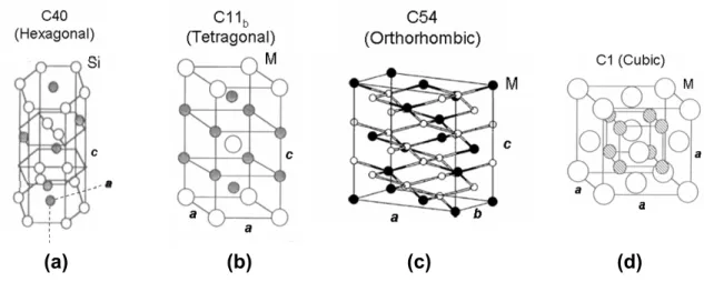
Figure 1.4: Hard-sphere models of crystal structures for common structural disilicides. Identification of the atom type in each structure is shown at the top right atom and is designated as either M (transition metal) or Si (silicon). (Images (a), (b), and (d) reproduced from [47] and (c) reproduced from [85])
Figure 1.5: (a) Atomic arrangement of transition metal layers (MSi2) found in many structural disilicides. These layers correspond to the (110), (0001), and (001) planes for C11b, C40, and C54 structures, respectively. (b) Stacking sequence of atoms on close packed planes according the transition metal layer sites shown in (a). (Images reproduced from [68])
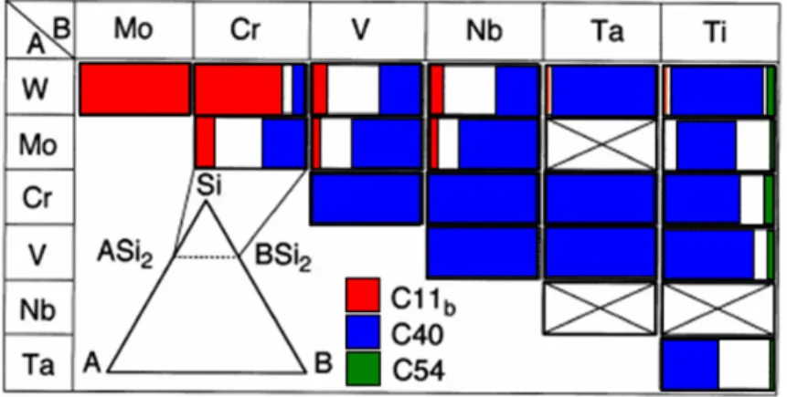
Figure 1.6: Schematic of ASi2-BSi2 pseudo-binary diagrams between different transition metals disilicides (where A and B represent the different transition metals listed in this table). Compositional regions of stability for the single disilicide structures are shown by different markings, whereas regions of two-phase equilibrium (i.e. no single stable phase) are shown by the white regions. (Image adapted from [81] which is based on data published in [78])
Figure 1.7: Effect of volume fraction and reinforcing particle shape on the degree of toughening achieved by the crack deflection mechanism. (a) The relative crack resistance force of the composite (GC) compared to the matrix (GM) is increased for increasing volume fractions of second phase particles. Also, for a given volume fraction of particles, the effectiveness of toughening is greatest for rod shaped (elongated) particles and least for sphere shaped. (b) Increasing the aspect ratio of elongated particles, such as rods, leads to an increase in the relative toughening achieved by crack deflection. (Images reproduced from [91] which is based on data published in [88])
Figure 1.8: (a) The crack opening displacement of a material reinforced with a discontinuous elastic second phase is controlled by the elastic properties of the reinforcement as well as the interfacial properties between the matrix and reinforcing phase. (b) Bridging traction (T) versus distance behind the crack tip (x) for reinforcement with a discontinuous elastic (brittle) ligament experiencing no interfacial friction with matrix. (Image (a) and inset image in (b) reproduced from [102])
Figure 1.9: R-curve behavior for alumina matrix composites reinforced with various volume fractions of silicon carbide (SiC) whiskers. The rising slope of the R-curve and the final (steady state) fracture toughness of the composites increase as the volume fraction of SiC reinforcements increase. This is due to an increase in the bridging zone size, and thus, a larger contribution to crack opening displacement by the fiber reinforcements. (Image reproduced from [94])
Figure 1.10: Periodic table highlighting the different types of binary Si-X eutectic reactions that occur in the Si-rich region of the respective phase diagrams, where X is the alloying element.
The red elements do not form any eutectics in the Si-rich region of the Si-X binary phase diagram, whereas the blue and green elements (transition metals) all form silicide-silicon eutectics in the Si-rich region of the Si-X binary phase diagram.
Figure 1.11: (a) The binary phase diagram for the Si-Al system is an example of a Si-X system in which a single Si-poor eutectic occurs over the entire composition range (in this case at 12.6 wt. % Si). During solidification of an alloy with a Si-rich composition, solidification through the primary Si region results in the formation of large primary silicon grains which degrade the fracture properties of the alloy, as shown in (b) for a Si-42Al (wt. %) alloy. (c) The binary phase diagram for the Si-Ti system is an example of a Si-X system in which a eutectic reaction occurs in the Si-rich region of the phase diagram (in this case at ~ 75 wt. % Si) to form a silicon-silicide fully eutectic microstructure, as shown in (d) for Si-TiSi2. Microstructural toughening is expected to occur in such a material due to the absence of large silicon grains and the homogenous distribution of the reinforcing phase (TiSi2) which maximizes the amount of crack-reinforcement interactions. (Phase diagrams reproduced from [111] which are based on data from [109] and [112] for the Si-Al and Si-Ti systems, respectively. Micrograph (b) was reproduced from [5] and (d) from [105]).
Figure 2.1: Schematic of the DSC experimental approach used to identify the eutectic alloy compositions within the Si-CrSi2-VSi2 ternary phase field. First, the Si-VSi2 (e1) and Si-CrSi2 (e2) binary eutectic compositions were identified. Afterwards, alloy compositions along Si isopleths which traversed the two binary eutectic points were studied. Eutectic compositions were identified by those that displayed a single melting peak and contained a eutectic microstructure (as determined by microstructural analysis of the tested DSC specimen).
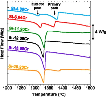
Figure 2.2: A set of DSC curves for alloy compositions along the binary Si-CrSi2 line reveals a change in the number of endothermic peaks measured as the alloy passes through the eutectic composition. Alloys containing a relatively high degree of primary Si (Si-4.00Cr, Si-6.04Cr) or CrSi2 (Si-20.20Cr) have a distinguishable second peak. Such DSC data was used to select possible eutectic compositions (i.e. single-peaked curves) for further microstructural analysis and
final identification of the eutectic alloy (Si-12.09Cr in this case). A similar analysis was performed for the Si-VSi2 binary system. (All compositions are given in at. %).
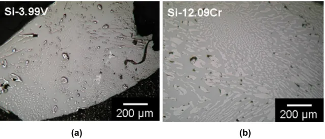
Figure 2.3: Micrographs of the binary (a) Si-3.99V and (b) Si-12.09Cr alloys that were selected as the Si-VSi2 and Si-CrSi2 eutectic compositions, respectively. Both alloys displayed (near) fully-eutectic structures containing no primary or overgrown silicon or disilicide phase regions. The eutectic structures were (a) fibrous and (b) colony type. In these micrographs, the darker regions are the Si phase and the brighter regions are the respective VSi2 and CrSi2 phases.
Figure 2.4: DSC curves for alloy compositions along the CrSi2-VSi2 binary line show a clear shift in the disilicide peak position to higher temperatures as the V content is increased. This suggests that the melting point of the (Cr,V)Si2 phase monotonically increases along the binary line from CrSi2 to VSi2. However, the multiple peaks in the DSC signals indicates that these disilicide compounds are not free of secondary phases and thus caution should be made in acceptance of the absolute melting temperatures as measured from these peaks – especially at higher V contents where peak broadening is observed to occur to due large variations in the alloy compositions.
Figure 2.5: Diagram showing the alloy compositions along six isoplethic sections that were experimentally investigated (by combined DSC and microstructural analysis) to determine the eutectic boundary curve between the binary Si-VSi2 (e1) and Si-CrSi2 (e2) eutectic points found in Part I of this section.
Figure 2.6: DSC curves for alloy compositions along the 88.85 at. % Si isopleth (isopleth 6 in Fig. 2.5) display sharp eutectic peaks corresponding to melting along the eutectic boundary curve. The primary peaks for alloy compositions in the ternary phase field are less distinct than for binary compositions (Fig. 2.4) due to the variability of the (Cr,V)Si2 composition (i.e. changes in the Cr:V ratio) as opposed to the constant binary CrSi2 or VSi2 compositions demanded by stoichiometry.
Figure 2.7: Magnified view of the primary (Cr,V)Si2 peaks identified in Fig. 2.6. As the degree of primary (Cr,V)Si2 solidification is increased [from alloy (f)-(a)], the primary peaks become more removed from the initial eutectic peak since the liquidus temperature of the alloy increases.
Figure 2.8: Series of micrographs for alloy compositions 3b – 3d (92.62 at. % Si isopleth) showing a transition from (a) primary (Cr,V)Si2 solidification to (b) eutectic solidification to (c) primary Si solidification as the compositions traverses the ternary eutectic curve.
Figure 2.9: Micrographs of the alloy compositions that were experimentally determined to lie along the eutectic boundary curve within the Si-CrSi2-VSi2 ternary system. A eutectic point was identified for each of the 6 isopleths in Fig. 2.5.
Figure 2.10: Calculated binary phase diagrams for the (a) Si-Cr and (b) Si-V systems based on the optimizations in [144] and [143], respectively. The computed eutectic and melting reactions in the Si-MSi2 region of both diagrams agree closely with those experimentally determined in Section 2.3.1 Part I.
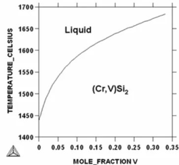
Figure 2.11: Calculated liquidus temperature of (Cr,V)Si2 as a function of the vanadium content. The liquidus temperature of (Cr,V)Si2 in shown in consistently increase from 1439 °C (for CrSi2) to 1677 °C (for VSi2) as vanadium is substituted for chromium.
Figure 2.12: The calculated eutectic boundary curve (red line) is plotted with the experimentally investigated alloy compositions (the blue triangles denoting the compositions identified as eutectic boundary points in Section 2.3.1 Part III). Excellent agreement between the calculated and experimental eutectic curves demonstrates the self-consistency of the thermodynamic parameters used to describe the Si-CrSi2-VSi2 system.
Figure 2.13: The alloy compositions used in the fracture (Ch. 3) and wear (Ch. 4) studies are plotted with the experimental and calculated eutectic points determined for the Si-CrSi2-VSi2 system. Equilibrium solidification paths were simulated for each of these compositions so that they could be compared with actual microstructures observed for cast Si-(Cr,V)Si2 alloys.
Figure 2.14: Simulated equilibrium solidification paths for four of the Si-(Cr,V)Si2 alloys that were experimentally investigated in Chapter 3 and 4. Binary alloys (a) A and (b) D undergo a large degree of primary solidification prior to reaching the invariant eutectic reaction. Ternary alloys (c) C and (d) G undergo univariant eutectic solidification after some degree of primary (Cr,V)Si2 and Si solidification, respectively. (See Fig. 2.13 for alloy letter designations).
Figure 2.15: Isothermal lines (solid colored lines) calculated for the Si-CrSi2-VSi2 system in the region near the eutectic boundary curve. The colored shading in the experimental data points indicates the temperature range within which the melting point was measured. Satisfactory agreement between the measured melting points and the calculated liquidus curves is indicated by the tendency of the measured melting temperatures to fall between the corresponding colored liquidus lines for that temperature range. This agreement is another good indicator of the self-consistency of the thermodynamic parameters used to describe the Si-CrSi2-VSi2 system.
Figure 3.1: Schematic of chevron notch dimensions used for the CNB specimens.
Figure 3.2: Different orientations used for machining of CNB specimens. For the alloy D CNB specimens machined from the sides of the casting, the notches in orientations 1 and 2 were machined perpendicular to one of the preferred disilicide growth directions, whereas notches in orientation 3 were machined parallel to both of the preferred growth directions.
Figure 3.3: Chevron-notched four-point bend test fixtures used for the (a) Instron test method and (b) in-situ test method with an SEM. The fixture in (a) was used to obtain high resolution force vs. displacement data, while the fixture in (b) was used to image crack propagation during CNB testing.
Figure 3.4: (a) Back-scatted electron images of the Si-(Cr,V)Si2 alloys (alloy D shown here as an example) were used to create (b) segmentation images to determine the volume fraction of the individual phases composing the microstructure. The silicon phase is colored in green and the disilicide phase is colored in blue.
Figure 3.5: Alloy A (Vf = 6.7%) is shown to have a fibrous microstructure with some unbranched plates. The SEM micrograph in (b) is a magnified view of the microstructure shown in (a). (SEM images were taken using back-scattered imaging)
Figure 3.6: Alloy B (Vf = 19.9 %) has an irregular structure composed of massive branched and unbranched plates. The SEM micrograph in (b) is a magnified view of the microstructure shown in (a). (SEM images were taken using back-scattered imaging)
Figure 3.7: Alloy C (Vf = 23.8%) has a mostly an irregular branched-plate structure with some complex regular structure. The SEM micrograph in (b) is a magnified view of the microstructure shown in (a). (SEM images were taken using back-scattered imaging)
Figure 3.8: Alloy D (Vf = 39.6 %) specimens machined from the center of the casting display quasi-regular growth which consists of a pseudo-colony type structure with high alignment of the disilicide phases about a specific growth direction. The SEM micrograph in (b) is a magnified view of the microstructure shown in (a). (SEM images were taken using back-scattered imaging)
Figure 3.9: Alloy D (Vf = 31.3%) specimens machined from the sides of the casting display the same colony type structure as the specimens machined from the center of the same casting (Fig. 3.8). Overgrowth of the silicon phase has occurred in this region of the casting due to the more rapid solidification rates near the mold walls from where these specimens were machined. With respect to Fig. 3.2 , the micrographs were taken from notch planes of orientation (a,b) type 1, (c,d) type 2, and (e,f) type 3 (where (b), (d), and (f) and are magnified views of the microstructures shown in (a), (c), and (e), respectively). A higher fraction of the disilicide lamellae grew in a direction nearly perpendicular to the notches cut in orientations 1 and 2 than those cut in orientations 3. (SEM images were taken using back-scattered imaging)
Figure 3.10: (a) Sudden load drops from the initial linear portion of the load-extension curves for unalloyed silicon CNB test specimens indicate unstable fracture due to overload, and thus invalid test data. (b) Fracture ridges extending from the chevron tip and (c) tortuous crack paths were observed in transverse and longitudinal fractographic images of the silicon notch planes,
respectively. These images suggest extremely unstable crack initiation and propagation which is in agreement with the load-extension response of this material. (SEM images in (b) and (c) were taken using secondary and back-scattered imaging, respectively)
Figure 3.11: (a) Load-extension curves for Hexoloy® SA silicon carbide CNB specimens revealed pop-in followed by a subsequent load increase (stable fracture) to the maximum load at which point catastrophic failure occurred. A well-behaved fracture pattern in this material was noted by (b) flat, smooth fracture surfaces in transverse fractographic images of the notch plane, as well as by (c) straight crack propagation paths in longitudinal fractographic images of the notch plane. Such fracture behavior is characteristic of a material that displays single-value toughness (i..e flat R-curve) and that fails in an catastrophic manner (as noted in the load-extension response). (SEM images in (b) and (c) were taken using secondary and back-scattered imaging, respectively)
Figure 3.12: (a) Load-extension curves for Si-(Cr,V)Si2 CNB specimens revealed an initial pop-in followed by a load pop-increase (stable crack propagation) with a smooth transition through the maximum load. (b) Transverse images of the crack planes of the Si-(Cr,V)Si2 composites show a rough fracture surface with delamination between the Si and (Cr,V)Si2 phases. (c) Longitudinal images of the crack planes after unloading of the CNB specimens once the maximum load was reached (but before complete fracture) demonstrates that fracture was controlled through crack deflection and bridging mechanisms. Both fractographic images support the predictions of weak interfaces between the silicon and disilicide phases due to residual tensile stresses as discussed in Chapter 1 (Section 1.4.2 Part II-C). Such fracture behavior is characteristic of a material that displays a rising R-curve and that fails in a non-catastrophic manner (as noted by the gradually decreasing portion of the load-extension curve). (SEM images in (b) and (c) were taken using back-scattered imaging)
Figure 3.13: Two types of fracture responses observed during CNB testing of alloy D specimens machined from the center of the casting. (a) When the (Cr,V)Si2 reinforcements near the notch walls were oriented parallel to the crack direction, fracture would occur only along those walls, away from the center of the notch. (b) When the (Cr,V)Si2 reinforcements were oriented
perpendicular to the crack direction, extensive crack deflection and bridging forced the crack completely out of the notch region. (SEM images were taken using back-scattered imaging)
Figure 3.14: Large silicon regions around the notch tips of alloy D CNB specimens machined from the sides of the casting provided low resistance paths of crack propagation to occur within the notch plane. This allowed for valid fracture toughness data to be obtained for these specimens. Shown here is a specimen machined with a notch orientation of type 1 (see Fig. 3.2). (SEM image was taken using back-scattered imaging)
Figure 3.15: Transverse images of the notch regions for the CNB specimens that displayed (a-c) the highest and (d-f) the lowest fracture toughness values in the ranges cited for the various alloys (Table 3.4). In all of the notch regions of specimens displaying the maximum toughness value, a fully or near-fully eutectic structure is observed around the notch tip. On the other hand, large Si regions existed in the notch tip region for those specimens displaying minimum toughness values. (SEM images were taken using back-scattered imaging)
Figure 3.16: Collage of micrographs taken during the in-situ testing of alloy B. The column of micrographs on the right correspond to those taken from region A, those in the middle to region B, and those on the right to region C. (SEM images taken using back-scattered imaging)
Figure 3.17: (a) Back-scattered electron micrograph of a fully eutectic alloy D specimen at the point of final fracture during in-situ CNB testing. (b) Magnified view of the chevron-notch tip region marked in (a) (by red rectangle) shows that nearly all of the disilicide reinforcements are aligned parallel to the direction of crack propagation, resulting in minimal initiation of the deflection and bridging toughening mechanism.
Figure 3.18: Load-crack extension curve for alloy B based on in-situ CNB test measurements (Fig. 3.16) were used to estimate the fracture toughness of a fully eutectic alloy D specimen (Fig. 3.13b) in which the disilicide reinforcements within the eutectic colonies are oriented perpendicular to the crack propagation direction. The data point marked by the black square is the load and crack extension at which the crack was observed to leave the notch plane in Fig.
3.13b. The load-crack extension data was fitted using a linear function in the regime governed solely by the material’s R-curve behavior (i.e. where the stress intensity function for the chevron-notch geometry produces an increasing elastic strain energy release rate, or more simply, unstable fracture).
Figure 3.19: Schematic of a eutectic colony microstructure which exhibits a random distribution of the reinforcing minor phase orientation as marked by the bold lines or circles (circles represent an orientation into the plane of the page). As a crack propagates through a region low crack resistance region (where the colony is oriented parallel to the crack direction), it is likely to encounter regions of high crack resistance (where the colonies are oriented more perpendicular to the crack direction) before finding another low crack resistance path. This type of microstructure is expected to enhance the isotropy of in-situ toughened Si-(Cr,V)Si2 alloys by ensuring that microstructural toughening mechanisms, such as crack bridging, are activated prior to excessive crack growth.
Figure 3.20: Illustration showing how postponement of the rising R-curve behavior in Si-(Cr,V)Si2 alloys leads to reduced fracture toughness values (KIvb) as measured by the CNB method. In this example, the delayed rising R-curve response of alloy X2 compared to an alloy X1 of the same composition is due to the presence of overgrown silicon regions near the notch tip which provide low energy fracture paths. This type of effect is expected to greatly reduce the reliability of Si-(Cr,V)Si2 composites.
Figure 4.1: Ball-on-disk test apparatus used for wear testing of Si and Si-(Cr,V)Si2 composites. (Image reproduced from http://www.csm-instruments.com/en/Tribometer)
Figure 4.2: (a) As-cast unalloyed silicon displays a coarse microstructure consisting of large (102-103 μm) grains. Ternary (b) alloy E (Vf = 14.9 %), (c) alloy F (Vf = 20.8 %), and (d) alloy G (Vf = 27.4 %) display a mixed irregular and complex regular structure. Binary (e) alloy H [magnified in (f)] displays a colony structure. (Silicon etched with 200 mL distilled H2O and 100 g NaOH. SEM images taken using secondary imaging at an accelerating voltage of 20 kV)
Figure 4.3: Wear track profiles measured for unalloyed Si and alloy H after testing at three different normal loads. At 1 N, both (a) silicon and (b) alloy H display very mild wear indicative of a microfracture wear mechansism. At 3 N, (c) silicon starts to undergo severe wear caused by macrofracture events, whereas (d) alloy H still displays a low wear rate due to enhanced toughening in the composite. At 6 N, both (e) Si and (f) alloy H undergo severe wear.
Figure 4.4: The shapes of the coefficient of friction (μ) curves during sliding wear can be identified with an underlying mode of wear for the given testing conditions. (a) At W = 1 N, very smooth curves and high values of μ indicate that adhesive wear mechanisms (characteristic of mild wear) are active at low loads. (b) At W = 3 N, the Si-(Cr,V)Si2 alloys display the same smooth curves as in (a) indicating they are still within the mild wear regime. However, the ‘noisy’, undulating curve displayed for Si at this load indicates successive fracturing (peaks) / material removal (valleys) events are taking place. (c) At W = 6N, silicon and two of the composite alloys (alloy E and F) are shown to display undulating μ-curves, whereas alloys G and H maintain smooth curves suggesting that large-scale material removal is minimal for the latter two alloys.
Figure 4.5: Comparison of the wear rate constant (right-hand term of Eq. 4.3) for Si and the Si-(Cr,V)Si2 alloys within fracture-dominated wear regimes (W ≥ 2 N) show that the alloys display wear rate constants (which are inversely proportional to wear resistance) an order of magnitude lower than unalloyed Si. The region highlighted in blue signifies the typical range of wear rate constants displayed by technical engineering ceramics commonly used as tribological components.
Figure 4.6: Illustration depicting the crack system formed underneath a sharp asperity during sliding wear. Lateral cracks that form underneath the surface and propagate perpendicular to the sliding direction can reach the surface of the material, causing extensive material removal (highlighted in red). (Image was adapted from [169])
Figure 4.7: Plot of the wear rate versus applied load during sliding wear of Si and Si-(Cr,V)Si2 alloys shows a transition from mild to severe wear as indicated by an increase in the slope of the
data. The critical load necessary to induce this transition was found to be lower for Si (Wc = 1 N) than for the alloys (Wc = 4 N).
Figure 4.8: Linear correlation between the wear rates and mechanical property factors (from Eq. 4.4) for Si and Si-(Cr,V)Si2 alloys indicates the lateral fracture model is appropriate for describing the material removal process within the severe wear regime for the given set of testing conditions.
Figure 4.9: SEM analysis of the wear tracks of test specimens taken after testing at a load of 6 N reveal the effects of microstructural toughening on the wear response of these materials. (a) Deep asperity grooves and large wear debris show ease of lateral crack propagation in Si. (b) Crack bridging within the eutectic regions of alloy F is shown to prevent large Si fragments from becoming removed from the specimen surface. (c) No large wear fragments are shown to have formed in alloy H due to the lack of overgrown Si regions. Instead, a thin tribolayer consisting of small, compacted wear particles is present on the surface of the specimen. (d) Illustration showing the orientation relationship between the sliding direction, lateral crack planes, and eutectic colonies of alloy H shown in (c). (SEM images taken using (a) secondary and (b), (c) back-scattered imaging at an accelerating voltage of 20 kV)
Figure 4.10: Effects of microstructural toughening on the formation of lateral cracks due to asperity sliding contact is modeled by Vickers indentation at various loads. At a low load of W = 1N, the extent of lateral fracture is not large enough to activate toughening mechanisms such as crack bridging – thus causing (a) unalloyed Si and Si-(Cr,V)Si2 composites such as (b) alloy H to display the same wear behavior. At a higher load of W = 3 N, lateral fracture is large enough to activate toughening mechanisms in the Si-(Cr,V)Si2 composites, resulting in much more extensive material removal in (c) Si than compared to composites such as (d) alloy H. This helps to explain the large difference in wear rates measured for the materials at high loads (Fig. 4.7)
Figure 4.11: Calculated R-curve for Si-(Cr,V)Si2 alloys as a function of the limiting lateral crack size as implicitly solved through Eq. 4.5b. An arctan R-curve relation [170] was used for this
derivation, with the listed parameters being estimated values based on experimental observations.
Figure 4.12: Critical load necessary to induce lateral fracture as a function of the applied load. For the Si-(Cr,V)Si2 alloys, the critical load increases with applied load due to their increasing toughness with lateral crack size (see Fig. 4.11). This is in contrast to Si for which the critical load is a constant due to its flat R-curve behavior. As a result, the threshold for lateral fracture (W*), where W > Wc, is much higher for the Si-(Cr,V)Si2 composites than for Si.
Figure 4.13: Calculated and experimental wear rates for Si and Si-(Cr,V)Si2 alloys. By incorporating an R-curve relation for the fracture toughness of the Si-(Cr,V)Si2 alloys, the lateral fracture model is able to account for the microstructural toughening effects on fracture-induced wear and accurately predict the wear behavior of both flat and rising R-curve materials.
Figure 4.14: Microstructure of a fine-grained polycrystalline Si specimen (dg ≈ 1 – 10 μm) for which wear testing was performed at 3 N using the same experimental procedure as described in Section 4.2.2. The wear rate measured for this specimen was the same as the coarse-grained Si specimen (Fig. 4.2a) tested at the same load – indicating the microstructural independence of the wear response of unalloyed Si. The absence of a grain-size effect on the wear behavior of silicon agrees with previous studies which show that the fracture toughness of Si is independent of its microstructure. (Silicon etched with 200 mL distilled H2O and 100 g NaOH)
Figure 5.1: Ashby plot of specific fracture toughness (KIc/ρ) versus specific strength (σf/ρ). By more than doubling or tripling silicon’s fracture toughness without greatly increasing its density, in-situ toughened Si-(Cr,V)Si2 composites can achieve specific strength and toughness values within the same range as those displayed by most engineering ceramics.
Figure 5.2: Ashby plot of the dry wear rate constant (i.e. wear rate) versus hardness. An order of magnitude improvement in the wear rate constant of the Si-(Cr,V)Si2 alloys (~ 10-14 m2/N) over the unalloyed Si matrix (~ 10-13 m2/N) puts the wear properties of this new class of alloys in the same regime as those displayed by some engineering ceramics, cermets, and nitrided steels –
all of which are used as tribological components in applications where abrasive wear is a concern. It should be noted that the wear rate constants shown in the plot are given for operating pressures that are a fraction of the maximum bearing pressure (P/Pmax) for a given material such that ka is a true constant (i.e. does not increase with increasing load). The maximum bearing pressure is proportional to the hardness of the material. (Image adapted from [171])
Figure 6.1: (a) During solidification of a Si-CrSi2 alloy with Ag additions [Si-17.7Cr-6.7Ag (wt.%)], Ag forms a low melting eutectic with Si that solidifies within the Si-CrSi2 eutectic structure or at the eutectic boundaries. (b) During solidification of a Si-CrSi2 alloy with Sn additions [Si-17.6Cr-7.3Sn (wt.%)], Sn is rejected from Si and CrSi2 crystals that grow during Si-CrSi2 eutectic growth and solidifies at the boundaries of the Si-CrSi2 eutectic colonies. At the eutectic boundaries, the Sn phase will provide ductile phase toughening mechanisms such as crack arrest as shown in (c) during Vickers indentation (100 g) performed on the alloy.
Figure 6.2: Photograph of an MIT medallion that was produced through an investment casting process with a Si-20.29Cr (wt.%) alloys. The intricate details captured in the medallion demonstrates the advantage of the castable Si-rich alloys over powder-processed ceramics of being able to be easily processed into complicated geometries. The dimensions of the medallions were diameter = 6 cm and thickness = 0.6 cm.
Figure A.1: DSC thermal signal measured during the isothermal melting stage (T = 1600 °C) for a Si-13Cr (at. %) alloy. The curve levels off after about 30 min indicating that melting of the raw materials is completed.
Figure A.2: DSC curve for a pure silicon specimen that was processed and analyzed using the same experimental procedure as for the Si-(Cr,V)Si2 alloys (see Section 2.2.1). The melting temperature (Tm) and enthalpy of melting (ΔHm) measured for silicon (shown on graph) agreed extremely well with those reported in literature, thereby demonstrating the minimal extent to which the silicon was contaminated by reaction with the Al2O3 sample pan during melting.
List of Tables
Table 1.1: Fracture toughness values measured for various forms of single crystalline silicon
Table 1.2: Fracture toughness values measured for various polysilicon microstructures
Table 1.3: Physical and structural data of silicon and some common structural disilicides
Table 1.4: Linear and volumetric thermal expansion coefficients for silicon and structural disilicides
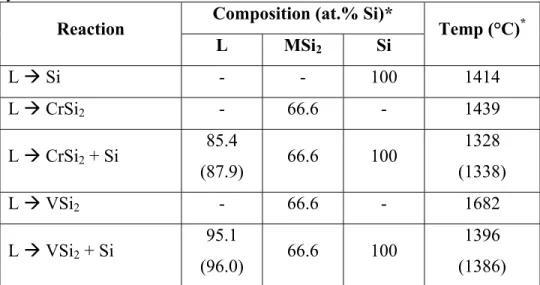
Table 1.5: Data for silicon-disilicide eutectic reactions (compositions and temperatures from [113])
Table 1.6: Young’s modulus of disilicides (EMSi2) and their respective Si-MSi2 eutectic alloys
(E )c
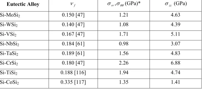
Table 1.7: Estimated circumferential (σrr,σθθ) and longitudinal σzz stresses on a MSi2 fiber in an infinite matrix of Si
Table 2.1: Melting and eutectic reactions in the binary Si-CrSi2 and Si-VSi2 systems
Table 2.2: Calculated fractions of primary solidification and disilicide content for experimentally investigated Si-(Cr,V)Si2 alloys in Chapter 3 (alloys A-D) and Chapter 4 (alloys E-H)
Table 3.1: Si-(Cr,V)Si2 alloy designations and compositions used in all experiments described in Chapter 3
Table 3.2: Dimensions of graphite molds used to cast Si-(Cr,V)Si2 alloys for experiments in Chapter 3
Table 3.3: Experimental versus calculated disilicide volume fractions
Table 3.4: Experimentally measured chevron-notched beam fracture toughness (KIvb) values
Table 3.5: Disilicide spacing in the notch regions of CNB specimens
Table 3.6: Load-crack extension measurements made on Si-(Cr,V)Si2 CNB specimens during in-situ testing.
Table 4.1: Alloy compositions used for sliding wear analysis
Table 4.2: Dimenions of graphite molds used to cast alloys for wear experiments
Table 4.3: Experimental versus calculated disilicide volume fractions
Table 4.4: Vickers hardness for Si, CrSi2, VSi2 and Si-(Cr,V)Si2 alloys
Table 4.5: KR as a function of load and lateral crack length for Si-(Cr,V)Si2 alloys
Table B.1: Summary of thermodynamic parameters in the Si-Cr-V system*
Table B.2: Enthalpies of melting (ΔHm) and liquidus temperatures (Tm) for alloys in the binary Si-CrSi2 system (bold composition was determined to be eutectic)
Table B.3: Enthalpies of melting (ΔHm) and liquidus temperatures (Tm) for alloys in the binary Si-VSi2 system (bold composition was determined to be eutectic)
Table B.4: Enthalpies of melting (ΔHm) and liquidus temperatures (Tm) for alloys in isopleth 1 (95.46 at. % Si) system (bold composition was determined to be eutectic)
Table B.5: Enthalpies of melting (ΔHm) and liquidus temperatures (Tm) for alloys in isopleth 2 (94.51 at. % Si) system (bold composition was determined to be eutectic)
Table B.6: Enthalpies of melting (ΔHm) and liquidus temperatures (Tm) for alloys in isopleth 3 (92.62 at. % Si) system (bold composition was determined to be eutectic)
Table B.7: Enthalpies of melting (ΔHm) and liquidus temperatures (Tm) for alloys in isopleth 4 (91.68 at. % Si) system (bold composition was determined to be eutectic)
Table B.8: Enthalpies of melting (ΔHm) and liquidus temperatures (Tm) for alloys in isopleth 5 (89.80 at. % Si) system (bold composition was determined to be eutectic)
Table B.9: Enthalpies of melting (ΔHm) and liquidus temperatures (Tm) for alloys in isopleth 6 (88.85 at. % Si) system (bold composition was determined to be eutectic)
Chapter 1: How to design an in-situ toughened silicon-rich alloy
1.1 Introduction: Silicon as a basis for structural materials
Being that silicon is the second most abundant element on earth, making up about 25.7% of the earth’s crust [1], it is no surprise that this material has been so extensively studied for a wide variety of applications. In microelectronic devices, as a popular alloying element in aluminum alloys and steels, or even as a constituent in polymeric silicone compounds, silicon has been the major focus of research in a large number of engineering fields and industries. Through such research the properties of silicon have been thoroughly characterized [2-4]. A majority of the properties studied, however, pertain to silicon in its single crystalline form. This is especially true for the mechanical properties, or more specifically, the fracture characteristics of silicon.
It is widely known that at relatively low temperatures (below about half of its melting temperature) silicon is an inherently brittle material due to the nature of its covalent bonding and diamond cubic crystal structure. Perhaps it is for this reason that manufacturers of silicon have rarely considered the possibility of using this material as a major component in structural engineering applications [5]. However, in terms of other physical and mechanical properties, such as its relatively high stiffness (E ≈ 140 – 165 GPa), high hardness (H ≈ 9-11 GPa), high compressive strength (σf ≈ 3200 – 3500 MPa), and low density (ρ = 2.3 g/cm3), silicon exhibits some promise as a structural material. Given lower material and processing costs to produce silicon alloys as compared to many engineering ceramics (i.e. casting versus powder processing), there is also a large potential economic benefit of being able to use cast silicon-based alloys in place of ceramics for some structural applications. One crucial drawback of silicon, however, is its inferior fracture toughness (KIC ≈ 0.8 -1.0 MPa·m1/2) compared to most engineering ceramics (KIC ≈ 2 – 10 MPa·m1/2). As an example of the comparison between the mechanical properties of silicon and some commonly used engineering ceramics, an Ashby chart of the specific fracture toughness (KIc/ρ) versus specific compressive strength (σf/ρ) of materials is shown in Fig. 1.1. Although silicon’s specific strength is among the highest of those displayed by engineering ceramics, its specific fracture toughness is only half of that displayed by engineering ceramics. Through the work of this thesis, it will be shown that the same principles of alloy and
microstructure design used to toughen engineering ceramics can also be used to improve the fracture toughness of silicon via the development of a Si-rich alloy with a composite-like microstructure. By naturally (in-situ) forming such a structure during solidification, these alloys can be produced using much simpler, less expensive casting processes than the powder processing routes typically used to produce engineering ceramics. Studies of the microstructural and mechanical properties of this new class of ‘castable ceramics’ will reveal the potential of Si-rich alloys as structural materials.
Figure 1.1: Ashby plot of specific fracture toughness (KIc/ρ) versus specific strength (σf/ρ). Silicon’s high strength and low density make its specific strength one of the highest compared to those displayed by engineering ceramics. However, silicon’s extremely low fracture toughness make its specific toughness only half of that displayed by most engineering ceramics.
The remainder of this chapter will review existing studies of mechanical properties of single- and polycrystalline silicon, as well as of silicon-based intermetallic compounds (specifically the disilicides), and silicon-rich (eutectic-based) alloys (Section 1.2). A summary of the physical, crystallographic, and thermal properties of silicon and its disilicides are presented in Section 1.3. The survey of all such properties from these two sections, in combination with some basic governing principles of engineering composite design, will lay the foundation on which to direct
the selection of a specific material system for designing a castable, silicon-rich (Si > 50 wt. %) alloy that is toughened during (i.e. in-situ) the casting process (Section 1.4). The final section of this chapter (Section 1.5) will describe the overall problem statement and the specific research tasks which compromise the entirety of this thesis.
1.2 Fracture properties of silicon and silicon-based materials
1.2.1 Single- and polycrystalline siliconThe fracture behavior of single crystal silicon has been the subject of numerous studies over about half a century. Some of the first fracture studies [6, 7] were actually performed in efforts to determine the surface energies of simple crystals. Both Gilman [6] and Jaccodine [7] used cleavage experiments in which double cantilever beam specimens were mechanically tested in liquid nitrogen (T = -196 °C) to determine the surface energy of cleavage planes. Using Irwin’s [8] notation of the Griffith [9] fracture theory, these surface energies can be used to determine the fracture toughness of Si for each of the respective cleavage planes, giving values of about 0.65 MPa·m1/2, 0.86 MPa·m1/2, and 0.72 MPa·m1/2 for the S, {100}, and {110} planes.*
Following these initial cleavage studies of single crystalline Si, the development of silicon-based semiconductor devices, and later micro/nanoelectromechanical devices (MEMs/NEMs), sparked the need for more reliable mechanical data of single crystal silicon at various size scales. As a result, a multitude of experimental [10-22] and computational [19, 23] approaches to measuring the fracture properties of this material were developed. Table 1.1 summarizes the experimental and computational methods used in these tests, as well as the resulting fracture toughness values determined for specific fracture planes. Although there is some scatter in the data reported between these works, most of the fracture toughness values lie within the range of about 0.8 – 1.0 MPa·m1/2, with some of the micro and nano-scale tests producing values slightly above this range. In all cases, the authors have found the fracture toughness of single crystal silicon to be highly dependent on the crystallographic orientation, generally citing the {111} cleavage plane
* The conversion of surface energy to fracture toughness was performed for Mode I plane strain fracture toughness
assuming that silicon is an ideally brittle solid (i.e. the fracture energy is equal to the reversible surface energy). Elastic constants used in the calculations were E = 165 GPa and ν = 0.22.
Table 1.1: Fracture toughness values measured for various forms of single crystalline silicon Specimen Size* Fracture Plane Orientation Dopant/Resistivity (Ω·cm) or
Concentration (atoms·cm-3) KIc (MPa·m1/2) Method** Test Ref.
{111} - 0.66 DCB [6] Macro {111} - 0.83 (re-evaluated) DCB [22] {111} - 0.65 {110} - 0.72 (caclulated) Macro {100} - 0.86 (calculated) DCB [7] Macro {111} B (43.0 Ω·cm) 0.93 DCB [22] {111} 0.82 {110} 0.90 Macro {100} - 0.95 FPB [12] {111} 0.63 Macro {110} P (0.14 Ω·cm) 0.81 SDM [17] Macro {110} n-type (173 Ω·cm) 0.79 DTM [11] {111} P (2.8 - 8.5 x 10¹³ atoms·cm-3) 0.83 {110} P (0.90 - 1.5 x 10¹⁵ atoms·cm-3) 0.94 Macro {100} P (0.65 - 1.2 x 10¹⁴ atoms·cm-3) 0.91 MI {111} P (2.8 - 8.5 x 10¹³ atoms·cm-3) 0.95 {110} P (0.90 - 1.5 x 10¹⁵ atoms·cm-3) 0.94 Macro {100} P (0.65 - 1.2 x 10¹⁴ atoms·cm-3) 0.91 ET [15] {110} 0.91 Macro {100} B (17 - 23 Ω·cm) 0.95 FPB [21] Macro {110} / {112} - 1.00 MI [20] {111} (║<110>) 0.69 {110} (║<001>) 0.73 Micro {100} (║<001>) - 0.89 MI + MD [19] {110} (║<110>) 1.13 {100} (║<110>) 1.21 {110} (║<100>) 1.95 Micro {100} (║<100>) p-type (10 - 15 Ω·cm) 1.93 OCTM [10] Micro {110} - ≈ 1.05 - 1.20 PE-DCB [16] Nano - - ≈ 1.00 - 2.00 AFMBT [18] * Test specimen dimensions refer to: macro (d ≥ 1mm); micro (d ≤ 1mm); nano (d ≤ 1µm) where d is smallest specimen dimension ** DCB - double cantilever beam; FPB - four-point bending; SDM - spark discharge method; DTM - double torsion method; MI – microindentaion; ET - erosion technique; MD - molecular dynamics; OCTM - on-chip tensile testing method; PE-DCB - plasma etched double cantilever beam; AFMBT - atomic force microscope bending test
as having the lowest and {100} the highest fracture surface energy (i.e., lowest and highest fracture toughness, respectively). No size scaling effects for the fracture toughness of single crystal silicon have been observed.
Along with single crystalline silicon, the fracture properties of polycrystalline silicon (or polysilicon) have been of engineering interest for a variety of reasons, including the processing of single crystalline silicon or the mechanical integrity of silicon-based devices such as solar cells or MEMs/NEMs. All of these different applications have motivated research on the fracture of polysilicon having microstructures of varying size scale: from the macro- [12, 15, 24, 25] and micro-scale [26-36] down to the nano [37-39] and amorphous [39-44] regimes. Results from all such works (see Table 1.2) have shown the fracture toughness of polycrystalline Si to be in the same range as found for single crystal Si (i.e. 0.8 – 1.0 MPa·m1/2). The fracture toughness of bulk polycrystalline silicon has generally been found to be weakly dependent on its microstructure [24, 25], although Brodie et al. [24] did observe a slight dependence on microstructural morphology; a small increase in KIc was reported when the crack propagated perpendicular to the high aspect ratio dimension. It was also found that for a given strain rate, the brittle-to-ductile transition temperature (BDTT) occurred at higher temperatures for polysilicon specimens as compared to single crystalline Si [24]. Furthermore, the increase in fracture toughness at the BDTT was observed to be much more gradual than the sharp transition normally found for single crystalline Si. These differences were attributed to the impediment of dislocation motion by grain and twin boundaries [24].
Table 1.2: Fracture toughness values measured for various polysilicon microstructures
1.2.2 Structural disilicides
Refractory-metal silicides, particularly the silicides formed from transition metals in groups IVa-VIa in the periodic table, have been recently gaining more attention as structural materials for high temperature applications [45]. In addition to having high melting temperatures, refractory silicides possess other advantageous material properties such as relatively low densities, high thermal conductivities, high strengths, and reasonable to excellent oxidation resistance [46]. Despite such desirable properties, wide-spread use of structural silicides has been limited by poor toughness at ambient temperatures. As a result, numerous studies have been conducted to understand the deformation mechanisms of silicides in efforts to be able to improve their fracture properties. Of the three most useful classes of silicides (i.e. monosilicides, 5-3 silicides, and disilicides), the mechanical properties of transition metal disilicides (having a stoichiometry of
Specimen
Type Microstructure (MPa·mKIc 1/2) Method* Test Ref.
bulk large grains (dg =2 mm); Cu precipitates; Twins 0.75 FPB [12]
bulk - 0.94 ET [15]
bulk high aspect grain structure; "feather" veinss (1 - 2 um diameter, 10 um long) ≈ 0.80 MI [25]
bulk equiaxed grains (dg = 2.7 - 4 um) ≈ 1.0 MI [25]
bulk high aspect grain structure (dg = 1 - 5 um width, 10 - 20 um long); veins ( ≤ 100s um diameter, ≤ 10 um long); high density of twin boundaries
≈ 1.7 fatigure pre-DC (T) (no cracking)
[24]
thin film (MEMS)
i. undoped amorphous ; ii. undoped w/ equiaxed grains (dg ~
0.1 um); iii. p-doped w/ equiaxed grains (dg ~ 0.7 um); iv. undoped w/ columnar grains (dg ~ 1.0 um); v. undoped multilayer polysilicon (9 alternating columnar and equiaxed layers)
≈ 1.0 (for all
microstructures) IEA [32]
thin film
(MEMS) equiaxed grains (dg = 0.3 um) ≈ 1.0 AFM/DIC [30] bulk amorphous surface region on Si single crystal wafer (Neion implantation) ++ 1.47 (max value) MI [44] * FPB - four-point bending; ET - erosion technique; MI – microindentation; DC (T) - disk-shaped compact tension; IEA - integrated electrostatic actuator; AFM/DIC - atomic force microscopy/digital image correlation
MSi2, with M being a transition metal) are the most pertinent to the development of a toughened Si-rich alloy since they form eutectic reactions with silicon in the Si-rich regions of M-Si based material systems (see Section 1.4).
Transition metal disilicides can be divided into different groups based on their crystal structures: tetragonal C11b (MoSi2, WSi2), hexagonal C40 (CrSi2, VSi2, NbSi2, TaSi2), orthorhombic C54 (TiSi2), cubic C1 (CoSi2, NiSi2), and orthorhombic C49 (ZrSi2, HfSi2) [47]. Of all the transition metal disilicides, MoSi2 is perhaps the most heavily studied due to its high melting temperature, excellent oxidation resistance, and high strength at elevated temperatures [47]. The mechanical properties of both single crystal [45, 48-51] and polycrystalline [52-55] forms of MoSi2 have been characterized over the past 20 years. The compressive deformability of MoSi2 single crystals has been found to be very orientation dependent. The {011) <100] and the {013) <331] slip systems are operative at room temperature, although the latter is not operative in the [001] orientation at temperatures below 900 °C [45, 56], which is cited as the brittle-to-ductile transition temperature (DBTT) for this material. Small amounts of solid solution substitutions of Al for Si in MoSi2 single crystals to form C11b Mo(Al,Si)2 has been observed to modify dislocation plasticity by significantly lowering the critical resolved shear stress necessary to activate the {110} 1/2<111> slip systems at room temperature [48]. However, the presence of Al does not seem to significantly improve the fracture toughness of single crystal MoSi2 [48]. Larger additions of Al (greater than 10 at% Al) in MoSi2 leads to a polymorphic transformation from the C11b- to a C40-type structure and actually decreases the ductility and fracture toughness of Mo(Al,Si)2 compared to its pure single crystalline form [57].
Relatively low DBTT values have been observed for single crystals of VSi2, NbSi2, and VSi2 (all C40-type disilicides) under compression – 200 °C, 400 °C, and 500 °C, respectively [58]. The yield strength at room temperature for these three disilicides was found to be around 400 MPa with deformation only occurring by basal (0001) <1 2 10>-slip [59]. Anamolous strengthening of these materials is also found to occur between 1100 and 1400 °C. On the other hand, CrSi2 (the other C40-type disilicide) is not deformable below temperatures of 700 °C and has a negative temperature dependence of yield stress at all temperatures up to its melting point [57, 59, 60]. This difference in mechanical behavior among the C40 disilicides has been attributed to
a change from a conventional shear (VSi2, TaSi2, and NbSi2) to a synchroshear (CrSi2) deformation mechanism [58]. The room temperature elastic properties of single and polycrystalline forms of both C11b and C40 transitional metal disilicides are given by Chu et al. [61].
Orthorhombic C54 and cubic C1-type disilicide structures have received considerably less attention as potential structural materials for high temperature applications due to their relatively low melting temperatures. The low density of TiSi2, however, has sparked some interest in the characterization of its mechanical properties. Polycrystalline forms of TiSi2 have been reported to deform only above 700 °C though slip on the (001) <110> slip system [62, 63], whereas single crystals are deformable down to room temperature when this slip system is operative [64, 65]. The α-NiSi2 (C1) structure transforms into β-NiSi2 at 981 °C and then undergoes a peritectic reaction at 993 °C in which it transforms into liquid and silicon [45]. Therefore, this material has not been regarded as a viable structural material at elevated temperatures. Consideration of CoSi2 as a structural material has been due to its low density and exceptional oxidation resistance. The primary slip system for CoSi2 is {001} <100>, although polycrystalline forms of this material can only deformed at temperatures above 500 °C at which secondary slip systems of {111} <110> and {110}<110> become activated [66].
For comparison of the fracture behavior of the various disilicides, Fig. 1.2 displays a compilation of data on the temperature dependence of the critically resolved shear stress (CRSS) for primary slip on those systems which are accessible at low temperatures in disilicide single crystals. For most disilicide single crystals, the primary slip system can be activated at around 200 – 350 MPa. One notable exception seems to be MoSi2, for which a CRSS of about 550 MPa is needed to activate slip on the {011) <100] system (denoted by the black open circle, which has been interpolated from data in [45]). Also, as mentioned previously, no slip is observable in CrSi2 single crystals below 700 °C. The open blue diamond at around 700 °C (CRSS = 718 MPa) is for a CrSi2 single crystal which was observed to fail without any plastic flow [60]. A more detailed account of the mechanical properties of the disilicides can be found in several review articles [45, 47, 67] and the references therein.
Figure 1.2: Temperature dependence of the critically resolved shear stress (CRSS) for primary
slip on systems (noted in legend) which are accessible at low temperatures in various disilicide single crystals (as measured in compression). All structures show a negative temperature dependence in their CRSS with some anomalous strengthening at elevated temperatures (except CrSi2 which shows no strengthening). Slip in MoSi2 single crystals requires a noticeably higher CRSS at room temperatures than do other disilicides. Also, no slip is observable in CrSi2 for which failure without plastic flow has been observed to occur at 718 MPa at around 700 °C (open blue diamond). (Data compiled from the following sources: MoSi2 [45] (open circle is interpolated from data); NbSi2, TaSi2 [45]; CrSi2 [45] and [60]; VSi2 [59]; TiSi2 [65]; CoSi2 [66])
One of the major drawbacks of disilicides (especially in their polycrystalline form) as structural materials is their poor fracture toughness at room temperature. As discussed above, this a result of the limited number of slip systems operative at low temperatures. One method to improve the toughness of these materials has been by forming duplex silicides; that is, a dual-phase microstructure composed of different silicide crystal structures. Particular focus has been put on combining the C40, C11b, amd C54 structures since all of them have similar atomic arrangements and stacking sequence of atoms on their close packed (dislocation glide) planes [68]. Also, they are in equilibrium with each other in pseudo-binary and pseudo-ternary systems [69] which allows the phases to be formed simultaneously in a lamellar structure during
processing without the presence of additional unwanted phases. Duplex structures have been shown to display improved fracture properties over the individual phases composing the material. For example, Hagihara et al. [70] showed directionally solidified MoSi2 (C11b) / NbSi2 (C40) duplex-phase silicides to have enhanced fracture properties due the suppression of crack propagation at the lamellar interface between the C11b and C40 phases (Fig 1.3). A more detailed discussion of the disilicide crystal structures is presented in Section 1.3.
Figure 1.3: Vickers indent (1000 gf load) in a MoSi2 (C11b) / NbSi2 (C40) duplex silicide showing crack arrest at the lamellar interface. (Image reproduced from [70])
Besides forming duplex silicides, there are not many other well defined approaches to improving the room temperature fracture toughness of structural disilicides through an in-situ, or alloying method. However, there are microstructural design techniques that have been proven to be successful in the in-situ toughening of monosilicides and 5-3 silicides. One strategy is the formation of in-situ ductile phase-intermetallic composites through eutectic solidification. For instance, the fracture toughness for Ti5Si3 increases from 2 MPa·m1/2 in its monolithic state to 12 MPa·m1/2 for a two-phase Ti-Ti5Si3 unidirectionally solidified eutectic alloy [69]. Bewlay et al. [71] measured the fracture toughness of alloys made from the V-V3Si and Cr-Cr3Si eutectic systems to be 6-7 times that of pure silicon – 6.8 MPa·m1/2 and 7.3 MPa·m1/2, respectively [71].
Ductile phase toughening through eutectic reactions has also been the basis for Mo-Si-B [72-74] and Nb-Si [75] alloys being developed to replace Ni-based superalloys in applications such as aerospace engines and power generation.
Due to the fact that there are no known disilicides that form a terminal metal solid solution through eutectic reactions [69], limited work has been done to investigate the mechanical properties of disilicide composites with either 5-3 silicides or silicon itself – the latter tending to form for silicon-rich compositions. Actually, to the author’s present knowledge, the only data gathered for the mechanical properties of silicon-disilicide (Si-MSi2) eutectic alloys, as well as other silicon-rich alloys, has been through the works of Karl Forwald (see Section 1.2.3). The lack of interest in such materials may be due to the seemingly low potential for these brittle-brittle composites as structural materials, and/or to the relatively lower temperatures at which Si-MSi2 eutectic reactions occur compared to other silicide-metal eutectic reactions – making them less useful for extremely high temperature applications. Although major improvements in the fracture properties of transition metal disilicides has not yet been achieved, these materials possess a combination of physical, structural, thermal (see Setion 1.3) and mechanical properties that are valuable to the development of a toughened silicon-rich alloy. This will be discussed in more detail in Section 1.4.
1.2.3 Silicon-rich (eutectic-based) alloys
One of the most, and perhaps the only, systematic study of the mechanical properties of true Si-rich alloys is that of Karl Forwald et al. [5, 76, 77]. In 1997, Forwald published his doctoral dissertation [5] entitled ‘Properties of some silicon rich alloys’. His work, which was funded by Elkem ASA®, was based on a project called “New Silicon Alloys” and attempted to explore the potential applications and markets for MG-Si based structural materials. Forwald studied both the microstructural [76, 77] and mechanical properties of binary and ternary Si-rich alloys containing various amounts of Al, Cu, V, Co, Ti, as well as minor additions of P, B, and Sr [5]. The alloys were produced by vacuum induction melting and subsequent casting into copper molds. Rapid solidification of the alloy was performed by induction and arc melt-spinning processes [5]. In addition to the as-cast alloys, some of the rapidly solidified materials were hot pressed prior to characterization. Forwald evaluated properties such as density, Young’s
modulus, stiffness to density ratio, compressive strength, Vickers hardness, corrosion resistance, and also estimated the fracture toughness.
In general, Forwald noted that the Si-rich alloys were brittle, exhibiting transgranular fracture [76] and negligible plasticity under compressive loading conditions [5]. However, Si-Al with Al contents in excess of 20 % did display plastic deformation during compression testing [5]. Fracture toughness estimations were all obtained using a Vickers microindentation technique. Since the area probed by indentation is much smaller than microstructural features of the alloys being tested, fracture toughness values were mostly reported for individual phases or regions, and not as global measurements for entire alloy microsturcture (with some exceptions). Some noteworthy toughness values measured for the Si-rich alloys studied include:
• Eutectic Si-VSi2 in a cast Si-7V (wt. %) alloy (1.6 MPa·m1/2)
• CoSi2 grains in cast Si-Co alloys with Si contents between 44 – 56 wt. % Si (1.5 – 3 MPa·m1/2)
• Melt-spun Si-51Co-0.9Sr (wt. %) alloy (3.6 MPa·m1/2 macro fracture toughness) • Cast Si-20Co-28Ti-0.2B (wt. %) alloy (2.8 MPa·m1/2 macro fracture toughness)
The fracture toughness of the Si grains in the cast or melt spun materials was not modified by alloying, and remained around 1.0 MPa·m1/2 for all the compositions studied. Powder metallurgical processing was not found to improve the mechanical properties of the binary Si-rich alloys, but did increase the fracture strength of ternary alloys [5]. Thus far, no known attempts have been made to perform large scale testing (i.e. pre-cracked four point bend tests, plane strain KIc tests, etc.) in order to measure macro fracture toughness values of these Si-rich alloys, or in some cases, validate the reported macro fracture toughness values measured by microindentation. Nevertheless, Forwald’s results provide a direction along which the materials selection process in the development of toughened Si-rich alloys may proceed.