HAL Id: hal-03089743
https://hal.archives-ouvertes.fr/hal-03089743
Submitted on 28 Dec 2020HAL is a multi-disciplinary open access archive for the deposit and dissemination of sci-entific research documents, whether they are pub-lished or not. The documents may come from teaching and research institutions in France or abroad, or from public or private research centers.
L’archive ouverte pluridisciplinaire HAL, est destinée au dépôt et à la diffusion de documents scientifiques de niveau recherche, publiés ou non, émanant des établissements d’enseignement et de recherche français ou étrangers, des laboratoires publics ou privés.
Engineering a Robust Flat Band in III–V Semiconductor
Heterostructures
Nathali Franchina Vergel, L. Christiaan Post, Guillaume Fleury, Gilles
Patriarche, Tao Xu, Ludovic Desplanque, Daniel Vanmaekelbergh, Christophe
Delerue, Bruno Grandidier, Davide Sciacca, et al.
To cite this version:
Nathali Franchina Vergel, L. Christiaan Post, Guillaume Fleury, Gilles Patriarche, Tao Xu, et al.. Engineering a Robust Flat Band in III–V Semiconductor Heterostructures. Nano Letters, American Chemical Society, 2020, 21, pp.680. �10.1021/acs.nanolett.0c04268�. �hal-03089743�
Engineering a robust flat band in III-V
semiconductor heterostructures
Nathali. A. Franchina Vergel†,⊥, L. Christiaan Post‡,⊥, Davide Sciacca†, Maxime Berthe†, François
Vaurette†, Yannick Lambert†, Dmitri Yarekha†, David Troadec†, Christophe Coinon†, Guillaume Fleury§,
Gilles Patriarche‖, Tao Xu#,*, Ludovic Desplanque†, Xavier Wallart†, Daniel Vanmaekelbergh‡,*,
Christophe Delerue†,*, Bruno Grandidier†,*
†Univ. Lille, CNRS, Centrale Lille, Univ. Polytechnique Hauts-de-France, Junia-ISEN, UMR
8520 - IEMN, 59000 Lille, France.
‡Debye Institute for Nanomaterials Science, Utrecht University, The Netherlands. §Univ. Bordeaux, CNRS, Bordeaux INP, LCPO, UMR 5629, F-33600 Pessac, France.
‖University Paris-Saclay, CNRS, Centre de Nanosciences et de Nanotechnologies (C2N), 91120
Palaiseau, France.
ABSTRACT. Electron states in semiconductor materials can be modified by quantum confinement. Adding to semiconductor heterostructures the concept of lateral geometry offers the possibility to further tailor the electronic band structure, with the creation of unique flat bands. Using block copolymer lithography, we describe the design, fabrication and characterisation of multi-orbital bands in a honeycomb In0.53Ga0.47As/InP heterostructure quantum well with a lattice
constant of 21 nm. Thanks to an optimized surface quality, scanning tunnelling spectroscopy reveals the existence of a strong resonance localized between the lattice sites, signature of a p-orbital flat band. Together with theoretical computations, the impact of the nanopatterning imperfections on the band structure is examined. We show that the flat band is protected against the lateral and vertical disorder, making this industry-standard system particularly attractive for the study of exotic phases of matter.
KEYWORDS. Two-dimensional lattice, III-V semiconductor, quantum well, band engineering, flat band, disorder, block copolymer lithography, scanning tunneling spectroscopy, tight binding calculations.
The propagation of waves interacting with a periodic potential landscape in a two-dimensional (2D) system leads to the formation of energy bands for wavelengths on the order of the lattice constant. For some particular periodicities, non-dispersive and macroscopically degenerated flat bands emerge (FBs). Well-known systems with a flat band include the Dice, Lieb’s, Kagome lattices1 and lattices formed from a Moiré pattern such as twisted double-layer graphene.2 A special
case is the honeycomb lattice: flat bands exist due to the incompatibility of the in-plane px,py
orbitals and the trigonal lattice,3 but they only appear in the absence of s-p hybridisation. All these
lattices are theoretically described with tight-binding Hamiltonians and flat band systems have experimentally been realized by designing lattices with micropillars for polaritons,4 optical
waveguides for photons,5 optical lattices for ultracold atoms,6 and array of vacancies or molecules
for electrons7,8,9 and magic-angle twisted bilayer graphene for electrons.10 Transposing this
approach to semiconductor heterostructures, in which the Fermi level, the carrier density and the lattice constant can be tuned, is particularly attractive. This would open the gate to novel electronic phases and band structure topology, even more so when geometric lattice concepts could be combined with spin-orbit coupling, and charge- and spin-interactions.
For standard vertical semiconductor heterostructures grown by the semiconductor industry, a suitable potential landscape would consist of repulsive potential barriers arranged in a lattice inside a quantum well (QW), so that the 2D electrons are periodically scattered by the array of potential barriers.11,12Empty pores perforated in the QW, acting as potential barriers, would ensure
the highest energy potential and dielectric contrasts, satisfying the need for a strong lateral quantum confinement. A further increase of the confinement could be obtained by the selection of semiconductor materials with a small effective mass, such as indium-containing III-V compounds. A tight binding prediction for an ultrathin InAs film nanopatterned with different geometric lattices has shown that resolving distinct energy-momentum dispersions is feasible for lateral geometries with lattice constants smaller than 20 nm.13 So far, these dimensions were out of reach for
top-down technologies used to process III-V QWs,12 the smallest achievable periodicity with e-beam
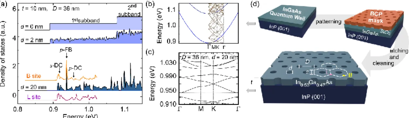
Figure 1. Band structure engineering upon the periodic nanoperforation of a quantum well. (a) Variation of the conduction-band density of states of an In0.53Ga0.47As quantum well grown on a
InP (001) substrate, which is nanoperforated with increasing pore sizes. The thickness t of the quantum well, the periodicity D of the lattice and the diameter d of the pores are indicated. The local density of states at the lattice (L) and bridge (B) sites are superimposed to the (total) density of states for a pore diameter of 20 nm. Vertical arrows point to key features of the density of states, such as Dirac cones (DC) and a flat band (FB). The energy reference is the top of the bulk valence band. (b) Band structure of the quantum well in the first Brillouin zone and in the reduced zone scheme obtained for a periodicity of 36 nm in the real space. (c) Band structure of the nanoperforated quantum well. (d) Illustration of the fabrication process using a self-assembled block copolymer (BCP) thin film as a mask to obtain a honeycomb lattice with a lattice constant a = D/3.
As a model III-V semiconductor heterostructure, we consider here a 10 nm-thick In0.53Ga0.47As QW grown by molecular beam epitxy (MBE) on an InP (001) substrate. As shown
in Figure 1, band theory predicts that the step-like 2D density of states (DOS) of the QW in the conduction band gets featured upon its perforation with tiny pores arranged in a triangular lattice with a periodicity D of 36 nm. This arises from the interplay between band folding in the Brillouin zone of the superlattice and the gap opening at the edges or at the centre of the Brillouin zone due to scattering of the electronic waves by the periodic potential of the pores (Figure 1(b)). As the pore size increases, these features get more pronounced and separate in energy due to a stronger lateral confinement (Figure S3). At a pore diameter d of 20 nm, the DOS consists of well separated mini-bands (Figure 1(c)). This triangular lattice of pores is equivalent to a honeycomb lattice with
a lattice constant a=D/3 ~ 21 nm. In this honeycomb lattice, we can conceptually define lattice sites at the barycenter of three adjacent pores. Each such lattice site can be considered as a quantum dot, characterized by s and px,y-orbitals in the lowest part of the spectrum, the pz orbitals being
only involved in the high-energy states coming from the second subband of the QW. If s-p hybridization can be avoided, the electronic coupling between the lattice sites leads to two dispersive s-bands forming a Dirac cone, and a set of four px,y-orbital bands. Among the latter
bands, the two dispersive px,y-bands form Dirac cones (DC) at the K points, with a flat-band
beneath the DC, and one above. The hexagonal symmetry is not compatible with the orthogonal in-plane px,y-orbitals, resulting in destructive interferences and the creation of FBs.15 Due to the
p-orbital character, the FBs should give rise to a strong peak in the local density of states (LDOS) at positions between the lattice sites (which we will call bridge sites) and zero-density of states on the lattice sites themselves (Figure 1(a) and Figure S5). Crucial to the existence of the lower p-orbital FB is the energy separation with the s-band, which takes place for ratios d/D higher than 0.5 (Figures S4 and S6). At this stage, a major question is to what extent the disorder in the lattice will cloud the existence of such a FB. Despite numerous theoretical predictions of the influence of disorder on specific energy-momentum dispersions obtained with translationally invariant Hamiltonians,16,17,18 the actual fate of the FB is still unknown, as a gradual increase of disorder can
lead first to the destruction of specific momentum-dispersions and then to their reappearance.19
Aiming at engineering well-separated mini-bands with pure orbital character and band gaps larger than the thermal fluctuations at room temperature (25 meV), our approach takes advantage of the wafer-scale and low-cost self-assembled block copolymer (BCP) lithography.20 This
technique enables the creation of a honeycomb lattice in an In0.53Ga0.47As/InP heterostructure QW
with a lattice constant of 21 nm. Moreover, the selective removal of the (poly)methylmethacrylate (PMMA) domains in the BCP leads to a poly(styrene) (PS) honeycomb mask with an intended mean pore size of 20 nm, yielding a ratio d/D of 0.56 for a periodicity of 36 nm. While such a ratio is suitable for the creation of a FB, it also renders the s-DC bandwidth to 7 meV at the M points of the Brillouin zone (Figure S4). Direct access to the local density of states (LDOS) in the lattice is obtained with scanning tunnelling spectroscopy (STS), which has beautifully revealed the existence of FBs in 2D atomic crystals21,22,23 or atomic and molecular lattices on metal surfaces7,8,9.
The STS results that we present on the In0.53Ga0.47As honeycomb lattice show not only the
Comparison with tight binding calculations, which are particularly suitable to take into account the effect of a random disorder on the lattice sites, reveals that the lattice imperfections perturb the bands, but does not erase them. Especially, the flat band is omnipresent on all bridge sites of the honeycomb lattice, even for imperfections producing local potential fluctuations of ± 5 meV, an energy perturbation comparable to the designed width of the dispersive bands and gaps.
The top-down patterning methodology to produce the honeycomb lattice is illustrated in Figure 1(d) and, with more details, in Figure S10. The plasma-enhanced chemical vapour deposition of a 16 nm-thick SiO2 layer on the QW, prior to the spin coating of the BCP thin film,
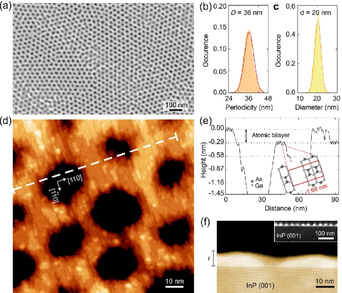
warrants a successful pattern transfer to the In0.53Ga0.47As QW. As seen in Figure 2(a), after the
removal of this protective layer, the QW shows periodic pores, arranged into the micro-domain structure of the BCP mask (Figure S11). The generated antidot lattice has a periodicity of D = 36.0 ± 2.8 nm and a pore size of d = 20.0 ± 1.4 nm (Figure 2(b, c)). As the deposition of the SiO2 layer
leads to the oxidation of the QW surface, which is further altered by the etching of the SiO2 mask
at the end of the whole workflow, a cleaning of the surface with atomic hydrogen and As4 flux
was performed in the MBE chamber.24 It was followed by a thin amorphous As capping,25 which
is essential to recover a clean and well-ordered In0.53Ga0.47As (001) surface,26 as demonstrated in
the STM image of Figure 2d. The surface structure is similar to the one observed on the surface of the pristine QW (Figure S12), consistent with an As-rich (2x4) surface. Although the STM tip is not sharp enough to reach the bottom of the pore, cross-sectional scanning transmission electron microscopy (STEM) of the heterostructure indicates the full perforation of the QW (Figure 2(f)).
Figure 2. Structural properties of the nanoperforated In0.53Ga0.47As quantum well. (a) SEM image
showing the successful pattern transfer. (b) and (c), Distributions of the pore periodicity and pore diameter measured from SEM images. (d) Atomically-resolved STM image of the nanoperforated In0.53Ga0.47As (001) surface, showing variability in the pore size and height of the lattice sites. (e)
Height profile measured along the dash segment of the STM image. The corrugation seen on the atomic terraces arises from the As-rich (2x4) reconstruction, which is highlighted in the graph. (f) High resolution cross-sectional high angle annular dark field STEM image of the nanoperforated heterostucture. Inset: Larger cross-sectional view.
Figure 3. Spatially-resolved scanning tunnelling spectroscopy of the honeycomb lattice. (a) topographic and (b) spectroscopic measurements at varying positions across two adjacent lattices via a bridge site, labelled L1, L2 and B respectively. The vertical segment indicates the position of
the p-orbital flat band, whereas the arrows point to spectral features of the s and p-dispersive bands. The dotted line spectrum was measured on the pristine QW for comparison. Inset: Magnified view on the spectral region showing the s and p-flat bands at the bridge site. (c) Contour followed by the STM tip scanning at constant height between the acquisition of the spectra. The electronic coupling of the tip states with the wave function Ψs of the antidot lattice depends on the thickness of the lattice sites L1 or L2. (d) Check of the occurrence of the p-orbital FB peak on the bridge site
concomitant with its absence on the adjacent lattice site in four regions of the sample. Insets: STM images of the corresponding regions, which show various degrees of patterning disorder.
In order to resolve the DOS in the conduction band, the QW was doped with Be at a concentration higher than 1019 cm-3. The large hole density in the QW ensures the fast
recombination of the tunnelling electrons, avoiding in this way any charging of the QW. Above all, the dense hole gas minimizes the potential fluctuations caused by the random distribution of charged impurities and defects.26 Efficient screening is preserved, even after nanoperforation of
band with deviations smaller than 85 meV for remote regions of the sample (Figure S12). A mean position of the Fermi level of 160 ± 11 meV above the valence band edge indicates a low density of defects, which is remarkable in view of the technological processes in the nanopatterning. Spatially-resolved tunnelling spectra were first acquired on positions between two lattice sites (Figure 3(a)). Right at the bridge site (B), the differential conductance spectrum reveals a strong peak centred at 788 ± 3 meV, with two tiny shoulders pointed by arrows at smaller bias (770 meV and 754 meV) and another one at higher bias (798 meV) (Figure 3(b)). The peak gradually vanishes away from the bridge site, and is absent at the lattice sites L1, L2. On the honeycomb lattice site L2,
a doublet appears at lower energy, and this is also the case for the position next to the lattice sites
L2 and L1. At position L1 and further away from L1, we do not detect any signal below 800 meV.
As shown in Figure 3(c), we observe a height difference of two bilayers between lattice sites L1
and L2, very probably the reason that the peak doublet cannot be observed at position L1 and away
from L1 with the chosen STS feedback parameters (Figure S13).
A careful analysis of the surface corrugation (Figures 2(a), 3(a) and Figure S14) reveals that the etching of the QW is usually more pronounced at the bridge sites, making the centre of mass of the square wave function of the confined states closer to the surface and allowing a stronger coupling of these states with the tip states. Focussing the STS measurements in the vicinity of bridge sites for many other regions of the sample, some of them being separated by hundreds of micrometers from each other, we consistently measured a strong peak at the bridge sites gradually vanishing and disappearing 2-3 nm away from the bridge site (Figure 3(d) and Figure S13). In line with the theoretical predictions of Figure 1(a) and Figure S5, we assign this peak to the lowest p-orbital FB (notice the energy shift as the experimental reference is given by the position of the Fermi level). Then, the lower-energy peak doublet at (and close to) the lattice sites should correspond to the s-orbital Dirac cone; the peak maxima reflecting the maximum LDOS at the M points. We observe a strong variation in the shape and peak separation of this doublet. For instance, the energy difference between the two maxima is often substantially larger than the 7 meV expected for an ideal honeycomb lattice.
The structural analysis of the nanoperforated QW reveals obvious variation in the pore geometry and in the thickness t of individual lattice sites. The conical shape of the pores does not significantly affect the band structure.14 But variation in the thickness and deviations from the ideal
impact on the s and p-orbital on-site energies and the coupling between two adjacent sites. Calculation of the increase of confinement due to a bilayer reduction, as observed in Figure 2(e), yields an energy of 5.6 meV for the s-state. Similarly, calculations of the s on-site energies and of the hopping integral between the s and p orbitals show an increase of the on-site energy by 3.4 meV and a reduction of the hopping integral by 1.2 meV as the ratio d/D increases from 0.55 to 0.60 (Figure S7). These energy variations have a magnitude in the same order as the separation between the s-orbital doublet and the FB peak, and the peak separations observed in the s-orbital doublet. We are hence in a situation in which disorder affects the energetics but does not cloud the intrinsic band features of the lattice.
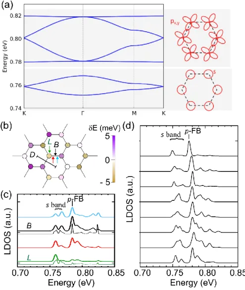
lattice, with a periodicity D, comprising 477 sites, that is used to determine the influence of disorder. On each site (L), a random potential perturbation δE is applied to the on-site energies ES and EP. (c) Local density of states calculated along the connection bridging two lattice sites at the positions marked with arrows in (b). The black and green thin curves, calculated at the bridge (B) and lattice (L) sites in the absence of disorder, are used as references. (d) Representative LDOS calculated for eight different bridge sites, which show the robustness of the p-FB peak and the variability of the dispersive s bands. The reference in energy has been aligned with respect to the experimental Fermi level pinning, 160 meV above the top of the valence band. All the curves, except the reference ones in (c), were convoluted with a Gaussian function to account for the bias modulation of 3 meV.
Gaining a more accurate understanding of the influence of disorder was achieved by considering a simple (effective) tight-binding Hamiltonian, where each site of the honeycomb lattice is described by one s and two in-plane px,y-orbitals (see Methods in the Supporting
Information). For that purpose, the electronic structure of the ideal honeycomb lattice was first calculated with an effective mass approximation (EMA) and compared with a fully atomistic tight-binding calculation. Good agreement between both calculations was obtained when non-parabolic corrections were included in EMA. The parameters of the simple tight-binding Hamiltonian, defined by two on-site energies ES and EP and four nearest-neighbour hopping parameters were
then derived from the fit of the band structure calculated with the EMA model (Figure 4(a)). As the on-site energies are more affected by the structural disorder than the hopping terms (Figure S7), a random energy perturbation was applied on ES and EP of each site to explicitly inform on
the effect of disorder (Figure 4(b)). The amplitude of the on-site energy variation was raised by steps of 1 meV. For an amplitude of ± 5 meV, which is in line with the observed structural disorder, the LDOS calculated between two particular lattice sites shows that the disorder has only minute effects on the p-orbital FB (Figure 4(c)). The simulated disorder has more effect on the peak doublet of the s-orbital Dirac cone. It pulls the peaks in the first doublet (M points of the s band) further apart, adding 4 meV to their natural separation. Calculations for tens of different sites (Figure 4(d) and Figure S8) shows a substantial variation in the doublet peak shapes and peak separation for the dispersive bands, whereas the p-FB is preserved. Moreover, the simulated disorder shifts states of the dispersive p-band towards the p-FB. These effects are in line with the
experimental observations. We simulate a spatial variation in the energy of the p-FB of 8 meV, while the experimental variation is around 19 meV in Figure 3(c). We attribute this difference between simulations and experiment to small variations of the Fermi level pinning. Indeed, a variation in the position of the Fermi level induces a long-range potential shift, which is not included in the calculations. The resilience of the FB peak to disorder is attributed to the combination of several effects detailed in the SI. The main one is that FB states can be described as localized states on hexagonal plaquettes.15 It can be shown that the coupling of these states with
the other states induced by the disorder is weak so that the broadening of the FB peak comes essentially from the average disorder potential in these states which, given the large number of states available in this band, results in a LDOS peak that remains very strongly marked.
To conclude, using the honeycomb lattice as a prominent example, we presented the basis of a future technological platform for III-V semiconductor heterostructures in which the band structure can be engineered by nanoperforation with lattice constants ~ 20 nm. The intrinsic honeycomb resonances are perturbed by nanoscale disorder, but still remain visible over the entire honeycomb structure. In contrast to the s-orbital Dirac cone, which was not unambiguously resolved in the tunnelling spectra, the p-orbital flat band, arising from the interference of in-plane
p-orbitals, is an intrinsic lattice resonance that is strongly resilient against the disorder induced by
imperfect nanoperforation. Combining well-known semiconductor heterostructures that allow for electronic gating with band-engineering by nanopatterning is one of the most rational paths toward exotic states and topological protection.
ASSOCIATED CONTENT
Supporting Information. The Supporting Information are available free of charge.
Whole electronic structure calculations; details of the sample fabrication; additional scanning tunneling spectroscopic measurements.
AUTHOR INFORMATION Corresponding Author
*[email protected]; [email protected]; [email protected]; [email protected].
Author Contributions
C.D., B.G., D.V., X.W., T.X. conceived and instructed the research; N.F with the assistance of C.C., L.D. C.P., F.V., X.W., D.Y. fabricated the samples; G.F. performed BCP lithography; Y.L., C.P., G.P., D.T., T.X. analysed the samples with electron microscopies; N.F., B.G., C.P., D.S. performed the STM experiments and processed the data; C.D. and C.P. gave the theoretical analysis; C.D., B.G., D.V. wrote the manuscript, with input from all authors.
⊥These authors contributed equally.
ACKNOWLEDGMENT
We thank D. Stiévenard for fruitful discussions. We gratefully acknowledge Arkema and Digital Surf for providing the materials to prepare the block copolymer mask and routines to process the STS data. Funding: This work was supported by the French National Research Agency (Dirac III-V project ANR-16-CE24-0007-01, Germanene project ANR-17-CE09-0021-03), the EQUIPEX program Excelsior (Grant No. ANR-11-EQPX-0015), the RENATECH network, the H2020 program (ERC Advanced Grant 692691-“FIRST STEP”), the Dutch Research Council (NWO Chemistry - Toppunt “Superficial superstructures”) and the Natural Science Foundation of Shanghai (19ZR1419500).
REFERENCES
(1) Leykam, D.; Andreanov, A.; Flach, S. Artificial flat band systems: from lattice models to experiments. Advances in Physics: X 2018, 3, 1473052.
(2) Bistritzer, R.; MacDonald, A. H. Moiré bands in twisted double-layer graphene. PNAS 2011, 108, 12233-12237.
(3) Wu, C.; Bergman, D.; Balents, L.; Sarma, S. D. Flat bands and Wigner crystallization in the honeycomb optical lattice. Phys. Rev. Lett. 2007, 99, 070401.
(4) Jacqmin, T.; Carusotto, I.; Sagnes, I.; Abbarchi, M.; Solnyshkov, D. D.; Malpuech, G.;
Galopin, E.; Lemaître, A. ; Bloch, J. ; Amo, A.Direct observation of Dirac cones and a flatband
in a honeycomb lattice for polaritons. Phys. Rev. Lett. 2014, 112, 116402.
(5) Mukherjee, S.; Spracklen, A.; Choudhury, D.; Goldman, N.; Öhberg, P.; Andersson, E.; Thomson, R. R. Observation of a localized flat-band state in a photonic Lieb lattice. Phys. Rev. Lett. 2015, 114, 245504.
(6) Taie, S.; Ozawa, H.; Ichinose, T.; Nishio, T.; Nakajima, S.; Takahashi, Y. Coherent driving and freezing of bosonic matter wave in an optical Lieb lattice. Science Adv. 2015, 1, e1500854.
(7) Drost, R.; Ojanen, T.; Harju, A.; Liljeroth, P. Topological states in engineered atomic lattices. Nat. Physics 2017, 13, 668-671.
(8) Slot, M. R.; Gardenier, T. S.; Jacobse, P. H.; van Miert, G. C.; Kempkes, S. N.;
Zevenhuizen, S. J. M.;Morais Smith, C.; Vanmaekelbergh, D.; Swart, I. Experimental realization
and characterization of an electronic Lieb lattice. Nat. Physics 2017, 13, 672-676.
(9) Gardenier, T.; van den Broeke, J.; Moes, J.; Swart, I.; Delerue, C.; Slot, M.; Morais Smith, C.; Vanmaekelbergh, D. p Orbital Flat Band and Dirac Cone in the Electronic Honeycomb Lattice
Article. ACS Nano 2020, 5.
(10) Cao, Y.; Fatemi, V.; Demir, A.; Fang, S.; Tomarken, S. L.; Luo, J. Y.; Sanchez-Yamagishi, J.D.; Watanabe, K.; Taniguchi, T.; Kaxiras, E.; Ashoori, R. C.; Jarillo-Herrero, P. Correlated insulator behaviour at half-filling in magic-angle graphene superlattices. Nature 2018, 556, 80-84.
(11) Gibertini, M.; Singha, A.; Pellegrini, V.; Polini, M.; Vignale, G.; Pinczuk, A.; Pfeiffer, L. N.; West, K. W. Engineering artificial graphene in a two-dimensional electron gas. Phys. Rev. B 2009, 79, 241406.
(12) Wang, S.;Scarabelli, D.; Du, L., Kuznetsova, Y. Y.; Pfeiffer, L. N.; West, K. W.; Gardner, G. C.; Manfra, M. J. ; Pellegrini, V.; Wind, S. J.; Pinczuk, A. et al., Observation of Dirac bands in artificial graphene in small-period nanopatterned GaAs quantum wells. Nat. Nanotechnology 2018, 13, 29-33.
(13) Tadjine, A.; Allan, G.; Delerue, C. From lattice Hamiltonians to tunable band structures by lithographic design. Phys. Rev. B 2016, 94, 075441.
(14) Post, L. C.; Xu, T.; Vergel, N. F.; Tadjine, A.; Lambert, Y.; Vaurette, F.; Yarekha, D.; Desplanque, L.; Stiévenard, D.; Wallart, X.; Grandidier, B. Delerue, C.; Vanmaekelbergh, D.
Triangular nanoperforation and band engineering of InGaAs quantum wells: a lithographic route
toward Dirac cones in III–V semiconductors. Nanotechnology 2019, 30, 155301.
(15) Wu, C.; Sarma, S. D. px,y-orbital counterpart of graphene: Cold atoms in the honeycomb optical lattice. Phys. Rev. B 2008, 77, 235107.
(16) Bodyfelt, J. D., Leykam, D., Danieli, C., Yu, X.; Flach, S. Flatbands under correlated
perturbations. Phys. Rev. Lett. 2014, 113, 236403.
(17) Soriano, D.; Ortmann, F.; Roche, S. Three-dimensional models of topological insulators: Engineering of dirac cones and robustness of the spin texture. Phys. Rev. Lett. 2012, 109, 266805.
(18) Bilitewski, T.; Moessner, R. Disordered flat bands on the kagome lattice. Phys. Rev. B
2018, 98, 235109.
(19) Schubert, G.; Fehske, H.; Fritz, L.; Vojta, M. Fate of topological-insulator surface states under strong disorder. Phys. Rev. B 2012, 85, 201105.
(20) Suh, H. S.; Moni, P.; Xiong, S.; Ocola; L. E.; Zaluzec, N. J.; Gleason, K. K.; Nealey, P. F. Sub-10-nm patterning via directed self-assembly of block copolymer films with a vapour-phase deposited topcoat. Nat. Nanotechnology 2017, 12, 575-581.
(21) Xie, Y.; Lian, B., Jäck, B., Liu, X., Chiu, C. L., Watanabe, K.;Taniguchi, T.; Bernevig, B. A.; Yazdani, A. et al., A. Spectroscopic signatures of many-body correlations in magic-angle twisted bilayer graphene. Nature 2019, 572, 101-105.
(22) Zhang, Z.; Wang, Y.; Watanabe, K.; Taniguchi, T.; Ueno, K.; Tutuc, E.; LeRoy, B. J. Flat bands in twisted bilayer transition metal dichalcogenides. Nat. Physics, 2020.
(23) Mao, J.;Milovanović, S. P.; Anđelković, M.; Lai, X.; Cao, Y.; Watanabe, K.;Taniguchi, T.; Covaci, L.; Peeters, F. M.; Geim, A. K.; Andrei E. Y. Evidence of Flat Bands and Correlated
(24) Fahed, M.; Desplanque, L.; Troadec, D.; Patriarche, G.; Wallart, X. Selective area
heteroepitaxy of GaSb on GaAs (001) for in-plane InAs nanowire
achievement. Nanotechnology 2016, 27, 505301.
(25) Xu, T.; Dick, K. A.; Plissard, S.; Nguyen, T. H.; Makoudi, Y.; Berthe, M.; Nys, J.P.;
Wallart, X.; Grandidier, B.; Caroff, P.Faceting, composition and crystal phase evolution in III–V
antimonide nanowire heterostructures revealed by combining microscopy
techniques. Nanotechnology 2012, 23, 095702.
(26) N. A. Franchina Vergel, Tadjine, A.; Notot, V.; Mohr, M.; N’Guissan, A.K.; Coinon, C.; Berthe, M.; Biadala, L.; Sossoe, K. K.; Dzagli, M. M.; Girard, J.-C.; Rodary, G.; Desplanque, L.; Berndt, R.; Stiévenard, D.; Wallart, X.; Delerue, C.; B. Grandidier, Influence of doping level and surface states in tunneling spectroscopy of an In0.53Ga0.47As quantum well grown on p-type doped