HAL Id: hal-02352233
https://hal.univ-lorraine.fr/hal-02352233
Submitted on 6 Nov 2019
HAL is a multi-disciplinary open access
archive for the deposit and dissemination of
sci-entific research documents, whether they are
pub-lished or not. The documents may come from
teaching and research institutions in France or
abroad, or from public or private research centers.
L’archive ouverte pluridisciplinaire HAL, est
destinée au dépôt et à la diffusion de documents
scientifiques de niveau recherche, publiés ou non,
émanant des établissements d’enseignement et de
recherche français ou étrangers, des laboratoires
publics ou privés.
Synthesis of CdO nanostructures by nano-second pulsed
discharges in liquid nitrogen
M Trad, A. Nomine, J. Ghanbaja, C. Noël, M. Tabbal, T. Belmonte
To cite this version:
M Trad, A. Nomine, J. Ghanbaja, C. Noël, M. Tabbal, et al.. Synthesis of CdO nanostructures by
nano-second pulsed discharges in liquid nitrogen. 24th International Symposium on Plasma Chemistry
(ISPC 24), Jun 2019, Naples, Italy. �hal-02352233�
Synthesis of CdO nanostructures
by nano-second pulsed discharges in liquid nitrogen
M. Trad1, A. Nomine1, J. Ghanbaja1, C. Noel1, M. Tabbal2, T. Belmonte11Université de Lorraine, Institut Jean Lamour, UMR7198 CNRS, Nancy, France 2Department of Physics, American University of Beirut, Riad El Solh 1107 2020, Beirut, Lebanon
Abstract: In this work, we report on the synthesis of Cd nanostructures by nano-second
pulsed electrical discharges generated between two pure cadmium electrodes in liquid nitrogen. These nanostructures are oxidized in air after evaporation of the cryogenic liquid, leading to CdO. An investigation of the effect of discharge voltage on the synthesis process was conducted. Transmission Electron Microscopy analyses show that, contrary to other metallic nanoparticles synthesized by the same process, CdO nanoparticles self-assemble to give hollow micrometric cubes that transform into bunches of nanowires when the applied voltage increases. Time-resolved optical emission spectroscopy performed on the discharge during synthesis shows the presence of ionic and neutral Cd species in the discharges. A growth mechanism of Cd objects along the electric field lines in the discharge is proposed.
Keywords: cadmium, discharges in liquid, nanoparticles, nanowires
1.Introduction
Research on plasma discharges generated in liquids have experienced a renewed interest in the last decade owing to the potential applications such discharges can have in a wide variety of rapidly evolving technological fields such as water treatment, sterilization, materials processing and nanoparticles synthesis [1, 2]. In the latter, plasma discharges are particularly attractive because they allow the synthesis of nanoparticles with typical diameter of the order of 20 nm and lower, at significantly high yield rates reaching several hundred grams per hour [3]. A variety of carbonaceous and non-carbonaceous nanoparticles have thus been obtained, in polar and non-polar liquids under different electrical conditions and geometries, but a major challenge is the control of the size and shape of the nanoparticles and their stoichiometry in the case of compound materials such as alloys bimetals and semiconductor oxides. One such semiconductor oxide that has recently attracted much interest lately is cadmium oxide (CdO). It is an n-type semiconductor with a face-centered-cubic (fcc) crystal structure and a direct band gap of 2.2 to 2.5 eV. CdO, under nanostructured form, whether as nanoparticles or as hollow nanoshapes exhibit low density, high surface area, and distinct optical property making it a promising candidate for applications in catalysts, sensors, nonlinear materials, solar cells, and other optoelectronic devices. Several authors have indeed recently reported on the synthesis of cadmium oxide nanoparticles by laser ablation in a liquid environment [4], microwave irradiation [5], microwave assisted techniques [5, 6] as well as a variety of solvent based techniques [7-9].
In this work, we report on the synthesis of cadmium oxide nanostructures synthesized by electrical discharges generated between two cadmium electrodes immersed in
liquid nitrogen. The obtained nanoparticles were investigated by High-Resolution Transmission Electron Microscopy (HR-TEM), micro-Energy Dispersive X-ray (EDX) analyses whereas the process was characterized by current voltage measurements on the discharge and time-resolved optical emission spectroscopy. The structural properties of the nanoparticles and the discharge diagnostics were correlated in order to better understand the formation of the CdO nanostructures.
2.Experimental
The experimental set-up used in this work is a pin-to-pin electrode configuration that is described in details elsewhere [10]. Briefly, a high DC voltage power supply (Technix SR15-R-1200—15 kV— 80 mA) feeds a high voltage solid-state switch (HTS-301-03- GSM), that is in turn connected to one of the pin-electrodes while the other is grounded. The two electrodes are identical, made of cadmium (cut from pure Cd wires) with a diameter of 1 mm. The polished and sharpened tips of the electrodes are placed facing each other and are dipped in an open Dewar having a volume of about 100 cm3. The Dewar is filled with liquid nitrogen (purity 99.995%, Air Liquide) and the gap between the electrodes is adjustable with a micrometric screw but was fixed at 3 mm in this work. Discharges in the liquid were thus generated by pulsing the DC power supply at a frequency of 10 Hz, for a certain amount of time that can exceed one hour. The nanoparticles that are generated in the process are collected by sedimentation on a carbon TEM grid placed at the bottom of the Dewar underneath the electrodes. At the end of the experiment, the high voltage is switched off and the liquid nitrogen is left to evaporate so that the grid, with the nanoparticles resting on it, can be removed from the Dewar. In this work, several experimental parameters were varied, namely the applied voltage, from 4 to 10 kV,
the discharge pulse width 75 to 2500 ns, and the total processing time from 15 to 60 minutes. A Philips CM200 device and a JEOL ARM 200F Cold FEG device were used for TEM investigation in order to study the crystallinity and the chemical composition of nanoparticles. Optical emission spectroscopy was performed on the discharges with a 550 mm focal length monochromator (Jobin-Yvon TRIAX 550) equipped with a 100 gr.mm−1 grating for overall spectra in the 250–900 nm. It was coupled with a HORIBA Jobin-Yvon i- Spectrum Two ICCD detector. Each measurement is averaged over 50 spectra recorded with an exposure time of 50 ns. Electrical data from the discharge were acquired with two voltage probes. The first probe is set after the ballast resistor, and it is used to determine the voltage applied to the discharge. The second probe is set after the discharge. As a voltage is measured, another resistor is used to calculate the current.
3.Results and discussion
Fig. 1 shows representatives TEM images of nanostructures synthesized for a pulse duration of 100 ns at three different voltages 4, 7 and 10 kV, for a total synthesis time of one hour. At 4 kV (Fig. 1 (a)), well-faceted crystallites are obtained in agreement with reports of similar shapes of high quality cadmium oxide with flat surfaces and sharp edges obtained by thermal decomposition of cadmium carbonate. Typical sizes of these particles are a few hundred microns, and many of them appear cube-shaped as seen in the inset of Fig. 1 (a). Increasing the discharge voltage to 7 kV produces significantly different shapes, as shown in Fig. 1 (b), where the formation of bowtie-like nanoparticles is detected. The inset of Fig. 1 (b) shows a zoomed image of a particle where clearly directional nanowire growth has taken place emanating from the core of the particle, thus leading to the bowtie-like shape. Directional growth of nanowires is further evidenced in Fig. 1 (c) where it is seen that the synthesis product consists essentially of nanowires and remains of particles from which nanowires originate.
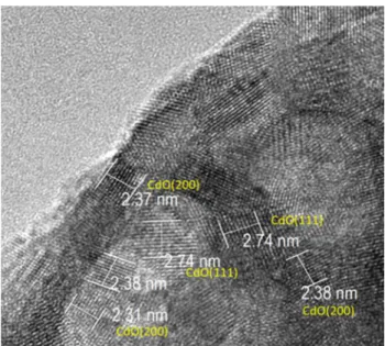
High resolution TEM analyses were performed on cubes grown at 4 kV (Fig. 1a). It was found that cubes are made of stacked up nanoparticles. Indeed, in the example given in Fig. 2 where an isolated cube is depicted, the structure appears porous in close-up images of the edge of the nanocube. Nanocrystalline domains, whose sizes range between 2.3 and 2.7 nm are marked in the figure. These randomly oriented nanocrystalline domains were identified through unreported electron diffraction patterns that confirm the presence of CdO (111) (200) and (220) planes. Micro-EDX measurements on these cubes show that their stoichiometry is Cd 55 at.% O 45 at.%, within an accuracy of ±5%, thus confirming that these are impurity-free CdO nanoparticles. It is noteworthy to recall that the starting electrodes in the process are made of pure Cd, and therefore the presence of oxygen in the
nanoparticles could only be attributed to an oxidation of the metal after liquid nitrogen is fully evaporated at the end of the experiments. The porous nature of the synthesized particles, as observed by TEM imaging, shown above would play a significant role in ensuring a nearly complete oxidation of the Cd structure, as deduced from EDX measurements while a crystalline structure is still maintained.
CdO nano-objects look visibly "stretched" when the applied voltage increases. This means that their initial cubic shape – we checked that these objects were 3D and not 2D– evolves towards the shape of an elongated object with cube corners getting filamentary, as visible in Fig. 1 (c).
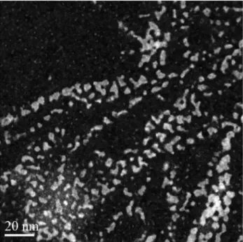
On the other hand, STEM high-angle annular dark-field (HAADF) images of wires (Fig. 3) show that wires are assembly of particles with sizes close to 3-4 nm. Unreported high-resolution TEM analyses show that these nanoparticles have cubic shapes.
Fig. 1. Nanostructures synthesized for a pulse duration of 100 ns at three different voltages a) 4, b) 7 and c) 10 kV,
for a total synthesis time of one hour.
Fig. 2. High resolution TEM image of one edge of the nanocube depicted in Fig. 1.
Fig. 3. STEM HAADF image of a bunch of CdO wires as those in Fig 1.
We thus confirm that both kinds of structures are obtained by assembly of the same kind of elementary nanocubes, assembly whose anisotropy is enhanced by the intensity of the applied electric field.
Further insight on the growth of the nanoparticles and nanowires in our process were deduced from time resolved optical emission spectroscopy. In Fig. 4, we show spectra from the discharge operated at 4, 7 and 10 kV and the corresponding identification of line transitions (see Table 1 for a list). First, it is important to notice that emission lines are strongly broadened, shifted and sometimes distorted (their shape becomes asymmetric) especially at the beginning of the discharge because of the important contribution of the Stark effect, which is due to the high electron density in the discharge (typically around 1016 cm−3) [10]. The presence of both the Cd I and Cd II systems is easy to admit.
For the 4 kV spectrum, the emission is somewhat weak and can be solely attributed to Cd neutral atomic lines. Expectedly, emission becomes stronger at higher voltages but more importantly, lines that correspond to emission from Cd+ ions are identified. In addition, no emission from nitrogen lines are detected at any of three discharge voltages used, as reported in other work involving discharges in liquid nitrogen [11].
From the inspection of TEM analyses and OES measurements, we observe that the detection of Cd+ ions in the discharges generated at 7 and 10 kV seems to be correlated with the formation of nanowires, (see Figures 1 (b) and 1 (c)). Such a correlation could provide an explanation for the formation of nanowires, resulting from the presence of ions that might play a role in a mechanism of anisotropic growth along the electric field lines. This aspect is further discussed below.
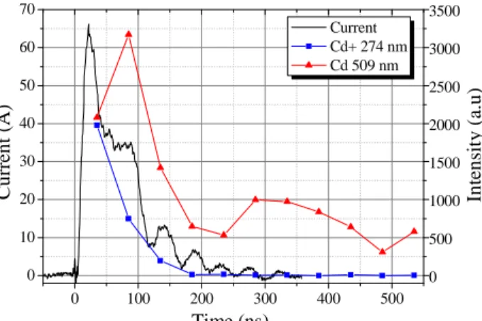
Time-resolved optical emission spectra were recorded with an integration time of 50 ns for pulse widths equal to 100 ns. Discharges were ignited between two electrodes of cadmium for an applied voltage of +10 kV. Thus, in Fig. 5, the time evolution of two selected neutral and ionic lines shows that the former lasts during the temporal afterglow of the discharge whereas the latter stops almost at the end of the discharge.
Table 1: Identified transitions corresponding to emission lines depicted in Fig. 2.
Transition Wavelength (nm) Upper level Lower level Cd II 274.85 6s 2S1/2 5p 2P°3/2 Cd I 346.62 (346.76) 5s5d 3D J=2 5s5p 3P° J=1 Cd I 361.05 (361.28) 5s5d 3D J=3 5s5p 3P° J=2 Cd II 441.56 5s2 2D5/2 5p 2P°3/2 Cd I 467.81 5s6s 3S J=1 5s5p 3P° J=0 Cd I 479.99 5s6s 3S J=1 5s5p 3P° J=1 Cd I 508.58 5s6s 3S J=1 5s5p 3P° J=2 Cd II 533.75 4f 2F°5/2 5d 2D3/2 Cd II 537.81(538.19) 4f 2F°7/2 5d 2D5/2 Cd I 643.84 5s5d 1D J=2 5s5p 1P°
Fig. 4. Optical Emission spectra obtained from the discharge at three different voltages, namely 4, 7 and 10
kV. Emission lines from Cd neutral atoms and Cd+ ions are identified. 300 400 500 600 700 800 2.0x10⁴ 4.0x10⁴ 6.0x10⁴ 8.0x10⁴ 1.0x10⁵ 1.2x10⁵ Cd Cd Cd Cd+ In te n si ty ( a. u .) Wavelength (nm) 4 kV 7 kV 10 kV Cd+ Cd+
Fig. 5. Time resolved optical emission spectroscopy for a 100 ns discharge operated at 10 kV and (b) evolution of the Cd+ (274 nm) and the Cd (509 nm) lines as a function of time. The time evolution of the current in the discharge
is also shown.
We observed from unreported results, that increasing the discharge time from 100 ns to 2500 ns at a given voltage does not change significantly the shape of objects but their density. Elementary nanocubes do not stay within the high-density plasma region but likely move outward driven by the pressure gradient, closer to the discharge-liquid boundary, i.e. in the spatial afterglow. They get assembled there, where the electric field lines corresponding to a given intensity are all the more repelled outside as the applied electric field increases. The size of the high-density plasma region is likely dependent on the applied voltage, the higher the intensity, the larger the discharge radius. Thus, we may expect a slight increase in the size of elementary nanocubes at high fields, which seems to be the case.
Consequently, the progressive change of the shape of the cubes into elongated structures is attributed to the role of the electric field on elementary nanocubes mainly grown from the vapour emitted during the melting of the electrode.
In Fig. 5, we notice that the burst of neutral Cd species occurs slightly before 100 ns. This is coherent with former calculations [10] where we showed that the area of the electrode struck by the discharge reaches 1000 K typically after about 200 ns, the melting point of Cd being close to 594 K.
To sum up, a schematic of the growth mechanism of Cd wires is proposed in Fig. 6.
Fig. 6. Proposed growth mechanism of Cd wires.
4.Acknowledgments
This work benefited from the support of the project CEENEMA ANR-15-CE05-0005-01 of the French National Research Agency (ANR). MT would like to thank the French Embassy in Beirut for a SAFAR fellowship.
5.References
[1] P. Bruggeman, C. Leys, Journal of Physics D: Applied Physics, 42, 053001 (2009).
[2] W. G. Graham, K. R. Stalder, Journal of Physics D: Applied Physics, 44, 174037 (2011).
[3] T. Belmonte, A. Hamdan, F. Kosior, C. Noël, G. Henrion, Journal of Physics D: Applied Physics, 47, 224016 (2014).
[4] A. M. Mostafa, S. A. Yousef, W. H. Eisa, M. A. Ewaida, E. A. Al-Ashkar, Optik-International Journal for Light and Electron Optics, 144, 679 (2017).
[5] D. S. Raj, R. Jayaprakash, T. Prakash, G. Neri, T. Krishnakumar, Applied Surface Science, 266, 268 (2013).
[6] N. C. S. Selvam, R. T. Kumar, K. Yogeenth, L. J. Kennedy, G. Sekaran, J. J. Vijaya, Powder technology, 211, 250 (2011).
[7] L. Beigi, V. Saheb, Nano-Structures & Nano-Objects,
9, 13 (2017).
[8] H. Yu, D. Wang, M. Y. Han, Journal of the American Chemical Society, 129, 2333 (2007).
[9] P. S. Kumar, M. Selvakumar, S. G. Babu, S. Karuthapandian, S. Chattopadhyay, Materials Letters, 151, 45 (2015).
[10] A. Hamdan, F. Kosior, C. Noël, G. Henrion, J.-N. Audinot, T. Belmonte, Journal of Applied Physics,
113, 213303 (2013).
[11] H. Kabbara, J. Ghanbaja, C. Noël, T. Belmonte, Materials Chemistry and Physics, 207, 350 (2018). [12] T. Belmonte, C. Noël, T. Gries, J. Martin, G.
Henrion Plasma Sources Science and Technology,
24, 064003 (2015). 0 100 200 300 400 500 0 10 20 30 40 50 60 70 Current Cd+ 274 nm Cd 509 nm Time (ns) C u rr en t (A ) 0 500 1000 1500 2000 2500 3000 3500 I n te n si ty ( a. u )