HAL Id: hal-03002949
https://hal.archives-ouvertes.fr/hal-03002949
Submitted on 13 Nov 2020
HAL is a multi-disciplinary open access
archive for the deposit and dissemination of
sci-entific research documents, whether they are
pub-lished or not. The documents may come from
teaching and research institutions in France or
abroad, or from public or private research centers.
L’archive ouverte pluridisciplinaire HAL, est
destinée au dépôt et à la diffusion de documents
scientifiques de niveau recherche, publiés ou non,
émanant des établissements d’enseignement et de
recherche français ou étrangers, des laboratoires
publics ou privés.
Study on Space Charge Behavior in DC Model Cable
under Thermal Gradient and Polarity Reversal
D Irvandy, H Duong, G. Teyssedre, Laurent Berquez, I Sinisuka, T. Vu
To cite this version:
D Irvandy, H Duong, G. Teyssedre, Laurent Berquez, I Sinisuka, et al.. Study on Space Charge
Be-havior in DC Model Cable under Thermal Gradient and Polarity Reversal. 9th Internat. Symposium
on Electrical Insulating Materials (ISEIM), Waseda University, Tokyo, Japan, 13-17 Sept. 2020, Sep
2020, Tokyo, Japan. pp. 309-312. �hal-03002949�
Study on Space Charge Behavior in DC Model
Cable under Thermal Gradient and Polarity Reversal
D. Irvandy
1*, H.H. Duong
2, G. Teyssedre
2, L. Berquez
2, I. Sinisuka
3, T.T.N. Vu
41 Pt. PLN (Persero), Jakarta, Indonesia 2 Laplace, CNRS and University of Toulouse, France 3 Bandung Institute of Technology, Bandung, Indonesia
4
Electric Power University, Hanoi, Vietnam *E-mail:[email protected]
Abstract – Research on space charge related to HVDC cables is
mostly achieved on small scale samples, being flat specimen or reduced size cables, for questions of cost, easiness and flexibility of tests. Resorting to measurements on model cables, there exist different ways of implementing tests using the pulsed electroacoustic (PEA) method. In this communication we turn back to the different possible arrangements and show that using a dedicated cable loop for applying the voltage pulse can be a suitable way. Some results are shown in presence of a thermal gradient.
Keywords: Space charge, DC, PEA method, polarity reversal, thermal gradient
I. INTRODUCTION
The use of HVDC in electric power transmission systems is becoming increasingly popular because of its advantages compared to HVAC especially for long distance and submarine transmission. Research on HVDC cables especially with regard to insulation is very important because it is related to the reliability and lifetime of the cable itself. Space charge is believed to be the phenomenon responsible for the degradation of insulating material in DC systems.
Most of the studies resorting to research about materials are achieved using small scale samples as working on full size cables is extremely expensive, and does not allow flexibility of the stress to apply on cables. Among samples, flat specimen provided with semiconducting tapes (carbon black doped polymer, semicon) constitutes one way to approach a structure representative of the cable since similar interfaces are reconstituted by co-crosslinking [1]. A second way consists in using cables of reduced size, which brings the cylindrical geometry as well as the possibility to heat the cable through the conductor and form a thermal gradient in the cable, a situation which approaches operating conditions of cables [2]. Therefore, cable samples appear as more realistic samples, even though questions remain: e.g. the amount of crosslinking by-products stored in the cable cannot be fully representative of a thick installation [4].
Model cables used for testing are often either medium voltage (MV) cables, with typically 5-10 mm thick insulation [2] [5], or miniature cables with 1.5 mm insulation thickness [6]. The pulsed electroacoustic –PEA– method is the main method used to probe space charge on cables [6] [7] though Laser-Induced Pressure Pulse [8] or Thermal step method [9] are also used, including on full size cables. Rizzo et al [10] recently reviewed the various principles used to implement the PEA method on cables. They vary according to the degree of intrusively acceptable for cables, and to technical feasibility. In full size cables, the objective will be to minimize the machining achieved on the cable, and an ideal case would be that the full jacket of the cable be maintained.
For small or MV cables, one way to prepare cables consists in removing the semiconducting screen on part of the cable, which can be detrimental to cable withstanding.
In this communication, we discuss different ways of configuring the set-up for measuring space charges in miniature cables having crosslinked Polyethylene (XLPE) as insulation and semicon at both interfaces. We describe an acceptable solution maintaining the integrity of the cable. We illustrate the method by some results obtained under polarity reversal and thermal gradient.
II. EXPERIMENTAL SECTION
A. Cable samples
Samples from model cables, called mini-cables were considered in this research. Mini-cables are special cables that were manufactured for research purposes. With their reduced size, these cables can reduce the cost of production, transportation and testing. They were produced by triple-extrusion (semicon/XLPE/semicon), having a conductor diameter of 1.4 mm, and inner and outer diameter for the insulation of about 1.5 and 3 mm, respectively. With these dimensions, applying 10 kV to the conductor gives geometric electric fields of 10 and 5 kV/mm, respectively at the inner and outer semicon interface.
B. Test configurations
Fig. 1 depicts a very standard way used previously to probe space charges in model cables by PEA [11]. The cable is installed as a loop. A current transformer is used for the purpose of heating the cable through the conductor. In order to apply the voltage pulses while stressing the cable under DC, a decoupling capacitor is necessary. It is realized by removing the semicon on a length of about 5 cm to separate the cable section at the probing point from that used as coupling capacitor.
HV DC Source
Outer SC
Current Transformer for current induction
PEA sensor
Pulse Injector CT
Metering
PEA Source & Control Oscilloscope Pulse Source & Control
A : HVDC Source & Control A Temperature sensor Control Cabinet Source & Control
(a)
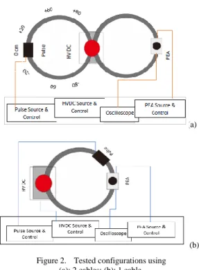
(b) Figure 2. Tested configurations using
(a): 2 cables; (b): 1 cable.
Figure 3. Rough PEA signals at applied voltages of ±5 kV and ± 3 kV. X-axis: 1000 points correspond to 800 ns with the sampling rate of 1.25 Gs/s used. Dotted lines represent the responses from the capacitive charge
peaks (left: outer semicon, right: inner semicon).
Figure 4. Peak to peak voltage comparison at +5 kV and varying impulse injector position. 0 500 1000 1500 2000 -6 -4 -2 0 2 4 -5kV -3kV +3kV +5kV P E A s ig n a l (10 -4 V ) Points -100 -80 -60 -40 -20 0 20 40 60 80 100 0.0 0.2 0.4 0.6 0.8 1.0 P -P S ig n a l A m p li tu d e ( m V ) Position (cm) Outer Inner
Figure 1. Schematic representation of the PEA Cable set-up
The arrangement shown in Fig. 1 provides good reliability when working with MV cables, 4.5 mm thick insulation, up to 100 kV. For miniature cables, the part of the semiconductor being removed brings fragility to the cable, and breakdown could occur at about 50 kV. A new way of making measurements was with the introduction of a second loop of cable [12] for applying the pulse. Then voltage as high as 90 kV could be applied with appropriate treatment of the terminations. The measurement results appeared however somewhat degraded in respect to previous achievements and our objective in the present work is to investigate in some detail the impact of the arrangement and optimize it.
Two configurations were tested to obtain an optimal signal. The first configuration uses two cables, see Fig. 2a, where the PEA module and the impulse voltage injector are on different cables. The second configuration is measurement using a single cable. PEA modules and impulse voltage injectors are placed on the cable under test (see Fig. 2.b). It is important to note that here the semicon was not removed between excitation point and detection point. It is anticipated that these arrangements deteriorate the quality of the acoustic signal. In the first case, the distance between excitation and detection and possible impedance mismatch can be the reason. In the second case, the result may depend on the high frequency impedance of the outer semicon, which could not be measured. For comparison purpose, in each configuration, a test is performed by varying the impulse voltage, the location of the PEA module and the DC voltage on the cable.
All the cables used in these tests have a length of about 3 m. Tests were realized using a pulsed generator of 30 ns duration, at a frequency of 1.5 kHz, using pulse amplitude of 0.4 kV or 1 kV. In the optimization step, we resorted to the calibration signal obtained under DC voltages of ±3 kV or ±5 kV. Then, in a second part some space charge results are shown. They were obtained at room temperature for voltages up to 35 kV, as well as under a temperature gradient of about 4°C applied by injecting a current in the cable conductor.
III. TEST RESULTS FOR DIFFERENT CONFIGURATIONS
A. Configuration with two cables
Fig. 3 shows the rough PEA signals obtained for a pulse voltage of 1 kV and for applied voltages varying from -5 kV to +5 kV. The acoustic response under 0 V dc voltage was subtracted to remove blank response and possible response from residual charges. The pulse injector was at position 0 cm in Fig. 2a. The response associated to the interface charges appears as a double peak for both the interface between insulation and outer screen (left) and with inner screen (right). The time lag between the first positive peak to the left and the first negative peak to the right (for applied voltage of 5 kV), considered as the positions of the electrode interfaces, is 655 ns. Considering a sound velocity for XLPE of 2200 m/s, this gives an insulation thickness of 1.45 mm, consistent with the mini-cable design. The response is roughly symmetrical with changing the polarity. There are oscillations of the signal (in-between the main peaks and beyond it) that appear related to the shape of the main peaks: it seems therefore to correspond to multiple reflections in the test bench and not to external noise linked for example to the pulse generator.
We now consider test realised at a fixed DC voltage of +5 kV, still with +1 kV impulse voltage, and investigate the effect of shifting the position of the PEA module. Positions
to the right and to the left of the middle point of the cable used for pulse application as far as 20 cm, 60 cm and 80 cm are considered. Fig. 4 shows the amplitude of the response at inner and outer semicon as a function of the position. We do not see strong variation in the amplitudes, being about 12% to the maximum.
When the pulse injector and PEA cell are not placed symmetrically on the loops, there can be some time lag appearing between excitation and detection depending on the route considered for electric pulse propagation. Considering a relative permittivity of 2.2, the pulse velocity in the cable is
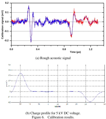
(a) Rough acoustic signal
(b) Charge profile for 5 kV DC voltage. Figure 6. Calibration results.
0.0 0.4 0.8 1.2 -0.2 -0.1 0.0 0.1 0.2 C a li b ra ti o n s ig n a l (m V ) Time (µs)
Figure 7. Space charge (a) and field (b) distributions for applied voltages of +/- 20, 25 and 35kV for 1 h at room temperature.
(a) (b) 35kV 25kV 20kV -20kV -25kV -35kV 35kV 25kV 20kV -20kV -25kV -35kV
of the order 0.15 m/ns. The propagation time for the voltage pulse is therefore of the order of 6 ns per meter, which is still small in respect to the propagation time of acoustic waves in the sample (x 100). Therefore, it is reasonable to detect mild effects as far the length difference remains of the order of 1 m, and the pulse absorption by the cable is small (the later was not evaluated). However, because of impedance mismatch, there can be harmonic voltages that produce delayed acoustic waves and hence some spurious peaks. The highest signal amplitudes in both the outer and inner interface response signals are obtained when the impulse injector module is located at -60 cm (counter-clockwise) from the middle of the loop.
B. Configuration with one cable
Fig. 5 shows the rough signals obtained in the configuration with one single cable, voltage conditions being the same as above. The distance between the pulse injector and the PEA module was 30 cm, see Fig. 2b. Comparatively to the previous response (Fig. 3), the peak-to-peak amplitude is substantially reduced, by a factor of more than 2. Changing the position on the same loop increased slightly the amplitude, without reaching that of the first arrangement.
Besides, the oscillations in the signal remain important and no improvement seems reached. For this reason, we conclude that the first configuration using two cable loops is much more suited. An advantage of this method is that the pulse connector is permanently maintained, providing better reproducibility of the results when changing cable sample for example.
IV. SPACE CHARGE RESULTS
A. Calibration
The calibration of the signal was achieved following the procedure described in [13] in which attenuation and dispersion of acoustic waves are taken into account. Fig. 6a depicts the rough calibration signal and that reconstructed taking into account the transfer function for acoustic waves through the insulation as well as the geometric factor for the cable. Results correspond to a DC field of 5 kV and a pulse voltage of 400 V. The charge profile of Fig. 6b obtained from the calibration signal provides an idea of the spatial resolution (which could be improved by lowering the smoothing of the output).
B. Space charge and field at room temperature
First tests were carried following a protocol in which voltage steps at –20 kV, +20 kV, -25 kV, +25 kV, -35 kV, +35 kV were applied successively for 1 h each. The applied
pulse voltage was 0.4 kV, at a frequency of 1.5 kHz. Space charges were acquired about every 6 min along the protocol.
Fig. 7.a shows the space charge distributions obtained during the all cycle. The profiles are very similar in shape, and appear symmetrical when changing the polarity. A small amount of charges is present in the middle of the cable and near the inner semicon, which changes sign with changing polarity. The response could be the consequence of some conductivity gradient along the radius.
The charge amounts are small, linked to the fact that the applied stresses are moderate, stressing time relatively short and measurements are at room temperature. In addition, the tested cables have been stored for several years in ambient conditions in such a way that crosslinking by-products that
Figure 5. Response to different voltage levels when positioning impulse injector at 30 cm from the PEA module on a single cable.
0 500 1000 1500 2000 -2 0 2 -5kV -3kV +3kV +5kV P E A s ig n a l (10 -4 V ) Points
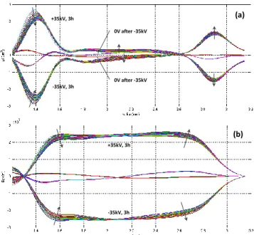
Figure 8. Space charge (a) and field (b) distributions for a cycle of -35kV (3h) / 0V (1h) / +35 kV (3h) / 0V (1h) under thermal gradient of
4°C in the insulation. +35kV, 3h -35kV, 3h -35kV, 3h +35kV, 3h 0V after -35kV 0V after -35kV (a) (b)
could stay as residues in the cable have been evacuated during storage.
Fig. 7b shows the distribution of electric fields in the cable. The field grossly follows a capacitive distribution vs. radius, i.e. it is about twice at the inner semicon compared to the outer semicon. A capacitive distribution is obtained under DC under the condition that conductivity is homogeneous (not dependent on the radius, therefore not dependent on the field) and that no space charge accumulates in the insulation.
C. Space charge and field under temperature gradient
In order to produce more significant amounts of charge, measurements were achieved while injecting a current in the conductor. With a current of 32 A, we have estimated that the temperature drop along the insulation of the cable was about 4°C. As the PEA cell acts a heat sink [12], the temperature at the measurement point was low, being about 30°C at the outer screen and 26°C at the inner screen.
The stress cycle consisted here in 3 h under -35 kV followed by one hour in volt-off. Then, the cycle was repeated for positive polarity. Fig. 8 shows the obtained results. Profiles do not appear as symmetrical as previously. There is a clear evolution in the charge pattern as a function of stressing time. The influence charge at the inner interface decreases in time while that at the outer interface increases. This corresponds to the field redistribution observed in Fig. 8b, leading to a nearly homogeneous field after 3 h charging. The evolutions found here seem to correspond mainly to a smoothing of the field by the conductivity gradient imposed by heating the cable: the field is moved to the cold part of the cable and a homocharge viewed from the hotter electrode develops in the bulk of the insulation. The residual space charge (at V=0) is somewhat larger after positive voltage application than negative one and this is reflected in the shape of residual field profile. Consistent results are therefore obtained under the moderate field applied in the present results.
CONCLUSIONS
We have shown that using a second cable loop for applying voltage pulses in PEA experiments constitutes the best way for avoiding to remove the semicon in the middle part of the cable prior to PEA measurements. This is of particular importance in the perspective of space charge measurements in miniature cables under high field in which weak point of the cable occurs after peeling the semicon.
Some space charge and field distributions results were presented with polarity reversal under moderate field, at room temperature and under thermal gradient. The material behavior appears mostly governed by conductivity gradient due to non-homogenous field and/or temperature, which appears consistent with the fact that cables were practically free from crosslinking by-products after long storage in ambient conditions. More work is to be achieved regarding the higher field behavior.
REFERENCES
[1] D. Fabiani, G.C. Montanari, C. Laurent, G. Teyssedre, P.H.F. Morshuis, R. Bodega, L.A. Dissado, A. Campus, and U.H. Nilsson, "Polymeric HVDC cable design and space charge accumulation. Part 1: insulation/semicon interface," IEEE Electr. Insul. Mag., vol. 23, n°6, pp. 11-19, 2007.
[2] D. Fabiani, G.C. Montanari, C. Laurent, G. Teyssedre, P.H.F. Morshuis, R. Bodega, and L.A. Dissado, "Polymeric HVDC cable
design and space charge accumulation. Part 3: Effect of temperature gradient," IEEE Electr. Insul. Mag., vol. 24, n°2, pp. 5-14, 2008. [3] H. Ghorbani, A. Abbasi, M. Jeroense, A. Gustafsson and M. Saltzer,
"Electrical characterization of extruded DC cable insulation — The challenge of scaling," IEEE Trans. Dielectr. Electr. Insul., vol. 24, pp. 1465-1475, 2017.
[4] N. Adi, T.T.N. Vu, G. Teyssèdre, F. Baudoin, N. Sinisuka, "DC model cable under polarity inversion and thermal gradient: build-up of design-related space charge," Technologies, vol. 5, p. 46 (16p), 2017. [5] D. Charrier, Q. Eyssautier, G. Perego, C. Frohne, and M. Jarvid,
"Leakage current behaviors under high electric field in polymer minicables," Proc. 10th Internat. Conf. on Insulated Power Cables (JiCable), Versailles, France, Paper B1-3, 2019.
[6] K. Fukunaga, H. Miyata, M. Sugimori and T. Takada, "Measurement of charge distribution in the insulation of cables using pulsed electroacoustic method," IEEJ Trans. Fundam. Mater., vol. 110, pp. 647–648, 1990.
[7] N. Hozumi, T. Takeda, H. Suzuki, and T. Okamoto, "Space charge behavior in XLPE cable insulation under 0.2-1.2 MV/cm dc fields," IEEE Trans. Dielectr. Electr. Insul., vol. 5, pp. 82-90, 1998.
[8] Z. Cao, Y. Zhang, C. Guo, F. Zheng. Z. An; S. Holé, E. Yu, X. Zheng, Z. Zhu, and L. Zhang, "Space charge measurement system based on laser PWP method for the full-size long HVDC cable," 2018 Proc. Condition Monitoring and Diagnosis (CMD) Conference, Perth, WA, pp. 1-4, 2018.
[9] J. Castellon, P. Notingher, S. Agnel, A. Toureille, F. Brame, P. Mirebeau, and J. Matallana, "Electric field and space charge measurements in thick power cable insulation," IEEE Electr. Insul. Mag., vol. 25, no. 3, pp. 30-42, 2009.
[10] G. Rizzo, P. Romano, A. Imburgia, and G. Ala, "Review of the PEA method for space charge measurements on HVDC cables and mini-cables," Energies, vol. 12, p. 3512 (23pp), 2019.
[11] T.T.N. Vu, G. Teyssedre, B. Vissouvanadin, J.Y. Steven, and C. Laurent, "Transient space charge phenomena in HVDC model cables," Proc. 9th Internat. Conf. on Insulated Power Cables (Jicable), Versailles, France, Paper A10.5, 2015.
[12] L. Berquez, J. Cènes, G. Teyssedre, S. Le Roy, P. Hondaâ, V. Eriksson, M. Bailleul, W. Loyens, and C. Moreau, "Implementation of space charge measurement using the Pulsed Electro-Acoustic method during ageing of HVDC model cable," 48th Cigré Session, Paris, Aug. 2020. Paper D1_0838, pp. 1-11, 2020.
[13] B. Vissouvanadin, T.T.N. Vu, L. Berquez, S. Le Roy, G. Teyssèdre, and C. Laurent, "Deconvolution techniques for space charge recovery using pulsed electroacoustic method in coaxial geometry," IEEE Trans. Dielectr. Electr. Insul. vol. 21, pp. 821-828, 2014.
![Fig. 1 depicts a very standard way used previously to probe space charges in model cables by PEA [11]](https://thumb-eu.123doks.com/thumbv2/123doknet/14373916.504794/2.893.485.804.906.1166/depicts-standard-previously-probe-space-charges-model-cables.webp)