HAL Id: hal-01821482
https://hal.sorbonne-universite.fr/hal-01821482
Submitted on 22 Jun 2018
HAL is a multi-disciplinary open access
archive for the deposit and dissemination of
sci-entific research documents, whether they are
pub-lished or not. The documents may come from
teaching and research institutions in France or
abroad, or from public or private research centers.
L’archive ouverte pluridisciplinaire HAL, est
destinée au dépôt et à la diffusion de documents
scientifiques de niveau recherche, publiés ou non,
émanant des établissements d’enseignement et de
recherche français ou étrangers, des laboratoires
publics ou privés.
Influence of water diffusion in deposited silicon oxides
on direct bonding of hydrophilic surfaces
J. Desomberg, Frank Fournel, Hubert Moriceau, A. Roule, E. Barthel, F.
Rieutord
To cite this version:
J. Desomberg, Frank Fournel, Hubert Moriceau, A. Roule, E. Barthel, et al.. Influence of water
diffu-sion in deposited silicon oxides on direct bonding of hydrophilic surfaces. Microsystem Technologies,
Springer Verlag, 2018, 24 (1), pp.801-808. �10.1007/s00542-017-3527-1�. �hal-01821482�
Influence of water diffusion in deposited silicon oxides on direct bonding of hydrophilic surfaces
J. Desomberg,1 F. Fournel,1 H. Moriceau,1 A. Roule,1 E. Barthel,2 and F. Rieutord3
1Univ. Grenoble Alpes, F-38000 Grenoble France. CEA, LETI, MINATEC Campus, F-38054, Grenoble, France 2SIMM – CNRS/ESPCI/UPMC, 10 rue Vauquelin 75005 Paris, France
3Univ. Grenoble Alpes, F-38000 Grenoble France. CEA, INAC, SP2M/NRS, F-38054, Grenoble, France Abstract
Direct bonding of PECVD SiOx films is of great interest in the field of microtechnologies for applications such as
stacked structures, thin film transfers, whose fabrication processes still deserve to be investigated.
This work deals with the influence of water diffusion in the SiOx films deposited onto 200mm Si wafers and its
impact on adherence of hydrophilic surfaces. The as-deposited film nature induces various stresses. Stresses evolutions and water penetration are characterized and a correlation is made between the kinetics of both stress variations and water diffusion through the oxide thin films. Impacts of room temperature (RT) storage prior to bonding and thermal treatments applied for strengthening the bonding is shown.
As direct bonding operates through surface asperities deformation, specific mechanical properties of such contact asperities can lead to a stronger bonding by increasing bonding area (Fournel 2015, Rieutord 2006; Ventosa 2008; Ventosa 2009). As the mechanical properties of silicon oxide material are greatly influenced by internal water concentration, aging and water diffusion on asperity have a real impact in term of direct bonding energy. Moreover at bonding interfaces, it is observed by X-ray reflectivity (XRR) that aging of deposited SiOx prior to bonding
enables shallower bonding gaps, indicating better bonding interface closure which is coherent with the bonding energy enhancement.
All these results confirm the link between water diffusion and hydrophilic surface adherence of deposited SiOx
films.
Introduction
Direct wafer bonding is a technique which consists in bringing into contact two mirror-polished wafers which are subsequently spontaneously held together by van der Waals forces at room temperature without addition of any polymer coupling material between the surfaces. This technique is more and more used in microelectronic applications such as film transfer, 3D integration and MEMS heterostructure assembly. A large distribution of insulator materials can be used in microelectronic fields but silicon dioxide material still remains widely used nowadays. As-deposited silicon oxides could be processed at low temperature and the sealing of the bonding interface could also be done at low temperature to allow some new applications for direct bonding of insulator materials. Direct bonding of thermal silicon dioxides was widely investigated for the last decade, but deposited silicon oxides direct bonding stills deserve to be investigated.
In this way Plasma-Enhanced Chemical Vapor Depostion (PECVD) silicon oxides (SiOx, x lower or equal to 2) is
investigated for direct bonding. Main challenges in this study consist in getting an efficient bonding of deposited silicon oxides in terms of both bonding energy and defects density within the temperature range [RT-500°C] and in developing a better understanding of phenomena involved in direct bonding of deposited silicon oxides. Especially, the main objective is to understand the influence of trapped species in deposited silicon oxide thin films. Our investigation is focused on the water influence in those thin films. The nature of these deposited films is also investigated. This nature which depends on deposition parameters and post-deposition preparation has a great impact on the water absorption kinetic throughout the oxide films. Then the internal water concentration could be tuned and could have an impact on the mechanical or physicochemical surface properties of those films. These property modifications are shown to have a strong impact on wafer direct bonding of deposited silicon oxides. Deposited silicon oxides bonding strength dependence on various parameters are reported here.
Experiments
This study is carried out on 200 mm, lightly p-doped Si(100) wafers. Two kind of PECVD silicon oxides are deposited at 400°C on these wafers with tetraethyl orthosilicate (TEOS) precursor depending on the injection system: one is based on liquid direct injection and the other one uses a bubbler injection. Different thicknesses
from 150 nm to 1 µm are deposited. It will allow having a better understanding of the trapped species density influence in these films for bonding applications.
After the film deposition these wafers are submitted to different treatments prior bonding. For instance a thermal treatment (450°C, 2 hours under O2) is applied after deposition on a few samples in order to study a silicon oxide
drying step prior bonding. Many films are stored at RT in cleanroom environment with 45% of relative humidity (RH) to see the aging influence. Chemical Mechanical Polishing (CMP) is then performed (50 nm removed) in order to reach the needed roughness for direct bonding at room temperature and to enhance hydrophilic behavior of silicon oxide films just before the bonding in cleanroom. The sample behaviors are investigated after various thermal treatments in the [RT-500°C] range for 2 hours allowing the partial sealing of the bonding interface. Many characterizations are done on the thin films (prior bonding and CMP) such as stress measurements over time (with RT storage in cleanroom environment at 45%RH). These stress measurements are done by an optical interferometer which measure the bow before and after deposition and give us the residual stress. From the difference of wafer curvature radius before and after deposition, the stress is calculated thanks to the Stoney formula. In addition, the film chemical compositions are given by Fourier Transform Infrared (FTIR) spectroscopy in transmission mode. This allows an aging monitoring by moisture absorption characterization.
Once bonding are annealed at various temperature in the [RT-500°C] range, bonding energy, defect density and bonding interface closure are investigated. The bonding energy is measured by the double cantilever beam (DCB) technic under prescribed load on 2 cm wide strip samples, which consists in a razor blade insertion at the bonding interface and the induced debonded length measurement. The measurement are done in anhydrous atmosphere to avoid any external water stress corrosion. The bonding energy G is calculated with the debonded length using the following El-Zein equation
𝐺 =16.𝛽3.𝛿2.𝑡3 11.𝑎4 . 1 1−𝑡3.𝛽26 8.𝛽11.𝑎4 with 𝛽𝑖𝑗 = 𝑆𝑖𝑗 𝑆𝑖3.𝑆𝑗3 𝑆33 ,
Where a is the debonded length, t the wafer thickness, δ the inserted blade thickness, and Sij the general term of
compliance tensor in the opening direction (El-Zein 1988) in order to take into account the silicon anisotropy (Fournel 2012). The defect density is investigated by acoustic microscopy. Otherwise high energy interfacial x-ray reflectivity (XRR) which gives the electron density profile of the bonding interface is used to get a better understanding of bonding closure mechanisms.
Results and discussion
In this paper, a global investigation of deposited silicon oxides films evolution over the aging time is done and it impacts on direct bonding are reported here. In a first part, the influence of the material nature and the aging duration on the water amount inside those thin films and its impact on direct bonding is shown. This is highlighted by high energy XRR results to characterize the bonding interface sealing. In a second part, a link is demonstrated between residual stresses kinetic evolutions of deposited silicon oxides thin films and water absorption kinetic evolution. In a third part, the impact of deposited silicon oxide thickness on water absorption and its impact on direct bonding is investigated. Finally some additional investigations were done concerning stress variation in order to go more deeply into this absorption phenomenon.
Contrary to thermal silicon oxides which are structurally well defined overall their thickness, PECVD silicon oxides may have various nature of material depending on the nature of the technical deposition, the RF power chosen, the O2/TEOS ratio flow chosen (Sabbione 2012) or other technical deposition parameters such as the
deposition temperature. Moreover PECVD silicon oxides may have an evolution of their intrinsic structure in thickness. All these parameters which could be tuned for deposited silicon oxides may have a great impact on the moisture absorption. This moisture absorption capability of deposited silicon oxides have a significant impact on direct bonding energy as higher values could be reached (above 5 J/m² in the post-bonding annealing temperature [200°C-500°C] range) with them compared to the thermal silicon oxides (bonding energy from 0.8 J/m² to 5 J/m² in the post-bonding annealing temperature [200°C-500°C] range) (Fournel 2012).
In order to investigate the material nature influence in the case of PECVD silicon oxides, the capability of two different films to absorb moisture over the time is studied. Different kinds of TEOS injection systems are chosen such as Liquid direct injection in which TEOS injection debit in the reactor is accurately controlled or Bubbler injection in which TEOS injection debit is depending on the saturated vapor pressure.
FTIR measurements are performed on those two materials (1 µm deposited here on Si bulk) at different time after silicon oxide deposition in order to get the time evolution of the -OH and H2O absorption band. The FTIR spectra
i.e. the wavenumber dependence in the [3000 cm-1-3800 cm-1] range of the absorption coefficient of both materials
is plotted in Figure 1. FTIR spectra of all deposited films show the presence of isolated Si-OH groups vibrating at 3650 cm-1. Regarding the as-deposited films, both PECVD silicon oxides thin films have a certain capability to
absorb moisture just after deposition as demonstrated here by the detection of a broad absorption band around 3300-3400 cm-1 which can be assigned to the associated Si-OH bonds and free H
2O. All aged thin films were
stored 2 months in cleanroom environment at a monitored 40% room humidity (RH). Noteworthy, the bubbler injection silicon oxide thin film (red curve for the as-deposited material and pink curve for the aged material) has a higher propensity to absorb moisture over the time than liquid direct injection silicon oxide thin film (black curve for the as-deposited material and grey curve for the aged material). A huge behavior difference regarding the moisture absorption could then be seen just by changing the PECVD injection type.
Moreover, even just after the deposition the bubbler injection silicon oxide thin films has a higher absorption bands in the 3300-3400 cm-1 range than both 2 months aged and as-deposited liquid direct injection materials. It
emphasizes again the difference of those two materials in their intrinsic nature and composition. This should have an impact in terms of physicochemical and mechanical parameters of these oxides surfaces and sub-surfaces and should impact the sealing of the bonding interface and then the direct bonding energy.
Moreover the 2 months aged bubbler injection thin films a higher amount of isolated Si-OH groups (3650 cm-1)
than all other materials (aged and as deposited liquid direct injection materials and as deposited bubbler injection material). These isolated Si-OH groups are probably located at the surface of the silicon oxides and should then have a great impact on subsurfaces physicochemical properties and on direct bonding. This effect will not be studied in this work as a CMP step which remove roughly 50 nm of material is performed just before the bonding. This process allows a reduction of the root mean squared (RMS) roughness and have a chemical action on the surface and the subsurface which facilitates direct hydrophilic direct bonding. First of all, as shown on Figure 2, the direct bonding energies of symmetrical as deposited liquid direct injection bonding and as deposited bubbler injection bonding are measured regarding different post bonding annealing temperature.
Above 200°C, the direct bonding energy of the as-deposited bubbler injection silicon oxide bonding is higher than the corresponding bonding energy of the liquid direct injection silicon oxide bonding. This is due to a difference in terms of global material structure. Indeed as previously shown, FTIR spectra of as-deposited bubbler injection materials got a higher amount Si-OH and H2O than the as-deposited liquid direct injection materials. Moreover,
an outstanding increase of direct bonding energy between 100°C and 200°C can be seen for bubbler injection material. This thin film has absorbed a certain amount of water and this water is used to improve the sealing of the bonding interface. As demonstrated later in Figure 11 and 12, 200°C is needed to allow this water to be used at the bonding interface to strengthen it.
Finally as-deposited bubbler injection bonding has a bonding energy at 500°C far above 5 J/m2 which is known to
be the energy silicon fracture. As the sample aren’t broken during the blade insertion and the sample was opened at the bonding interface it proves that a little amount of energy is lost throughout the silicon oxide volume. The system is not purely elastic.
In order to understand more deeply some mechanisms involved in the sealing of the bonding interface for PECVD SiO2 thin films depending of ageing and deposited silicon oxide thickness some additional investigations were
performed. Some bonding were characterized by high energy XRR. This experimentation allow to measure the gap profile of the bonding interface. The gap profile of these bonding depending on the post-bonding annealing temperature is plotted in Figure 3. It appears that as-deposited PECVD SiO2 bonding have a higher gap profile at
the bonding interface rather than aged PECVD SiO2 thin films, even at room temperature. This underline the
impact of aging prior bonding for those deposited films, even at room temperature which means there is a physicochemical impact on the silicon oxide surface of aging. Aging allow a better closure of the bonding interface which means a higher bonding area. For aged thin films a high decrease of gap profile operates between 200°C and 300°C which correspond to a motion of water from the silicon oxide volume to the bonding interface. This is demonstrated later in Figure 11 and 12. Moreover 100 nm as-deposited PECVD liquid direct injection bonding have a lower gap profile than 1 µm as-deposited PECVD liquid direct injection bonding. This will confirm following results (Figure 6) related to bonding energy of thinner thin films.
It is then demonstrated that deposited silicon oxides thin films are able to absorb moisture depending on their deposition technic (bubbler or liquid injection) and it seems that this absorbed water have an impact on the sealing of the bonding interface. Then it appears interesting to investigate more deeply the influence of aging in those thin films. For this purpose, the time dependence of the stress variation in those films is measured. As shown on Figure 4, there is an important difference between the two material deposition types.
Bubbler injection silicon oxide is tensile with a residual stress of 40 MPa just after deposition and become more and more compressive over the time. On the other side liquid direct injection silicon oxide is compressive just after deposition with a residual stress around -70 MPa and become a little more compressive over the time but its dynamic is much smaller than the bubbler injection one. Moreover, after 65 days, the bubbler stress is even lower than the liquid one. There is then a strong correlation between the kinetic of stress variation of PECVD SiO2 thin
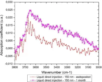
films and the kinetic of water diffusion shown by the FTIR spectra. Various stress variation kinetics induces various water absorption kinetics. Because of its tensile stress as deposited bubbler material have an ability to facilitate the water absorption and become more and more compressive as a result of water penetration inside. In order to see the impact of the silicon oxide deposited thickness on water absorption and on direct bonding, a 150 nm bubbler material is compared to the 1 µm thin film.
As shown on Figure 5, there is a higher kinetic of stress variation concerning the thinner film compared to the thicker one. This means that thinner bubbler injection materials have a better capability to absorb moisture to the thicker one and this may have an impact on direct bonding energy. Indeed as shown on Figure 6, the symmetrical direct bonding energy of both material thickness exhibit quite different values even with as deposited films. As-deposited 100 nm bubbler materials exhibits a very high bonding energy close to 7 J/m² with a 400°C post-bonding annealing compared to 1 µm as-deposited one which has a bonding energy close to only 5 J/m² with the same post-bonding annealing temperature. This results concerning the better post-bonding energy of thinner films is confirmed by XRR measurements which have shown that thinner films bonding have a lower gap profile at the bonding interface. The same thickness impact is also observed for the liquid injection material. The residual stress variation over the time of a 150 nm PECVD SiO2 thin film obtained by liquid direct injection compared to a the residual stress
variation over the time of a 1 µm PECVD SiO2 thin film obtained by liquid direct injection is plotted in Figure 7.
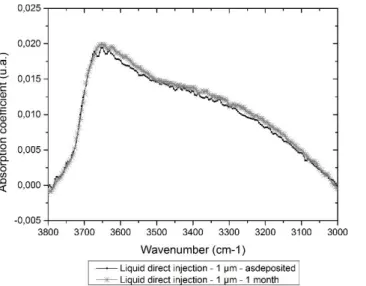
As seen in Figure 7, both PECVD SiO2 thin films thick (1 µm) and thin (150 nm) have a residual stress just after
deposition close to -80 MPa. This is normal as this value depends only on the nature of the material and on the deposition parameters. However both films haven’t the same stress variation kinetic over the time. While 1 µm thin film have a slight decrease of residual stress over the time the 150 nm thin film have a huge decrease of residual stress over the time which means that this film is able to absorb moisture quite quickly. In order to confirm this assumption, these thin films undergo FTIR measurements. The evolution in time of –OH and H2O absorption
bands of a 1 µm PECVD SiO2 thin film obtained by liquid direct injection is plotted in Figure 8. In the same way
corresponding evolution in time of –OH and H2O absorptions bands of a 150 nm PECVD SiO2 thin film obtained
by liquid direct injection is plotted in Figure 9. As seen before thin films with a high kinetic variation of residual stress have also a high capability to absorb moisture as observed here for this 150 nm PECVD thin film rather than 1 µm one.
It is then very interesting to note that a very thin thickness enhance the water absorption kinetics. This allows us to produce direct bonding structure with important bonding energy even with the liquid direct injection material. After a CMP step, wafer bonding is operated with a as-deposited and a 2 months aged 150 nm thin film The evolution of the direct bonding energy is plotted on Figure 10.
Aged 150 nm liquid direct injection silicon oxide bonding shows a bonding energy of 7.5 J/m2 after a bonding consolidation at 400°C during two hours against only 5.5 J/m2 for it corresponding as deposited material. This results emphases the significant role of water in the proceeds of the bonding interface sealing. It seems there is an impact of water since room temperature and this effect is increased above 200°C. The reason of this increased bonding energy is either due to a better concentration of Si-OH group at bonding interface which increase the dangling bonds density at the surfaces or due to some mechanical properties of those thin films which has been impacted by a high concentration of water in the subsurface allowing a higher bonding area during bonding consolidation.
It is then demonstrated that water diffusion in PECVD oxide film is quite interesting for direct bonding energy. In order to go more deeply into this absorption phenomenon, some additional investigations are done concerning
stress variation. An aged bubbler injection silicon oxide is investigated and undergoes two in-situ subsequent stress variation measurements versus temperature from room temperature to 500°C and backward. Two sequential thermal cycle are done during the same experiment under nitrogen atmosphere. These two in-situ subsequent stress variation measurements versus temperature are plotted in Figure 11.
As shown on Figure 11 the aged thin film has an initial residual stress of -150 MPa and this thin film become less and less compressive with the increase of temperature. From 200°C to 500°C water desorption operates. After this increase of temperature, the sample is cooling down until room temperature and get the standard residual as deposited stress (cf. Figure 4). An additional thermal cycle is done and the residual stress variation correspond to the silicon oxide coefficient of thermal expansion (CTE) difference with the silicon wafer one which means without any water impact.
Corresponding measurements of –OH and H2O absorption bands after deposition, 3 months after deposition and
after first and second thermal cycle are plotted in Figure 12.
As shown on Figure 12, after a first thermal cycle there is no longer water inside the thin film which is coherent with a residual stress back to the initial stress measured just after deposition as shown on Figure 11. However, after those thermal treatments the silicon oxide films are again able to absorb moisture. The residual stress variation over the time of PECVD SiO2 thin films without thermal cycle and after two thermal cycles is plotted in Figure
13.
After water "drying", PECVD silicon oxides thin films has a residual stress variation over the time which follow almost the initial residual stress variation after deposition. As proved before a similar kinetic of stress variation means a similar kinetic of water absorption over the time.
Conclusion
A global investigation of PECVD silicon oxide thin films is made in order to see the impact of intrinsic properties of those thin films on direct bonding. It is shown that deposited silicon oxides have various deposition parameters which can be tuned. Depending on these deposition parameters and how these parameters are tuned various kinetic of residual of stress variations could be induced. It is demonstrated a special relationship between the stress variation kinetic over the time with the water absorption kinetic which have a significant impact on direct bonding. Water management inside deposited silicon oxide is then a key point to improve direct bonding of these oxides. Water induces special mechanical or physicochemical properties on asperities in contact at the bonding interface which can increase the bonding energy. Water could reduce the stiffness of asperities in contact at the bonding interface and increase the bonding area.
Acknowledgments
This work was funded by the Commissariat à l'Energie Atomique et aux Energies Alternatives (CEA) of Grenoble.
References
El-Zein M, Reifsnider K (1988) Evaluation of GIC of a DCB specimen using an anisotropic solution. Journal of
Composites, Technology and Research, Vol. 10, No. 4, pp. 151-155. doi: 10.1520/CTR10278J
Fournel F, Continni L, Morales C, Da Fonseca J, Moriceau H, Rieutord F, Barthelemy A, Radu I (2012) Measurement of bonding energy in an anhydrous nitrogen atmosphere and its application to silicon direct bonding technology. Journal of Applied Physics 111, 104907. doi: 10.1063/1.4716030
Fournel F, Martin-Cocher C, Radisson D, Larrey V, Beche E, Morales C, Delean PA, Rieutord F, Moriceau H (2015) Water stress corrosion in bonded structures. ECS Journal of Solid State Science and Technology, 4(5) p124-p130. doi: 10.1149/2.0031505
Rieutord F, Capello L, Beneyton R, Morales C, Charvet AM, Moriceau H (2006) Rough surface adhesion mechanisms for wafer bonding. ECS Transaction, 3 (6) 205-215. doi: 10.1149/1.2357071
Sabbione C, Di Cioccio L, Vandroux L, Nieto JP, Rieutord F (2012) Low temperature direct bonding mechanisms of tetraethyl orthosilicate based silicon oxide films deposited by plasma enhanced chemical vapor deposition. Journal of Applied Physics 112, 063501. doi: 10.1063/1.4752258
Ventosa C, Rieutord F, Libralesso L, Morales C, Fournel F, Moriceau H (2008) Hydrophilic low temperature direct wafer bonding. Journal of Applied Physics 104, 123524. doi: 10.1063/1.3040701
Ventosa C, Morales C, Libralesso L, Fournel F, Papon AM, Lafond D, Moriceau H, Penot JD Rieutord F (2009) Mechanism of thermal silicon oxide direct wafer bonding. Electrochemical and Solid-State Letters, 12 (10) H373-375. doi: 10.1149/1.3193533
Figure Captions :
Figure 1 : Time evolution of the -OH and H2O band observed by FTIR for different natures of thin films and aging
duration after deposition ... 8 Figure 2 : Direct bonding energy evolution regarding the post bonding annealing temperature of as-deposited PECVD thin films. ... 8 Figure 3 : Gap Profile of bonding interface of various as-deposited and aged PECVD SiO2 bonding regarding
post-bonding consolidation temperature ... 9 Figure 4 : Residual stress variation over the time of different nature of PECVD thin films of SiO2 ... 9
Figure 5 : Residual stress variation over the time of a 150 nm and 1 µm PECVD SiO2 thin film obtained by bubbler
injection. ... 9 Figure 6 : Direct bonding energy evolution regarding the post bonding annealing temperature of bonded structures with as-deposited bubbler PECVD SiO2 thin films of various thicknesses ... 10
Figure 7 : Residual stress variation over the time of a 150 nm PECVD SiO2 thin film obtained by liquid direct
injection (red curve) and a 1 µm PECVD SiO2 thin film obtained by liquid direct injection (black curve) ... 10
Figure 8 : Evolution in time of -OH and H2O absorption bands of a 1µm PECVD SiO2 thin film obtained by liquid
direct injection... 10 Figure 9 : Evolution in time of -OH and H2O absorption bands of a 150 nm PECVD SiO2 thin film obtained by
bubbler injection material ... 11 Figure 10 : Direct bonding energy regarding the post bonding annealing temperature with as-deposited and 2 months aged 150 nm PECVD SiO2 thin films ... 11
Figure 11 : Two in-situ subsequent stress variation measurement versus temperature from room temperature to 500°C and backward (thermal cycle) of a 3 months aged bubbler injection deposited SiO2 thin film. ... 11
Figure 12 : Measurement of -OH and H2O absorption bands observed by FTIR of a bubbler injection material after
deposition (black curve), 3 months after deposition (red) and after a first (blue) and second (purple) thermal cycle ... 12 Figure 13 : Residual stress variation over the time of PECVD SiO2 thin films without thermal cycle and after two
Figure 1 : Time evolution of the -OH and H2O band observed by FTIR for different natures of thin films and aging duration after deposition
Figure 2 : Direct bonding energy evolution regarding the post bonding annealing temperature of as-deposited PECVD thin films.
Figure 3 : Gap Profile of bonding interface of various as-deposited and aged PECVD SiO2 bonding regarding post-bonding consolidation temperature
Figure 4 : Residual stress variation over the time of different nature of PECVD thin films of SiO2
Figure 6 : Direct bonding energy evolution regarding the post bonding annealing temperature of bonded structures with as-deposited bubbler PECVD SiO2 thin films of various thicknesses
Figure 7 : Residual stress variation over the time of a 150 nm PECVD SiO2 thin film obtained by liquid direct injection (red curve) and a 1 µm PECVD SiO2 thin film obtained by liquid direct injection (black curve)
Figure 8 : Evolution in time of -OH and H2O absorption bands of a 1µm PECVD SiO2 thin film obtained by liquid direct injection
Figure 9 : Evolution in time of -OH and H2O absorption bands of a 150 nm PECVD SiO2 thin film obtained by bubbler injection material
Figure 10 : Direct bonding energy regarding the post bonding annealing temperature with as-deposited and 2 months aged 150 nm PECVD SiO2 thin films
Figure 11 : Two in-situ subsequent stress variation measurement versus temperature from room temperature to 500°C and backward (thermal cycle) of a 3 months aged bubbler injection deposited SiO2 thin film.
Figure 12 : Measurement of -OH and H2O absorption bands observed by FTIR of a bubbler injection material after deposition (black curve), 3 months after deposition (red) and after a first (blue) and second (purple) thermal cycle
Figure 13 : Residual stress variation over the time of PECVD SiO2 thin films without thermal cycle and after two thermal cycles