HAL Id: tel-01595959
https://tel.archives-ouvertes.fr/tel-01595959
Submitted on 27 Sep 2017
HAL is a multi-disciplinary open access archive for the deposit and dissemination of sci-entific research documents, whether they are pub-lished or not. The documents may come from teaching and research institutions in France or abroad, or from public or private research centers.
L’archive ouverte pluridisciplinaire HAL, est destinée au dépôt et à la diffusion de documents scientifiques de niveau recherche, publiés ou non, émanant des établissements d’enseignement et de recherche français ou étrangers, des laboratoires publics ou privés.
development of atomic-vapour photonic microcell
Ximeng Zheng
To cite this version:
Ximeng Zheng. Fiber post-processing and atomic spectroscopy for the development of atomic-vapour photonic microcell. Optics / Photonic. Université de Limoges, 2017. English. �NNT : 2017LIMO0031�. �tel-01595959�
Université de Limoges
École Doctorale Sciences et Ingénierie pour l’Information,
Mathématiques (ED 521)
Institute de recherche XLIM, UMR CNRS 7252, Limoges
Thèse pour obtenir le grade de
Docteur de l’Université de Limoges
Electronique des Hautes Fréquences, Photoniques et Systèmes
Présentée et soutenue par
M. Ximeng ZHENG
Le 18 juillet 2017
Thèse dirigée par Pr. Fetah BENABID et Dr. Frédéric GEROME
JURY :
Président du jury :
Mr. Philippe Thomas, Directeur de recherche, SPCTS, Centre Européen de la Céramique, Université de Limoges
Rapporteurs:
Mr. Patrick Windpassinger, Professeur, Universität Mainz
Mr. Daniel Bloch, Directeur de recherche CNRS, Laboratoire de Physique des Lasers, Université Paris13
Examinateurs :
Mr. Luca Vincetti, Professeur associé, Université de Modena
Mr. Simon Bernon, Maitre de conférence, Laboratoire Photonique, Numérique et Nanosciences, Institut d’Optique d'Aquitaine – Université Bordeaux 1
Mr. Fetah Benabid, Directeur de Recherche CNRS, XLIM, Université de Limoges Mr. Frédéric Gérôme, Chargé de Recherche CNRS, XLIM, Université de Limoges
Fiber post-processing and atomic spectroscopy for the
development of atomic-vapour photonic microcell
M. Ximeng ZHENG | Thèse de doctorat | Université de Limoges | I
Acknowledgement
I would like to thank my supervisor Pr. Fetah Benabid for give me the opportunity to complete my Ph.D research. Thank his expertise, support and guidance through these years. Without him, this wide topic thesis would not be accomplished. I would also like to thank my wife Sixia Liu, who gave me strong support in mental part during my hard Ph.D life. I would like to thank the past and present members of the Gas Phase Photonics and Microwave Materials Group. Specially thank Dr. Frédéric Gérôme for teach me the basic knowledge in these years and give me all neccesairy help. His kindness and French elegance will accompany me in my future research life. I would also like to thank Benoît Debord for the Kagome HC-PCF samples fabrication. Thank Jenny Juin and Thomas Philippe in laboratory SPCTS for the help of inner wall surface anti-relaxation material coating. Thank Luca Vincetti for the guidance simulation part. Thank kind Sébastien Rougier for teach me the fiber drawing and the SEM characterization. Additionally I would like to achnowledge our lab crews in Limoges: Benoît Beaudou, Assaad Baz, Meshaal Alharbi, Muhammed Adnan, Ekaterina Ilinova, Abhilash Amsanpally, Madhoussoudhana Dontabactouny, Aurélien Benoît, Katell Gadonna, Debashri Ghosh, Florien Vial, Amrani Foued, Matthieu Chafer, Maurel Martin, Kergoustin David, Delahaye Frederic.
M. Ximeng ZHENG | Thèse de doctorat | Université de Limoges | III
Un peuple malheureux fait les grands artistes. ˗ Alfred de MUSSET à mon grand-père
M. Ximeng ZHENG | Thèse de doctorat | Université de Limoges | i
Abstract
Atom optics in confined in nano- and micro-structured devices geometry is becoming a timely topic. The pursuit of miniaturizing atom based functionalities such as frequency references, atomic clocks and quantum sensors is motivated by transferring the outstanding performances in frequency control and coherent optics achieved in laboratory environments to a broader community of users through the development a compact, friendly-user and stand-alone atom devices. Moreover, atomic-vapor micro-confinement implies innovative technological solutions and platform to explore new fundamental phenomena.
Among the atom devices that have been or are being developed, we cite hollow-core photonic crystal fiber (HC-PCF) and its gas-filled form the photonic microcell (PMC). The latter outstands with its long interaction length and small modal area, making it thus an efficient platform to enhance gas-laser nonlinear interaction and/or absorption contrast by several orders of magnitude relative to free-space configurations. However, the micrometric scale of the fiber core harboring the atoms raises several technical and scientific challenges. Among the technical challenges, we list the development of efficient process for atom loading inside very long hollow channels with small core diameter, the suppression or mitigation of physio-chemical reactivity of the confined atoms (i.e. Rubidium, Caecium) with the fiber core inner-surface silica etc. In parallel, once the atoms are successfully confined, the large surface-to-volume ratio of the atom-harboring fiber-core raises questions like the coherence relaxation dynamics and the nature and effect of the atom-surface interaction. Within this context, the work presented in this thesis builds up on previous work in my research group GPPMM to address some of the above-mentioned challenges. In particular, the thesis reports on fiber-core inner surface coating with different materials as an effort to mitigate
M. Ximeng ZHENG | Thèse de doctorat | Université de Limoges | ii
the physio-chemical reactions of the confined atoms with the surface, on tapering large outer-diameter and core-diameter inhibited coupling guiding Kagome HC-PCF, and splicing technique that ensures low splice loss and no atomic reactivity during the splicing process. In parallel, the thesis reports on a set of spectroscopy experiments to assess the relaxation dynamics of atoms inside HC-PCF and to report on novel sub-Doppler transparencies.
The manuscript is structured as follows. Chapter 1 introduces the context of atom optics in micro-structured systems, the scientific and technological motivations behind this theme and review the different development and results achieved in the last two decades.
Chapter 2 details the description of guidance mechanism of the HC-PCF. We draw the main differences between photonic bandgap guiding HC-PCF and Inhibited-Coupling guiding HC-PCF. We list the main modal properties of IC guiding HC-PCF, which is used along this thesis, and the rationale behind the choice of this type of fibers for our atom-optics experiments and aim to develop all-fiber Rb-PMC. We then show the optical and physical properties of Kagome HC-PCF that are purposely fabricated to operate near 780 nm, and which will be used throughout my doctoral wotk.
In Chapter 3, we introduce the different processes in post-processing HC-PCF before, during and after the atom loading inside the fiber. This process chain is required in making what would be the first all-fiber alkali-vapor photonic microcell (PMC). It comprises HC-PCF tapering, splicing, in-fiber gas handling, fiber core inner-wall coating and of course vapor loading. The chapter stresses on techniques of tapering HC-PCF with hypocycloid core-contour with no structural distortion and splicing them to an all-solid optical fiber. The chapter presents also alternative ways to splice HC-PCF to solid fiber using sleeving techniques. Finally, we report on the coating material synthesis and on the process of the fiber core
M. Ximeng ZHENG | Thèse de doctorat | Université de Limoges | iii
inner-wall coating. Several HC-PCFs with ceramic and PDMS coated core along with uncoated HC-PCF have been put in a high vacuum system for rubidium loading, lifetime assessment and for spectroscopy experiments. The results show that all the coated HC-PCF kept their optical performances. As expected, the ceramic coated HC-PCFs exhibit much longer Rb life time inside the fiber which is paramount for stand-alone PMC applications.
Chapter 4 deals with investigating the atom dephasing dynamics inside the core with an emphasis on the effect of the surface. In this chapter, we present experimental results on the relaxation dynamic of rubidium ground state polarization relaxation. The experimental protocol relies on monitoring the magneto-optical rotation of the atoms in the dark. Based on this technique, relaxation time of Rb inside HC-PCF with different core inner-wall surfaces and under different magnetic field amplitude, pump power levels have been measured. The results demonstrate that the measured polarization relaxation is dominant by the dwell time of the adsorbed atoms and that the polarized atoms are primarily formed by slow atoms. Finally, we used this technique to deduce the dwell time for bare silica surface, ceramic coating and PDMS coating.
Chapter 5 introduces Rb-surface interaction induced sub-Doppler transparencies observed in the absorption spectrum of Rb-confined vapor inside a Kagome HC-PCF. Unlike with saturated absorption or electromagnetically induced transparency, the sub-Doppler lines are generated with a single forward propagating laser beam. The chapter reports on how these sub-Doppler transparencies change with magnetic field, laser power and polarization for three different core inner-wall surfaces. Then, the results are compared with those of a theoretical model, which considers the adsorbed atom trapped in a Van-der-Waal potential, and shows that sub-Doppler transparencies can occurs via optical pumping between the translational energy levels of the adatoms inside the potential. The comparison between the theoretical model and the experimental
M. Ximeng ZHENG | Thèse de doctorat | Université de Limoges | iv
results show a qualitative consistency and paves the way for a novel spectroscopy based on atoms in HC-PCF.
M. Ximeng ZHENG | Thèse de doctorat | Université de Limoges | v
Table of contents
Abstract ... ...错误!未定义书签。 Chapter 1 ... 1Atom optics in gas confined hollow-core photonic microstructures ... 1
1.1 Introduction ... 2
1.2 Basics of atom-light interaction... 4
Spectral line shapes ... 4
Coherence ... 8
Sub-Doppler transparencies generated techniques ... 10
1.3 Compact host for atomic optics ... 14
Compact quantum sensors in electronic structure: Chip Scale Atomic Clock (CSAC) and Chip Scale Atomic Magnetometer (CSAM) ... 15
Atom cell based on Hollow-Core Anti Resonant Reflecting Optical Waveguide (ARROW)... 17
Gas-cell based on Hollow-Core Photonic Crystal Fiber ... 17
Comparison of atom-confined photonic structures ... 18
1.4 Atom-Laser interaction enhancement in HC-PCF ... 19
1.5 Progress in Gas Filled HC-PCF ... 21
1.6 The dephasing effects in HC-PCF ... 22
1.7 Atom loading in HC-PCF ... 24
1.8 Summary and thesis outline ... 28
1.9 References... 30
Chapter 2 ... 41
Hollow-core photonic crystal fiber guidance ... 41
2.1 Introduction ... 42
2.2 Photonic Bandgap guidance HC-PCF ... 44
2.3 Photonic Tight Binding Model ... 46
2.4 Double Photonic Bandgap guidance mechanism ... 48
2.5 Inhibited Coupling Kagome lattice HC-PCF... 50 2.6 Enhanced Inhibited coupling hypocycloid core shape Kagome HC-PCF 52
M. Ximeng ZHENG | Thèse de doctorat | Université de Limoges | vi
2.7 PBG vs IC HC-PCFs for atomic applications at 780 nm ... 57
2.8 Properties of the HC-PCFs under test ... 58
Fiber selection for the post-processing work ... 59
Fiber selection for ground state atomic polarization relaxation time work... 60
Fiber selection for Sub-Doppler transparencies work ... 62
2.9 Summary ... 63
2.10 References ... 64
Chapter 3 ... 69
Post-processing of hollow-core photonic crystal fiber ... 69
3.1 Photonic microcells (PMCs) ... 70
3.2 IC-PMC vs PBG-PMC ... 70
3.3 Inhibited Coupling hypocycloid core Kagome fiber tapering... 72
3.4 Inhibited Coupling hypocycloid core Kagome fiber splicing ... 78
3.5 Inhibited coupling hypocycloid core Kagome fiber sleeve ... 80
3.6 Anti-relaxation material inner wall surface coating ... 83
Polydimethylsiloxane (PDMS) solution synthesis ... 83
Aluminosilicate Sol-Gel solution synthesis ... 84
HC-PCF preparation and coating procedure ... 85
Optimization of the Aluminosilicate Sol-Gel coating ... 87
3.7 Rubidium vapor in sol-gel and PDMS coated Kagome HC-PCF ... 92
The challenges of reactive alkali atom loading in micrometric HC-PCF... 93
Discussion of anti-relaxation materials inner surface coating for alkali metal vapors applications ... 93
Rubidium vapor lifetime in sol-gel coated Kagome HC-PCF ... 95
The loading atomic density in Rb-filled HC-PCFs ... 97
3.8 Summary ... 99
3.9 References... 100
Chapter 4 ... 107
Ground-state atomic polarization relaxation measurements in Rb filled HC-PCF with different core inner-surfaces ... 107
4.1 Introduction ... 108
M. Ximeng ZHENG | Thèse de doctorat | Université de Limoges | vii
4.3 Ground state atomic polarization relaxation time measurement experimental set-up ... 112
Experimental set-up and atomic polarization relaxation measurement ... 112
Transit time and dwell time deduction ... 118
4.4 Measurements on dwell time and discussion ... 122
Investigations on different coated Kagome HC-PCFs ... 122
Dwell time deduction ... 124
Detuning frequency dependence ... 126
4.5 Summary ... 129
4.6 Reference ... 130
Chapter 5 ... 135
Atom-surface Van der Waals potential induced sub-Doppler transparencies in Rb vapor filled Kagome HC-PCF ... 135
5.1 Introduction ... 136
5.2 Atom-surface effects ... 139
Atomic dipole near a flat surface ... 139
Atomic dipole inside a hollow-core PCF ... 142
5.3 Experimental results of single beam generated sub-Doppler features . 144 Historical context of the observation of sub-Doppler line in HC-PCF excited with a single laser beam. ... 144
Sample Preparation and Experimental setup ... 146
Experimental results ... 147
Surface material effect and temperature effect on the sub-Doppler lines ... 162
5.4 Optical pumping from adsorbed atoms ... 163
5.5 Conclusion ... 167
5.6 References... 168
Conclusion and future work ... 171 Publications list ...错误!未定义书签。
M. Ximeng ZHENG | Thèse de doctorat | Université de Limoges | ix
List of figures
Figure 1-1: (a) 2-level atomic system resonant with frequency ω0 interacted by laser field frequency ω. (b) Rabi oscillations of a 2-level atomic system with different detuning frequencies, Δ=0 (black line), Δ=Ω0 (blue line), Δ=2Ω0 (red line). c) Rabi oscillations of a 2-level atomic system including dephasing. Dephasing rate = γo (black line) and 5γo (blue line). --- 9 Figure 1-2: Schematic of three level system with related parameters: Δ1 and Δ2 are the detuning frequency
from the resonance of each laser field which Δ1=ω31-ω1 and Δ2=ω32-ω2 respectively. Γ31 and Γ32 are the decay terms from the excited state to the two ground states. --- 11 Figure 1-3: (a) Dressed states in atom-light system (b) Λ-type of 3-level system includes two coherent
pathways |1>-|3> (black line) and |1>-|3>-|2>-|3> (red line). --- 13 Figure 1-4: 3-level atom-light interaction system. a) Lambda (Λ) system, b) Vee (V) system, c) ladder system. --- 14 Figure 1-5: Illustrations of two compact solutions for atom and gas confined host. Left images are exciting
electronics structure based on MEMS technology, right images are developing miniaturization solution based on photonics structure. --- 15 Figure 1-6: Comparisons of figure of merit (FOM) for capillary (black line), and different transmission loss
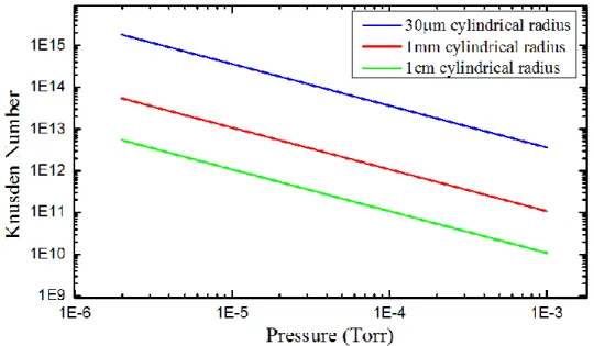
HC-PCF [57]. --- 20 Figure 1-7: Spectral broadening from the transit time (dash line) and atom-wall collisions of core radius
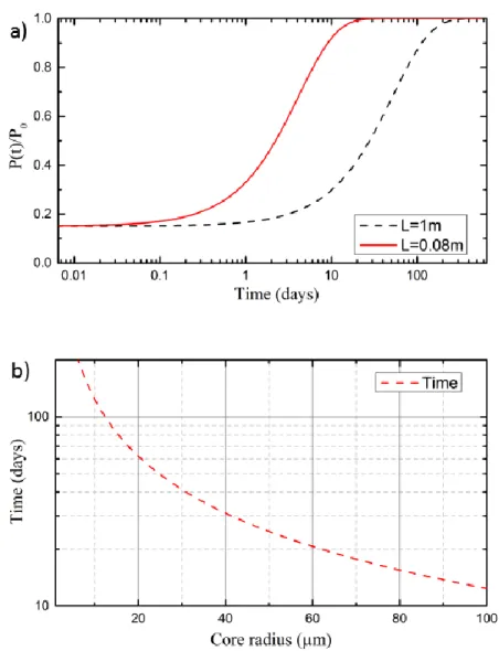
(solid line) dependency. --- 23 Figure 1-8: Knudsen numbers for Rb atom at different pressures with different host cylindrical radius, 30 µm (blue line), 1 mm (red), 1 cm (green). --- 24 Figure 1-9: (a) Molecular (dashed black) loading in 1 m length of HC-PCF with core diameter of 30 µm and
atomic Rb vapour (solid black) loading dynamics in 80 mm length of Kagome HC-PCF with 30 µm diameter hollow core, (b) Characteristic Rb vapour loading time as a function of hollow-core radius. - 27 Figure 2-1: Density of photonic states (DOPS) of a triangular lattice photonic bandgap with a given silica/air fraction [15]. --- 45 Figure 2-2: Principle of PTBM. (a) Dispersion curve of fundamental and second higher-order modes of a
silica rod and (b) Dispersion diagram of an array of silica rods spatially jointed [15, 21]. --- 47 Figure 2-3: (a) SEM image of PBG HC-PCF, (b) SEM image of cladding structure of PBG HC-PCF, (c)
model of unit cell in cladding structure, (d) DOPS for PBG HC-PCF, observed modes by scanning near field optical microscopy (SNOM) (e) silica apex mode, (f) silica strut mode, (g) cladding air hole mode [15,21]. --- 48 Figure 2-4: Effective indices of cladding modes calculated at high normalized frequency for six different cladding structures. Left column: varying apex radius r (top) r = 0.10Λ, (middle) rc = 0.15Λ and
(bottom) r = 0.20Λ with constant strut thickness t = 0.05Λ. Right column: varying strut thickness t (top)
t = 0.005Λ, (middle) t = 0.010Λ and (bottom) t = 0.015Λ with constant apex radius r = 0.15Λ [22]. -- 49
Figure 2-5: (a) Top left: SEM image of a triangular-lattice PBG HC-PCF. Bottom left: near field profile of the fundamental core mode. Right: DOPS diagram of a PBG HC-PCF and for Kagome-lattice HC-PCF. (b) Same representation for the case of IC HC-PCF [13]. --- 50 Figure 2-6: (a) Core guiding mode of Kagome lattice HC-PCF, (b) Fast oscillating cladding mode of Kagome
HC-PCF. Middle image is the intensity plot of (a) core mode (b) cladding modes [22] along length Λ identified by dashed line. --- 51 Figure 2-7: Illustration of the enhanced IC guidance by using hypocycloid core contour. (a) Idealized
M. Ximeng ZHENG | Thèse de doctorat | Université de Limoges | x
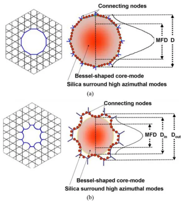
profile distribution of core mode field which diameter is related to core boundary .(b) The same for a hypocycloidal Kagome HC-PCF [24]. --- 53 Figure 2-8: (a) Illustration of hypocycloidal core shape Kagome HC-PCF; (b) Definition of the negative
curvature parameter b [38]. --- 55 Figure 2-9: (a) Numerical simulations of confinement loss spectrum of hypocycloidal curvature dependency.
(b) Fiber model with different curvature b parameters. c) Confinement loss evolution with b for the fundamental band (1000 nm) and the first high order band (500 nm) [38]. --- 55 Figure 2-10: (a) SEM images for different core contours Kagome HC-PCFs, (b) Measured transmission loss
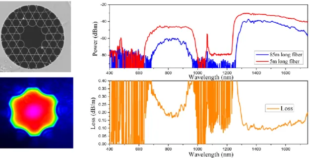
spectrum for different b curvature parameter Kagome HC-PCFs, (c) Experimental and simulated transmission loss at 1500 nm [38]. --- 56 Figure 2-11: SEM image (left top), modal content (left bottom), transmission spectrum and loss spectrum (right) of the fabricated fiber for post-processing. --- 60 Figure 2-12: SEM image (left top), modal content (left bottom), transmission spectrum and loss spectrum
(right) of the four fabricated fiber selected for relaxation measurement. --- 62 Figure 2-13: SEM image (left top), modal content (left bottom), transmission spectrum and loss spectrum
(right) of the fabricated fiber for sub-Doppler transparencies experiment. --- 62 Figure 3-1: Comparison between the IC-PMC and PBG-PMC.--- 71 Figure 3-2: Illustration of the fiber tapering procedure using core vacuum method with the referred sections.73 Figure 3-3: (a) Cross section of un-tapered and (b) tapered IC Kagome HC-PCF fiber at the waist region with an outer diameter respectively of 300 µm and 125 μm. In inset: zoom in of the core-contour showing the preservation of the curvature shape before and after the tapering. (c) Evolution of the down-taper region of fiber with length [40]. --- 74 Figure 3-4: IC fiber tapering images with (a) and (b) without core vacuum resulting in the hypocycloid core shape --- 75 Figure 3-5: Measured transmission spectra of 3 m long HC-PCF with a tapered section from an OD of 300
µm to 200 µm with a full length of 4 cm (TL = 15 mm and waist section length of 10 mm) (blue curve) and of the cut-back at the start of the tapered section (red curve). Full taper loss spectrum (yellow curve). --- 76 Figure 3-6: (a) Evolution of the loss at 1550 nm of several independent whole tapered fibers for three
different DR (300 µm to 200 µm: green line, 300 µm to 150 µm: blue line and 300 µm to 125 µm: red line) and for different TL (5 mm, 10 mm, 15 mm and 20 mm) and (b) for only the down-tapered fiber section. --- 77 Figure 3-7: Evolution of the near field for two tapers differentiated by different TL, referred by 1 (TL = 5
mm and DR = 300/125) and 2 (TL = 20 mm and DR = 300/125) recorded by launching 1550 nm laser source. --- 78 Figure 3-8: Measured splicing transmission spectrum of tapered Kagome-SMF (blue line) the cutback (red
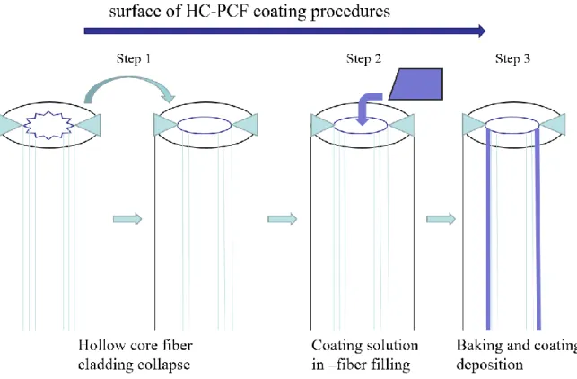
line) and the insertion loss spectrum (black line) for the two sides launching. (a) Light is injected from 300 µm-OD Kagome section by a SMF; (b) Light is injected from SMF to the 125 µm-OD Kagomé section. In inset the images of the splice are shown. --- 79 Figure 3-9: Images of two types of sleeve splicing by using (a) a dual or(b) a single sleeve scheme. --- 82 Figure 3-10: Illustrations of the coating procedures of hollow-core PCF cladding collapse, coating solution
filling and coating deposition. --- 85 Figure 3-11: Images showing the HC-PCF fiber-tips: before (left side) and after (right side) the cladding
M. Ximeng ZHENG | Thèse de doctorat | Université de Limoges | xi
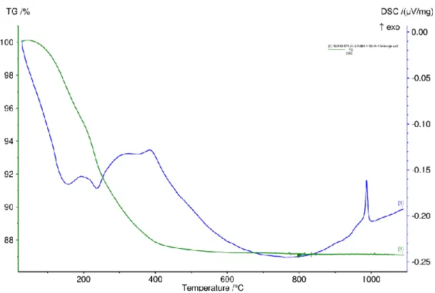
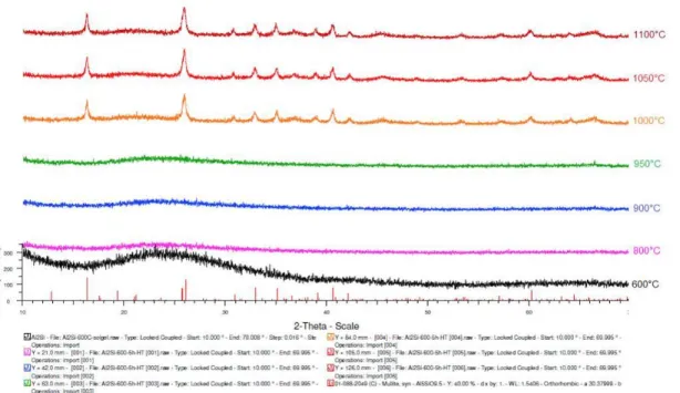
Figure 3-12: Experimental Alumino-silicate sol-gel concentration and crystallization versus the temperatures fitted by Netzsch thermokinetic software. TG: Thermos-gravimetry (green curve), DSC: Differential Scanning Calorimetry (blue curve). --- 87 Figure 3-13: Measured of the sol-gel deposition structure by X-ray diffraction function of the temperatures.88 Figure 3-14: SEM images of sol-gel Kagome HC-PCF inner wall coating treated at different temperatures. 89 Figure 3-15: SEM images of deposition layer thickness obtained inside the HC-PCFs versus the drying
temperature. --- 90 Figure 3-16: SEM images for different pumping velocity and synthesis procedures. --- 91 Figure 3-17: SEM images of coating layers made for different solution concentrations of 0.8 mol.L-1 and 0.1
mol.L-1. --- 91 Figure 3-18: Transmission spectrum measured for PDMS coated and uncoated Kagome HC-PCFs. --- 92 Figure 3-19: Measured Rb D2 absorption lines of Rb vapor contained in Kagome HC-PCFs and vacuum
chamber. In vacuum (blue dash line) for reference, in sol-gel coated Kagome HC-PCF (solid orange) and in uncoated Kagome HC-PCF (dash green). --- 95 Figure 3-20: (a) Evolution of Rb absorption contrast in vacuum (green dots), uncoated capillary (blue dots),
sol-gel coated (red dots) and uncoated Kagome HC-PCF (black dots); (b) Zoom during the last 100 hours. --- 96 Figure 4-1: a) Refractive index n± varies near atomic resonance due to orientation in hyperfine structure of
85Rb at atomic density n = 1012 cm-3, b) optical rotation due to difference in n
± from c) variation of
refractive index n± near atomic resonance due to alignment d) optical rotation due to difference n± [24].111
Figure 4-2: Transition scheme of 85Rb, F=3 D2 absorption line, with optical pumping process and atomic population thermal contribution due to the wall collision. --- 112 Figure 4-3: (a) Experimental set-up for probing atomic polarization state of Rb vapor loaded in HC-PCFs.
ISO: isolator; PD: photodetector; PBS: polarizing beam-splitter, NPBS: non-polarizing beam-splitter. HWP: half waveplate, and QWP: quarter waveplate. (b) System maintaining PDMS, sol-gel coated and uncoated HC-PCFs in the UHV chamber. (c) Chopping decay and probe beam polarization rotation signal. --- 113 Figure 4-4: Remind of the IC Kagome fibers used for ground state atomic polarization investigation. (a) SEM
images of the four fibers differing by core contour, cell defect and radii. (b) Corresponding transmission spectrum in the region of interest. --- 114 Figure 4-5: Measured optical rotation relaxation time for different HC-PCF and classified by core inner wall
surface materials. --- 116 Figure 4-6: Illustration of the dynamic of atomic flying and collision in the HC-PCF. --- 119 Figure 4-7: Numerical simulations for (a) Seven Zeeman sublevels population evolution in the presence of
optical pumping process in fiber #1. (b) Atom polarization lifetime evolution with pump laser intensity of 18 mW/cm2 and detuning of 700 MHz (solid red curve), 800 MHz (dotted orange curve) and 900 MHz (dashed green curve). (c) Population build-up time versus the pump frequency detuning with the intensity of 18 mW/cm2 (solid red curve), 36 mW/cm2 (dashed orange curve), 54 mW/cm2 (dashed green curve), 72 mW/cm2 (dashed blue curve). (d) The effective transverse speed probability density function for the polarized atoms (red curve). For comparison the Rb thermal Maxwell-Boltzmann distribution is shown (blue filled curve) (from reference [20]). --- 120 Figure 4-8: Monte-Carlo simulation calculated (green triangles) and measured (orange stars) τ1. For atom-wall relaxation time for the tested four fibers. The theoretical thermal atom transit time τtt (red) and
dwell time τdw (blue) are also indicated. --- 122
M. Ximeng ZHENG | Thèse de doctorat | Université de Limoges | xii
Figure 4-9: Experimental systematic study of polarization rotation relaxation time based on different Kagome fiber inner core sizes and curvature b parameters. The dashed curve represents the simulation results.123 Figure 4-10: Relaxation time pump beam power dependency in different coated Kagome fibers. The dwell time for each surface materials are backstairs obtained when the pump beam is saturated. --- 125 Figure 4-11: Experimental setup for measuring the atomic polarization relaxation by using different input
lasers. ISO: isolator; PD: photodetector; PBS: polarizing splitter, NPBS: non-polarizing beam-splitter. HWP: half waveplate, and QWP: quarter wavelplate.--- 127 Figure 4-12: Polarization rotation relaxation time of detuning frequency dependency of probe beam with fixed pump blue detuning 800 MHz off resonance to the 85Rb, F=3. The probe beam detuning in the range of 7 GHz which cover all four absorption lines. --- 127 Figure 5-1: The adatoms fraction for the case of room temperature of 293 K (red and blue curves) and T =
370 K (dark blue and green curves) and for 𝜏0 = 1 𝑝𝑠 (red and dark blue curves) and 𝜏0 = 1 𝑛𝑠 (blue and green curves). The symbols correspond to 𝑛𝑎𝑑𝑛 deduced from 𝜏0 and 𝐸𝑎 found references [3], [19] and [20]. --- 137 Figure 5-2: Surface-atom potential for the case of Rb ground state and for different ranges of the atom-surface distance. The black curve corresponds to 6-12 type potential (equation 5-1) with the parameters taken from reference [11]. The red curve corresponds to the potential of equation 5-3 with the parameters taken from reference [14]. --- 140 Figure 5-3: Surface-atom potential profile as experienced by a Rb atomic inside and a 60 m diameter core
of HC-PCF for the D2 transition ground (red curve) and excited state (blue curve). --- 143 Figure 5-4: The sub-Doppler features are generated by a circular polarization laser beam in Rb-filled
capillary. The magnetic field is 5.5 G and the beam power is ~ 2000 μW with beam waist of 1.5 mm. The Doppler feature is at 85Rb, F=3 D2 absorption line. (From[5]) --- 145 Figure 5-5: Experimental setup for sing laser beam generated sub-Doppler transparencies. ISO: isolator,
ECDL: external cavity diode laser, QWP: quarter waveplate, PBS: polarization beam splitter. --- 147 Figure 5-6: Typical spectra. Absorption spectrum from a macroscopic cell (reference cell) (a). The fiber
transmitted spectrum of the polarized power 𝑃 ∥ along one of the PBS axis (b), of the polarized power 𝑃 ⊥ along the second PBS axis (c), of total power 𝑃 ∥ +𝑃 ⊥ ((c), and of the difference 𝑃 ∥ −𝑃 ⊥. The spectra were obtained from the same HC-PCF but with different core inner-surface. The red curves correspond to an uncoated silica inner-surface, the green curves to sol-gel ceramic coated surface and the blue curves to the PDMS coated surface. The spectra were recorded with 0 G DC magnetic field, 150 μW laser power. The laser is circularly polarized, and the temperature was 100 Celsius. --- 148 Figure 5-7: (a) P// spectral evolution of 85Rb-filled HC-PCF D2 absorption lines (left column), and a zoom in
at the SDL of the F=3F’ Doppler line. Here, the DC magnetic field is 45 G, beam power ~ 150 μW, temperature: 100 ˚C. --- 150 Figure 5-7: (b) P spectral evolution of 85 Rb-filled HC-PCF D2 absorption lines (left column), and a zoom in at the SDL of the F=3F’ Doppler line. Here, the DC magnetic field is 45 G, beam power ~ 150 μW, temperature: 100 ˚C. --- 151 Figure 5-8: Frequency shifts and variations of amplitude of sub-Doppler feature on 85Rb, F=3 line, as the
waveplate angle is varying. (a) & (b) for the polarization component P⊥ and (c) & (d) for the polarization component P//. --- 152 Figure 5-9: (a) Polarization component P// spectral evolution of 85Rb-filled HC-PCF D2 absorption lines (left
column), and a zoom in at the SDL of the F=3 F’ Doppler line. Here, the DC magnetic field is 45 G, beam power is varied from 50 μW to 300 μW, temperature: 100 ˚C. --- 153
M. Ximeng ZHENG | Thèse de doctorat | Université de Limoges | xiii
Figure 5-9: (b) Polarization component P spectral evolution of 85Rb-filled HC-PCF D2 absorption lines (left column), and a zoom in at the SDL of the F=3 F’ Doppler line. Here, the DC magnetic field is 45 G, beam power is varied from 50 μW to 300 μW, temperature: 100 ˚C. --- 154 Figure 5-10: Show the frequency shifts and the enhancement of amplitudes of SDL on 85Rb, F=3 line, as the
operational power increasing. (a) & (b) for the polarization component P⊥ and (c) & (d) for component P//. --- 155 Figure 5-11: (a) Polarization component P// spectral evolution of 85Rb-filled HC-PCF D2 absorption lines (left
column), and a zoom in at the SDL of the F=3 F’ Doppler line as the magnetic field increasing. Here, the magnetic field varies from 0 Gauss to 45 Gauss, laser beam is circular polarization with 150 μW operational power, temperature: 100 ˚C. --- 156 Figure 5-11: (b) Polarization component P spectral evolution of 85Rb-filled HC-PCF D2 absorption lines
(left column), and a zoom in at the SDL of the F=3 F’ Doppler line as the magnetic field increasing. Here, the magnetic field varies from 0 Gauss to 45 Gauss, laser beam is circular polarization with 150 μW operational power, temperature: 100 ˚C. --- 158 Figure 5-12: Show the frequency shifts and the enhancement of amplitudes of SDL on 85Rb, F=3 line, as the
magnetic field increasing. (a) & (b) for the polarization component P⊥ and (c) & (d) for component P//.159 Figure 5-13: Magnetic field dependence of SDL with different magnetic field directions. Spectra in left
column are the variations of absorption lines with positive magnetic field, b) with negative magnetic field. And the residential SDLs in the Doppler lines 87Rb, F=2 c) & d), 85Rb, F=3 e) & f), 85Rb, F=2 g) & h). All spectra are the polarization component P// evolution. --- 161 Figure 5-14: Show the evolutions of SDL on different surface materials (a), and with different temperatures (b). --- 163 Figure 5-15: (a) Schematic representation of the energy level of VdW potential for Rb atoms at the surface
for the D2 line transition, showing the atom-wall interaction mediated energy exchange between the different vibrational levels of the atom in the ground state and the excited state of 85Rb D2 transitions. (b) Calculated VdW potential vibrational states energy levels and ranges for orders n between 275 and 280. --- 165 Figure 5-16: The laser frequency dependence of normalized pumping rate |5S1/2 F = 3,νs⟩→|5P3/2 F’=2,3,νp⟩
→|5S1/2 F = 3,νs’⟩ for several values of parameter r0. Left: r0=0.2 nm, center: r0=0.6 nm, right: r0=1.4 nm. --- 166
M. Ximeng ZHENG | Thèse de doctorat | Université de Limoges | xv
List of tables
Table 1-1: Comparison of atom-confined photonic structures ……….. 19 Table 2-1: Developed state-of-the-art fibers for atomic applications ……… 57 Table 2-2 Physical integrities of experimental fiber samples in this thesis ………... 59 Table 3-1: Silicate and Borosilicate glass properties ………. 81 Table 3-2: Single and dual sleeve splicing loss ……….. ……... 82 Table 3-3: Properties of different anti-relaxation coating for comparison ………. 94 Table 4-1: Atomic density, physical properties of different Rb loaded in Kagome HC-PCFs ……… 116 Table 4-2: Measured τφ and associated τ1 for the different Kagome HC-PCF under test ………... 116 Table 5-1: Values of Ea and τ0 reported in the literature for different atoms and surfaces …………. 137
M. Ximeng ZHENG | Thèse de doctorat | Université de Limoges | xvii
Abbreviations
ARROW Anti-resonant reflecting optical waveguide
CMOS Complementary metal-oxide-semiconductor
CPT Coherent population trapping
CQED Cavity quantum electrodynamics
CSAC Chip Scale Atomic Clock
CSAM Chip scale atomic magnetometer
CW Continuous wave
DOPS Density of photonic state
DR Down-ratio
DSC Differential scanning calorimetery
ECDL External cavity diode laser
EIT Electromagnetically induced transparency
FEM Finite element method
FM Fundamental mode
FOM Figure of merit
FOR Fire of ring
FWHM Full width at half maximum
HC-PCF Hollow-core photonic crystal fiber
HHG High harmonic generation
HOM Higher order mode
HWP Half wave plate
IC Inhibited coupling
ID Inner diamter
IR Infrared
ISO Isolator
LIAD Light induced atomic desorption
LID Light induced drift
LJ Lennard-Jones
MAC Miniature atomic clock
MEMS Micro-electronic mechanical systems
MFD Mode field diameter
MFP Mean free path
M. Ximeng ZHENG | Thèse de doctorat | Université de Limoges | xviii
NEP Noise equivalent power
NF Near field
NIR Near-Infrared
NPBS Non-polarizing beam splitter
OD Optical density
ODMS Octadecyldimethylmethoxysilane
OSA Optical spectrum analyzer
OSCC Optical space Cs clock
OTS Octdecyltrichlorosilane
PBG Photonic bandgap
PBS Polarizing beam splitter
PD Photodetector
PDMS Polydimethylsiloxane
PMC Photonic Microcell
PML Perfectly matched layer
PTBM Photonic tight binding model
QWP Quarter waveplate
Rb Rubidium
SAS Saturated absorption spectroscopy
SDL Sub-Doppler lines
SEM Scanning electron microscope
SMF Single mode fiber
SNOM Near field optical microscopy
SNR Signal to noise ratio
SRS Stimulated raman scattering
TBM Tight binding model
TEOS Tetraethoxysilane
TG Thermos-gravimetry
TIR Total internal reflection
TL Transition length
UHV Ultra-high vacuum
UV Ultra-violet
VdW Van der Waals
M. Ximeng ZHENG | Thèse de doctorat | Université de Limoges | 1
Chapter 1
Atom optics in gas confined hollow-core
photonic microstructures
This chapter introduces the physics background of atom optics confined in dielectric micro-structures such as hollow-core photonic crystal fibers and the different efforts being recently undertaken world-wide along with their underpinning motivations. We list the different atom confining geometries that have been explored with a discussion on their respective advantages and disadvantages. Finally, we finish with describing the layout of the thesis chapters.
M. Ximeng ZHENG | Thèse de doctorat | Université de Limoges | 2
1.1 Introduction
Atomic or molecular transitions are widely applied in laser frequency metrology and spectroscopy as a frequency reference for its very weak sensitivity to environmental changes such as pressure or mechanical vibrations [1]. This feature is also explored in other fields such as quantum optics, quantum sensors or quantum information. For example, optical magnetometers in which a magnetic field is probed by observing changes in the properties of light-matter interaction can achieve extremely high sensitivity [2]. Rydberg transitions based on single photon interactions are currently explored for quantum information and computing applications to develop functionalities such as controlled-NOT quantum gate based on Rydberg blockade interactions [3]. Moreover, quantum memory [4], slow light [5], cavity quantum electrodynamics (CQED) [6] are other demonstrations illustrating the impact of atom-laser interaction.
In addition to the above, when laser cooling techniques [7][8][9] are deployed to cool the atoms, one can achieve an extremely high frequency stability level, which is now illustrated in microwave and optical atomic clocks with frequency instability reaching 1 part in 1014 and 1 part in 1017 respectively [10][11][12]. Furthermore, ultra-low temperature cold atoms (i.e. Bose-Einstein Condensates) represent a novel matter phase [13] that led to the emergence of the field of matter wave, and which is used to develop next generation gravimeters [14], gyroscopes [15] based on atomic interference techniques [14].
In parallel to the impressive progress made in the physics and technology of atom optics mentioned above, another pursuit emerged in the last decade which consists in miniaturizing the atom optical systems. Indeed, so far all the best performances of atomic clocks and quantum sensors were achieved in laboratory environment using highly complex set-ups and requiring highly qualified scientists. The motivations of miniaturizing atom optic devices such as atomic clocks or magnetometers are justified by the huge impact such these outstanding laboratory performances would have in both a technological and scientific stand point if delivered in stable and compact devices. An illustration of the impact of the availability of such devices to industry and the world outside specialised
M. Ximeng ZHENG | Thèse de doctorat | Université de Limoges | 3
laboratories is given by the Chip-Scale-Atomic-Clock (CSAC), developed in NIST in the last decade [16], and which is now industrialized in several applications such telecommunications and sub-marine geophysical explorations.
The miniaturization of atom optics systems entails first a drastic size-reduction of the host structure containing atomic and molecular gases. In addition to the technological challenges that this aim implies, reducing the dimensions of the gas host structure could reduce the signal to noise ratio (SNR) of any probed transition if the interaction length with the medium is not appropriately addressed. Secondly smaller gas host systems result in increased level of interactions with the walls of the container, and subsequently in undesired spectral broadening and shifting of atomic and molecular transitions spectral lines. Thirdly, the vicinity of atoms to the host wall surface poses problems in the atoms’ lifetime in such microstructures via the physio-chemical reaction between the atoms and surface. In this chapter we list the different routes explored to develop miniature atom cells and how the above-mentioned challenges are addressed.
Below, we start with a brief overview of the basic physics underlining the key principles of atom-laser interactions and highlighting their relevance to the work presented later. In the following sections of the chapter a review of the work to date on reducing the physical dimensions of the gas host container will be presented. Different methods have been used for reducing the physical dimensions of the gas host, varying from micro-electronic-mechanical systems (MEMS) technology to dielectric waveguide technologies. The use of dielectric waveguiding geometries such as hollow-core photonic crystal fibers (HC-PCF) for hosting gas phase atomic and/or molecular media offers several benefits. It particularly includes a very long interaction length which is possible due to low loss propagation in such waveguide, tight transverse mode confinement and easy integration with existing fiber optic systems. These features mitigate some of the problems involved with reducing the transverse dimensions of the gas host container such as increased atom wall collisions. Miniaturisation of the gas host has become a pressing need to deliver the outstanding performance of atomic vapours to industry and the world outside the laboratory.
M. Ximeng ZHENG | Thèse de doctorat | Université de Limoges | 4
1.2 Basics of atom-light interaction
If we have to single out one key performance indicator to define the performance of an atom-optic device such a frequency reference and subsequently atomic clocks or magnetometers, it would be the magnitude ratio between the quality factor of the transition spectral and the SNR; 𝑄 𝑆𝑁𝑅⁄ . Indeed, the larger this ratio is the more stable the frequency reference is. This means that the linewidth of the transition spectral line must be as small as possible.
Whilst atomic and molecular transitions have an intrinsic fundamental linewidth set by the Heisenberg uncertainty principle, their lines are typically Doppler broadened to hundreds of megahertz by the Maxwell-Boltzmann velocity distribution of the atoms or molecules. This is why several experimental techniques for generating sub-Doppler transparency features in atomic and molecular have been developed and atom/molecule based frequency references. Examples of these techniques are saturated absorption spectroscopy (SAS) [17], electromagnetically induced transparency (EIT) [18][19], coherent population trapping (CPT) [20] and Ramsey interference [21][22]. Such methods are commonly used to generate extremely narrow sub Doppler transparency features for laser frequency stabilisation, atomic clocks and quantum sensors. The generation of such sub-Doppler spectral lines result from either velocity selective transition saturation or setting the atom in a coherent superposition state. Below, after listing the different mechanisms of line spectral broadening, we review the basic physics behind the generation of these sub-Doppler spectral lines.
Spectral line shapes
Atom absorbs photons appear optical absorption and optical lines shape are required resonant or near-resonant to the atomic transition. The experimentally observed linewidth of optical absorption is typically combined and broadened by four main mechanisms named Natural Broadening, Doppler Broadening, Power Broadening and Pressure Broadening. Atomic and molecular transitions are often formed as a Lorentzian oscillator.
M. Ximeng ZHENG | Thèse de doctorat | Université de Limoges | 5
The essential characteristics of the features of the atomic transition includes the quality factor (Q-factor) and signal-to-noise ratio (SNR) accompany with spectral broadening mechanisms which relate to atom or gas medium. These mechanisms limit the minimum linewidth of a spectral feature due to the Doppler broadening. The Lorentzian oscillators can be characterized by using the resonance Q-factor, which is expressed as the ratio of the average energy stored in the resonance and the dissipation rate of the energy.
𝑄 = 𝜔0
∆𝜔, (1-1)
here ω0 is the frequency of the atomic transition and Δω is the linewidth of the
transition. Another characteristic employed in frequency standards and laser metrology is signal-noise-ratio which is combined with Q-factor as the fractional frequency deviations [23][24] and are described as following:
∆𝑓 𝑓 ∝
1
𝑆𝑁𝑅∗𝑄, (1-2)
To minimize the fractional frequency deviation, a high Q-factor or high SNR are preferred. A high SNR can be required by optimizing the atom-light interaction (discussed in section 1.5). Extremely high Q factors have been achieved by laser cooling and trapping [8] (Q ~ 9.8 × 10⁹) and by using metastable optical transitions [10] (Q ~ 1.6 × 10¹³). Generally, a high Q-factor is obtained by minimizing the linewidth of the resonance. The following section will describes the main broadening mechanisms in the spectral features.
The absorption line shape is typically broadened by several processes, including Doppler, collisional, power and transit time. These mechanisms can be broken down into two categories, homogeneous [25, 26], acting on all the atoms in the same manner and inhomogeneous [25–27], a perturbation that depends on the energy state of each atom (e.g. atom velocity). Power and collisional broadening are examples of homogeneous broadening while transit time and Doppler broadening are examples of inhomogeneous broadening because of the dependence on the individual atomic velocities.
M. Ximeng ZHENG | Thèse de doctorat | Université de Limoges | 6 A. Natural Broadening
Natural broadening is the reason of quantum uncertainty in spontaneous emission of energy level. The interval energy level ΔE, in the form of the Heisenberg uncertainty principle is
Et ћ. (1-3) The uncertainty in time is the natural lifetime, ∆t = τnat. The uncertainty in frequency
is ∆ν = ∆E/2πћ, giving the natural linewidth Γnat = ∆ν = 1/2πτnat. The excited states for
example for Rb atom, 2P1/2 and 2P3/2 states, have natural lifetime τnat around 25 -35 ns. For
the D1 and D2 transitions of alkali atoms, the natural linewidth is about 4-6 MHz. This magnitude of broadening mechanism is much smaller than other contributions which presents Lorentzian distribution. Ultimately the linewidth of an atomic transition can be reduced to this quantum limit.
B. Doppler Broadening
Doppler Broadening of atomic resonance lines is caused by the Doppler Effect, which the motional atom or molecular defined by temperature cause the absorbed light frequency shift from the resonance frequency as:
ν = ν0(1 − 𝜐𝑧
𝑐), (1-4)
Thus, the atomic population absorbs the off-resonance light. The probability P(υz)dυz
of an atom having a velocity in the range from υz to υz +dυz is given by the Maxwellian
distribution 𝑃(𝑣𝑧)𝑑𝑣𝑧 = ( 𝑚 2𝜋𝑘𝐵𝑇) 1 2𝑒−𝑚𝑣𝑧2/2𝑘𝐵𝑇𝑑𝑣 𝑧, (1-5)
resulting in the full width at half maximum (FWHM),
𝛤𝐺 = 2𝑣0
𝑐 √ 2𝑘𝐵𝑇
M. Ximeng ZHENG | Thèse de doctorat | Université de Limoges | 7
Doppler broadened linewidth of the D1 transition for 85Rb and 87Rb atom at room temperature is about 480 MHz [28]. The FWHM temperature dependency can be decreased by limiting the atom motion such as laser cooling [29][30].
C. Power Broadening
The power broadening is the dependence of the light intensity appeared on the spectral linewidth broadening. Typically, power broadening is observed as a Lorentzian profile when continuously monitored. For example, the excited state population in a two level system are interacted with a CW laser. The increase of laser intensity for any detuning causes more population to go to the excited state, so the signal is enhanced. The transition linewidth is the range of detuning for which the excited state acquires considerable transient population during the transit process. The range is broadened when the laser intensity increases, therefore power broadening is observed. As the host of quantum sensor, the operated light intensity in HC-PCF should be as low as possible to limit the power broadening and the stack shift from light [31].
D. Collisional Broadening
Atom-atom collisions and atom-wall collisions perturb the atoms with reduced lifetime in the excited state. This pressure dependent mechanism results in both a shift and broadening of the optical absorption line. The magnitudes of these phenomena are proportional to the number of perturbing atoms or gas molecules which are referred to the pressure shift and pressure broadening. This contribution of spectral broadening is a homogeneous effect therefore a Lorentzian distribution. Otherwise, the magnitude of collisional shift is much lower than the collisional broadening. The atom-wall collision in HC-PCF is enhanced due to the micro-meter geometric core size.
M. Ximeng ZHENG | Thèse de doctorat | Université de Limoges | 8
Coherence
According to quantum mechanics principles, the state of a quantum system such as an atom can be either in one of its eigenstates or in a superposition of these eigenstates. In this case, the latter exhibits a phase relationship between them and the resulting state is coined a coherent state. In practice, the coherent state is generated by one or more laser field resonant with atomic transition states. The stimulated electric dipole oscillations are strongly enhanced when the laser frequency is detuning close to the resonant frequency which is the phase relation between the field-induced coupled-states. The simplest coherence effect can be observed in a 2-level system driven by a laser frequency ω. The population of the ground state in such a system can be depleted to minimize spontaneous emission. Therefore, stimulated absorption and stimulated emission processes repeatedly oscillates between the ground state and the excited state. This process is known as Rabi oscillations and the coupling between the two states occurs at the oscillation frequency, called the Rabi frequency and given by
𝛺𝑅 = √𝛺02+ ∆2
2
, (1-7) where Δ is the detuning frequency from the resonance and
𝛺0 = 𝜇∙𝛦0
ћ . (1-8)
E0 is the amplitude of the electric field, μ is the transition electric dipole moment and
ћ is reduced Planck constant. The Rabi frequency is generally used to take into account both the transition strength and the laser intensity thereby characterizing the light-matter interaction.
Figure 1-1 (b) shows the Rabi oscillations in two level system for different detuning frequency from resonance, Δ = 0, Ω0, 2Ω0 (color curves respectively). In fact, the
population in higher energy level has natural limited life time and decays at a rate given by spontaneous emission γsp. Such decay rate is strongly enhanced by external physical
M. Ximeng ZHENG | Thèse de doctorat | Université de Limoges | 9
The dephasing mechanisms could originate from any of the line broadening effects mentioned above. These dephasing strongly attenuate such an oscillation (coherence). If we limit these mechanism to those of collisional origin, then the coherence decay takes the following form given by 𝛾𝑠𝑝
2 + 𝛾𝑐𝑜𝑙𝑙. Here, γcoll is the collision induced coherence decay.
Figure 1-1 (c) shows Rabi oscillations with different dephasing rates (γo-black curve and
5γo-blue curve) resulting in damping of the oscillation as the relative phase relation
between the levels is disrupted. Given that often the dephasing rate is always greater than the spontaneous emission limit, engineering coherence is extremely challenging and any resulting coherence is fragile and sensitive to perturbations.
Figure 1-1: (a) 2-level atomic system resonant with frequency ω0 interacted by laser field frequency
ω. (b) Rabi oscillations of a 2-level atomic system with different detuning frequencies, Δ=0 (black line), Δ=Ω0 (blue line), Δ=2Ω0 (red line). c) Rabi oscillations of a 2-level atomic system including
M. Ximeng ZHENG | Thèse de doctorat | Université de Limoges | 10
Sub-Doppler transparencies generated techniques
A. Saturated Absorption Spectroscopy (SAS)
One of generating sub-Doppler features technique is saturated absorption spectroscopy (SAS), which does not depend on the coherence effect between atomic states but rely on the thermal atom velocity selection through optical pump process. The experimental configuration consists on using counter-propagate scheme through the atom medium which includes a single laser beam derived into one higher pump beam and one weak probe beam. This is described by using the population rate equations and can be realized by using only one single laser source. In the case of one single laser source, an individual atom at a velocity v cannot be resonant with the two fields (the same frequency) at the same time for a given transition. Once the atom is on resonance with pump beam, the atomic population of the ground state are fully pumped to the excited state and become saturated so that the counter-propagating weak probe beam will not interact with this atomic transition and appear transparent on the absorption lines. The sub-Doppler transparencies are recorded with the Doppler broadened absorption lines due to the Doppler effect of the thermal atom across the resonant transition. SAS was firstly and experimentally demonstrated in acetylene medium by Labachelerie et al. [32], by using a high finesse Fabry-Perot cavity in order to provide a sufficient interaction length for the laser-matter interaction. A linewidth of ~ 2 MHz is reported in this reference which feature linewidth can be as narrow as the power broadened linewidth and SAS have been extensively used in laser stabilization schemes.
B. Coherent Population Trapping
Coherent population trapping (CPT) was first demonstrated by Alzetta et al. in 1976 [33], and this was very shortly reviewed by Arimondo et al. [34] which is considered as coherent effect in a Lambda type 3-level systems. It was understood that the atoms were optical pumped into a dark state by two excitation beams. When the detuning between these two excitation beams is equal to the detuning of the two states, it will form a
non-M. Ximeng ZHENG | Thèse de doctorat | Université de Limoges | 11
dipole allowed transition whereby the state cannot spontaneously decay hence the atoms are trapped.
Figure 1-2: Schematic of three level system with related parameters: Δ1 and Δ2 are the detuning
frequency from the resonance of each laser field which Δ1=ω31-ω1 and Δ2=ω32-ω2 respectively. Γ31 and
Γ32 are the decay terms from the excited state to the two ground states.
The dark state was created by the interferences between two excitation levels from two ground states to a common excited state. This required Λ-type 3-levels system shown in fig. 1-2. Customarily, the laser resonating with the |1> ↔ |2> transition is called the probe laser, and the beam driving the |2> ↔ |3> transition is called the control laser. Both transitions are electric-dipole allowed transitions. Δ1 and Δ2 are the detuning frequency from the
resonance of each laser field which Δ1=ω31-ω1 and Δ2=ω32-ω2 respectively. Γ31 and Γ32 are
the spontaneous decay rates from the excited state to the two ground states, are about 1- 10 MHz.
In the experimental conditions, the presence of the laser fields changes the eigenstates of the Hamiltonian of atom-laser system thus the atom eigenstates are linear overlapped:
|𝛼+⟩ = sin 𝜃 sin 𝛷 |2⟩ + cos 𝛷 |3⟩ + cos 𝜃 sin 𝛷 |1⟩
|𝛼0⟩ = sin 𝜃|1⟩ + cos 𝜃 |2⟩, (1-9)
|𝛼−⟩ = sin 𝜃 cos 𝛷 |2⟩ + sin 𝛷 |3⟩ + cos 𝜃 cos 𝛷 |1⟩
M. Ximeng ZHENG | Thèse de doctorat | Université de Limoges | 12 tan 𝜃 =𝛺𝑝 𝛺𝑐, (1-10) and tan 2𝜃 = √𝛺𝑝2+𝛺𝑐2 𝛥 , (1-11)
The detuning of the probe laser formed as the dressed states and the second formula in Eq. 1-11 indicates the formation of dark state |α0> when no decoupling from |3> state, any
population spontaneous decay to the |α0> state becomes population trapped here. Thus two
lasers are required to be phase coherent hence the dark overlap state can be formed.
C. Electromagnetically Induced Transparency (EIT)
Electromagnetically induced transparency (EIT) is a coherent effect but works on a slightly different principle compare to CPT, which phenomenon usually appears in the regime where the control laser is much stronger than the probe laser, i.e. Ωp ≪ Ωc, and
only the population of the state |1> has considered to be pumped completely. EIT phenomenon was first experimental observed by Harris et al. in strontium vapor cell [36]. Under the condition of Ωp ≪ Ωc, the strong control laser shifts the energy levels away from
the resonant center via AC stack effect, which can be understood as the creation of dressed states in atom-light system [37]. When the stack shift is equal to the Rabi frequency of the control laser, the absorption of the probe laser splits into a classic Autler-Townes doublet which splitting frequency is equivalent to the control laser Rabi frequency, and results an enhanced transparency at the resonant center-electromagnetically induced transparency.
M. Ximeng ZHENG | Thèse de doctorat | Université de Limoges | 13
Figure 1-3: (a) Dressed states in atom-light system (b) Λ-type of 3-level system includes two coherent pathways |1>-|3> (black line) and |1>-|3>-|2>-|3> (red line).
In the case of Ωp ≪ Ωc, the three dressed states can be simplified to give in the
following equations: |𝛼+⟩ = 1 √2(|2⟩ + |3⟩) |𝛼0⟩ =|1⟩, (1-12) |𝛼−⟩ = 1 √2(|2⟩ − |3⟩)
The schematic of dressed states is shown in fig. 1-3 (a). When a probe laser is applied to scanning across the bare states |2> and |3>, a modified absorption profile for these two dressed states is recorded. And the ground state is unmodified in the second equation. Considering interference pathways in a Λ-type 3-level system, the coupling laser which couples the states |2> and |3> through the available pathways to the excited state (|1>- |3> or |1>- |3>- |2>- |3>) has much higher Rabi frequency than the probe laser. Therefore the transit probability for these two pathways are quite similar and coherent, which lead to the absorption cancellation [38].
M. Ximeng ZHENG | Thèse de doctorat | Université de Limoges | 14
Figure 1-4: 3-level atom-light interaction system. a) Lambda (Λ) system, b) Vee (V) system, c) ladder system.
In EIT, there also exists quantum interference but mainly when the control laser Rabi frequency is in the order of the excited state linewidth. The destructive interference between the transit pathways of ground state to the induced dressed states is important in Λ-type systems [39], shown in fig. 1-4 (a). The interference results in the probe absorption being zero at the resonant center. Furthermore, the dressed state interference is not the main role in V-type (fig. 1-4 (b)) and ladder systems (fig.1-4 (c)) [40].
1.3 Compact host for atomic optics
The effort in miniaturizing atom or molecular cells for atom-optic related devices started in the 2000s. Two main classes of integrated or compact technologies have since been developed by several research groups. These are summarized in fig. 1-5. The first class to confine the atoms is a solution based on Micro-electronic-mechanical systems (MEMS) technology, and where by the atoms cell is sandwiched in layered architecture between integrated laser source and photodetector. The second class is based on dielectric waveguides where the gas cell acts as a harboring platform for the atoms and a light guidance. The first of these components is hollow-core photonic crystal fibers (HC-PCF), which has been transformed into a photonic microcell (PMC) by filling the fiber core with a given gas [41][42]. The most elaborate form of PMC consists of a gas filled HC-PCF that
M. Ximeng ZHENG | Thèse de doctorat | Université de Limoges | 15
is hermetically sealed by splicing its both ends to solid fibers. However, so far this all-fiber PMC has been limited to molecular gases, and atom vapor PMC is still to be developed. In parallel to HC-PCF, CMOS compatible resonant reflecting optical waveguides (ARROW’s) have also been developed as atom cells [43][44].
Below a briefly overview on these atom-optic components. It is noteworthy that other schemes have or are being pursued, such as tapered nano-fiber, however, we limit our survey to those which acts as atom cells.
Compact quantum sensors in electronic structure: Chip Scale
Atomic Clock (CSAC) and Chip Scale Atomic Magnetometer
(CSAM)
The Chip Scale Atomic Clock (CSAC) program was initiated by DARPA in 2002. And very soon later, a micro fabricated atomic clock was reported by Knappe et al. in 2004 [16]. A MEMS-based atomic clock [16] and atomic magnetometer [45] was then reported by S. Knappe et al. in 2004 and become commercial device available now. This
Figure 1-5: Illustrations of two compact solutions for atom and gas confined host. Left images are exciting electronics structure based on MEMS technology, right images are developing
M. Ximeng ZHENG | Thèse de doctorat | Université de Limoges | 16
miniaturization units are low cost repeatable manufactured and stable. For such a MEMS-based atomic clock, a volume of 10 mm3 of this device could have a fractional frequency stability of 2.5×10⁻¹⁰ s-1, and is featured with 7.1 kHz linewidth of Cesium atom sub-Doppler feature.
This device fulfils many of the requirements for a compact frequency standard such as reasonable short term stability, compact size and low power consumption. However the device requires external temperature and current control which adds to the size. Also the interaction length with the Cs vapour is extremely short because of the compact size as such the contrast of the frequency reference is extremely small, 0.91% of the total absorption line strength. For compact magnetometer, a chip-scale atomic magnetometer [46] has been implemented at NIST which is based on the D1 absorption line of 87Rb atoms. The active interaction volume of this magnetometer is 1 mm3 and can measure the magnetic fields with a sensitivity of 50 pT Hz-1/2 over a frequency range of 10-100 Hz. It is the first chip-scale magnetometer based on an MEMS atomic vapor cell with comparable sensitivity to cost magneto-resistive sensors. New generation of Miniature Atomic Clock (MAC) SA.35m was released in 2012 by Microsemi et al. and could have a frequency accuracy of 3*10-11 per second with Rubidium, operation beam power is 12 mW and the weight is less than 100 g. In Parallel, some European projects such as MUSO project and CSEM project in Swiss, Optical space Cs clock (OSCC) project in France for Galileo system, have been established to develop miniature atomic clocks.
Finally, while the design is fully integrated it relies upon traditional free space propagation scaled down to the device size opposed to the following devices which are all waveguiding based designs, hence do not suffer from misalignment of optics.