HAL Id: tel-03222173
https://tel.archives-ouvertes.fr/tel-03222173
Submitted on 10 May 2021
HAL is a multi-disciplinary open access archive for the deposit and dissemination of sci-entific research documents, whether they are pub-lished or not. The documents may come from teaching and research institutions in France or abroad, or from public or private research centers.
L’archive ouverte pluridisciplinaire HAL, est destinée au dépôt et à la diffusion de documents scientifiques de niveau recherche, publiés ou non, émanant des établissements d’enseignement et de recherche français ou étrangers, des laboratoires publics ou privés.
to functionalized interposer
Julio Mota Pinheiro
To cite this version:
Julio Mota Pinheiro. Development of passive circuits in nanowire-membrane technology in mil-limeter wave frequencies : application to functionalized interposer. Micro and nanotechnolo-gies/Microelectronics. Université Grenoble Alpes [2020-..]; Universidade de São Paulo (Brésil), 2020. English. �NNT : 2020GRALT024�. �tel-03222173�
Pour obtenir le grade de
DOCTEUR DE L’UNIVERSITE GRENOBLE ALPES
préparée dans le cadre d’une cotutelle entre la
Communauté Université Grenoble Alpes et
l’Université de São Paulo
Spécialité : Nano Electronique et Nano Technologies
Arrêté ministériel : le 6 janvier 2005 – 25 mai 2016 Présentée par
Júlio MOTA PINHEIRO
Thèse dirigée par Philippe FERRARI et par Ariana SERRANO et codirigée par Gustavo REHDER
préparée au sein des Laboratoires RFIC-Lab et Laboratoire de Microélectronique de l’USP
dans le École Doctorale EEATS et le PPGEE de l’EPUSP
Development of passive circuits
in nanowire-membrane
technology in millimeter wave
frequencies: application to
functionalized interposers
Thèse soutenue publiquement le 24/07/2020 devant le jury composé de :
Mme. Fatima CORRERA
Professeur à l’Université de São Paulo, Président M. Tinus STANDER
Professeur à l’Université de Pretoria, Rapporteur M. Hervé AUBERT
Professeur à l’Institut National Polytechnique de Toulouse, Rapporteur M. Jean-Marc DUCHAMP
Maître de conférences à l’Université Grenoble Alpes, Membre Mme. Ariana SERRANO
Professeur à l’Université de São Paulo, Membre M. Philippe FERRARI
milimétricas no interposer denominado MnM – metallic nanowire-filled membrane. Esse interposer está inserido no contexto onde a miniaturização dos circuitos passivos devido a elevada frequência de operação (grosso modo acima de 10 GHz até 300 GHz para ondas milimétricas) leva com que seja interessante a inserção dos circuitos passivos dentro de tecnologias integradas como CMOS, mas que devido às limitações ligadas a tecnologia não atingem uma alta qualidade, sendo por isso mais interessante em questão de performance e custo a utilização de um substrato auxiliar para a concepção de circuitos passivos que possibilite a sua integração com circuitos ativos em tecnologia integrada; substrato esse denominado de interposer. Para o desenvolvimento de um bom interposer, é necessário que apresente linhas de transmissão e vias de alta qualidade. O interposer MnM é uma membrana de alumina de baixo custo que tem pela sua fabricação naturalmente nanoporos que podem ser utilizados para o crescimento de nanofios de cobre. Para o desenvolvimento desse interposer e a apresentação de circuitos sobre ele, o processo de fabricação é aprimorado, com o enfoque no crescimento de nanofios de maneira localizada e no rendimento das fabricações. O substrato é caracterizado eletricamente para extração de perdas e da sua constante dielétrica, que verificou-se ser influenciada pelos nanoporos. Com o aprimoramento do processo de fabricação, vias de nanofios são desenvolvidas e sua performance analisadas no contexto de uma transição entre uma face e outra do substrato através de um modelo elétrico relacionado ao leiaute físico validado pelos resultados de medida. Para o modelo elétrico, uma abordagem analítica e outra matricial são propostas, com a verificação que essa via se comporta como uma via sólida com uma condutância que leva em conta o material dos nanofios e a sua densidade superficial. Verifica-se que as vias de nanofios apresentam uma performance estado-da-arte, além de suas dimensões como raio e espaçamento entre vias serem diminutas, ditadas somente pela mínima dimensão alcançada na fotolitografia. Indutâncias 3-D do tipo solenoide de duas, três, cinco e dez espiras que fazem uso dessas vias são propostas e analisadas, com a proposta de um modelo elétrico, que se relaciona ao seu leiaute físico, para ser usado por projetistas. Essas indutâncias são compactas devido ao tamanho diminuto das vias de nanofios além de apresentarem uma frequência de ressonância elevada, 98 GHz para a indutância de
apresenta alto custo computacional. Esse mesmo modelo é também utilizado para linhas de transmissão em tecnologia PCB, que apresentam o mesmo efeito de onda lenta, mas com frequência de operação em micro-ondas. Dessa maneira, esse trabalho apresenta um avanço significativo para o interposer MnM, apresentando no final um interposer para ondas milimétricas completamente funcional.
Palavras-chave: Interposer, ondas milimétricas, nanotecnologia, interconexão 3-D, via de alta densidade, linha de onda lenta, óxido de alumina anódica (AAO).
the interposer called MnM – metallic nanowire-filled membrane. This interposer is inserted in the context where the miniaturization of passive circuits due to the high operating frequency (roughly above 10 GHz up to 300 GHz for millimeter-waves) makes it interesting to insert passive circuits in integrated technologies such as CMOS, but that due to the limitations linked to the technology they do not present high quality, being therefore interesting in terms of performance and cost, the use of an auxiliary substrate for the design of passive circuits that allows their integration with active circuits in integrated technology; this substrate is called an interposer. For the development of a good interposer, it is necessary that it presents high quality transmission lines and vias. The MnM interposer is a low cost alumina membrane that naturally has nanopores caused by its fabrication process that can be used to grow copper nanowires. For the development of this interposer and passive circuits on it, the manufacturing process is improved, with the focus on the growth of nanowires in specific regions and on the fabrication yield. The substrate is electrically characterized for extracting its losses and its dielectric constant, which has been shown to be influenced by the nanopores. With the improvement of the manufacturing process, nanowire-vias are developed and their performance analyzed in the context of a transition between one face and another of the substrate through an electrical model related to the physical layout validated by the measurement results. For the electrical model, an analytical and a matrix approach are proposed, with the verification that the nanowire-via behaves as a solid via with a conductance that takes into account the material of the nanowires and their surface density. It is verified that the nanowire-vias have state-of-the-art performance, in addition to its small dimensions such radius and pitch between vias, dictated only by the minimum dimension achieved in photolithography. Two, three, five and ten spires solenoid-type inductions that make use of these vias are proposed and analyzed, with the proposal of an electrical model, which relates to its physical layout, to be used by designers. These inductors are compact, due to the small size of the nanowire-vias, and have a high self-resonance frequency, 98 GHz for two-spiral inductance. Finally, a new linear electric model for microstrip transmission lines with slow-wave effect caused by the nanowires is proposed, to facilitate its design and simulation, since its electromagnetic simulation
advance for the MnM interposer, presenting a fully functional millimeter wave interposer.
Keywords: Interposer, millimeter wave, nanotechnology, 3-D interconnection, high-density via, slow-wave transmission line, anodic alumina oxide (AAO).
l'interposeur appelé MnM - metallic nanowire-filled membrane. Cet interposeur s'inscrit dans le contexte où la miniaturisation des circuits passifs due à la haute fréquence de fonctionnement (environ supérieure à 10 GHz jusqu’à 300 GHz pour les ondes millimétriques) rend intéressante l'insertion de circuits passifs dans des technologies intégrées telles que le CMOS, mais qui en raison des limitations liées à la technologie ne présentent pas une qualité élevée, étant donc plus intéressant en termes de performance et de coût l'utilisation d'un substrat auxiliaire pour la conception de circuits passifs qui permet leur intégration avec des circuits actifs en technologie intégrée ; ce substrat est appelé interposeur. Pour le développement d'un bon interposeur, il est nécessaire qu'il présente des lignes de transmission et des vias de haute qualité. L'interposeur MnM est une membrane d'alumine à faible coût qui possède par sa fabrication des nanopores naturels pouvant être utilisés pour la croissance de nanofils de cuivre. Pour le développement de cet interposeur et la présentation des circuits passifs, le processus de fabrication est amélioré, l'accent étant mis sur la croissance des nanofils de manière localisée et sur le rendement de la fabrication. Le substrat est caractérisé électriquement pour l'extraction des pertes et sa constante diélectrique, dont on a constaté qu'elle était influencée par les nanopores. Avec l'amélioration du processus de fabrication, le voie de nanofils sont développés et leurs performances analysées dans le cadre d'une transition entre une face et une autre du substrat grâce à un modèle électrique lié à la disposition physique validée par les résultats des mesures. Pour le modèle électrique, une approche analytique et une autre matrice sont proposées, avec la vérification que cette voie se comporte comme une voie solide avec une conductance qui prend en compte le matériau des nanofils et leur densité surfacique. Il est vérifié que les voie de nanofils ont des performances de pointe, en plus de leurs dimensions telles que le rayon et l'espacement entre les voies sont faibles, dictées uniquement par la dimension minimale atteinte en photolithographie. Les inductions de type solénoïde à deux, trois, cinq et dix spires qui utilisent ces voies sont proposées et analysées, avec la proposition d'un modèle électrique, qui concerne sa disposition physique, à utiliser par les concepteurs. Ces inductances sont compactes en raison de la petite taille des voies de nanofils, et ont une fréquence de résonance élevée, 98 GHz pour l’inductances à deux spires. Enfin, un nouveau
même modèle est également utilisé pour les lignes de transmission en technologie PCB, qui présentent le même effet d'onde lente mais avec une fréquence de fonctionnement en micro-ondes. Ainsi, ce travail présente une avancée significative pour l'interposeur MnM, en présentant un interposeur d'ondes millimétriques pleinement fonctionnel.
Mots clés : Interposeur, ondes millimétriques, nanotechnologie, interconnexion 3-D, voie à haute densité, ligne à ondes lentes, oxyde d'alumine anodique (AAO).
Figure 2 – Example of a mm-wave interposer, depicting a transmission/reception chain. ... 18
Figure 3 – Nanopores in a membrane with 40 nm pore diameter. ... 20 Figure 4 – Technology cross section of the MnM interposer. ... 21 Figure 5 – Two masking possibilities for growing nanowires inside the membrane, in a) with the SiO2 layer on the top and in b) with the SiO2 layer on the bottom surface. ... 25
Figure 6 – Example of unsuccessful selective nanowire growth, with nanowires all over the membrane in copper color, whereas the designated regions are inside the geometric forms. ... 26
Figure 7 – SiO2 on top of a silicon substrate where a film with higher inner tensions and stressed corners is shown. ... 27
Figure 8 – Membrane on the microscope after nanowire growth. The dark brown regions are areas stipulated for nanowire, with disorganized growth. Some regions had a faster growth than others, forming copper “balls”. ... 28 Figure 9 – Example of periodic pulse reverse (PPR) current signal used for biasing the electrodeposition solution for nanowire growth on the membrane. ... 28
Figure 10 – Nanowire growth after all optimizations. In red the photoresist additional layer on top of the SiO2 mask, and in orange the excess copper after the nanowires growth in the delimited regions. ... 29
Figure 11 – Optimized fabrication process employed for fabricating circuits on the membrane as nanowire-vias and circuits with slow-wave transmission lines. This general process is adapted to each fabrication. ... 30
Figure 12 –“T” open-ended stubs topology used for electrical characterization. ... 32 Figure 13 – Microstrip lines with open stubs fabricated for electrical characterization. In a) structure with a 640 μm long stub, in b) with 459 μm and in c) 360 μm. In orange the microstrip lines and in light blue the membrane. The blue color is due the SiO2 layer. ... 33
corresponding layout reproduced. ... 34
Figure 15 – Membrane simulation 𝜺𝒓 variation and measurement with stub resonating at 54.4 GHz. Co-simulated with ADS/Momentum and ADS/Schematics. Looking at the results 𝜺𝒓 = 𝟔. 𝟕 better agrees with the measurement. ... 34 Figure 16 – Variation of 𝐭𝐚𝐧 𝜹 at 60 GHz for 𝜺𝒓 = 𝟔. 𝟕 in comparison with the measured structure with ressonance at 54.4 GHz. ... 35
Figure 17 – Measured and simulated S21 results for all microstrip structures with open stubs using extracted parameters 𝜺𝒓 = 𝟔. 𝟕 and 𝐭𝐚𝐧 𝜹 = 𝟎. 𝟎𝟓 at 60 GHz. Solid lines are measured results and dashed lines are simulated one. ... 35
Figure 18 – Measured and simulated S21 results for structure resonating at 95.3 GHz using extracted parameters 𝜺𝒓= 𝟕 and 𝐭𝐚𝐧 𝜹 = 𝟎, 𝟎𝟕... 36 Figure 19 – Simulated ideal S-parameters from the proposed Ka band pass filter and a highlight of the pass band. ... 37
Figure 20 – Layout of the designed microstrip band-pass filter on the membrane with short-circuited stubs. ... 37
Figure 21 – Fabricated band-pass filter. ... 38 Figure 22 – Measured and simulated S-parameters for the microstrip band-pass filter with short-circuited stubs. Highlighted the pass-band, from 26.43 GHz to 44.85 GHz, with insertion loss higher than 4 dB. ... 38
Figure 23 – Fabricated CPW structure layout for the nanowire-via characterization. a) Top view (photo) and b) Lateral view (illustration). Vx and Vy are the via dimensions and 𝑽𝒅 is the distance between vias edge. All strips (top and bottom) are 54-µm-large (W) spaced by 36 µm (D). The access feeding Tlines have variable length L1, and L2 is the bottom CPW length, respectively. ... 44
Figure 24 – Steps of the nanowire-vias fabrication process. ... 44 Figure 25 – Lateral schematic representation of the measurement setup using ROHACELL foam. ... 45
Figure 27 – Measured results of the 2-mm-long and 500-µm-long CPWs compared to the simulated results from ADS and HFSS... 47
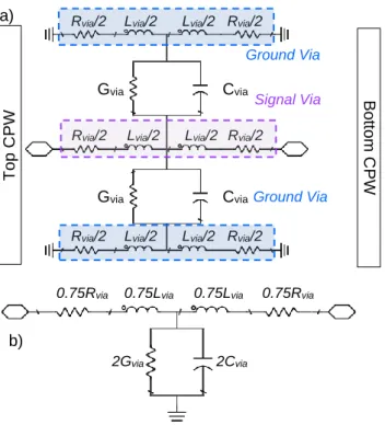
Figure 28 – a) Physical model for the transition with GSG vias, and b) Equivalent compact “T” model. ... 48 Figure 29 – Measurement of the direct coupling between via transition spaced of 57 µm in a structure without the bottom CPW (replaced by an open circuit) with the same dimensions as Via 1b. The inset shows the structure during measurement. ... 49
Figure 30 – In a) resistance and in b) inductance of solid copper via and copper nanowire-via. ... 53
Figure 31 – 2-D simulation of a nanowire-via at different frequencies showing the skin effect in nanowire-vias. The dots are the cross section of each nanowire. The red and blue dots indicate high and low current densities, respectively. In a) a square nanowire-via simulated in Maxwell and in b) a circular nanowire-nanowire-via in MATLAB using the matrix approach. The skin-effect is observed in both cases ... 54
Figure 32 – In a) resistance and in b) inductance vs. frequency of a nanowire-via and a solid via with metal conductance multiplied by the nanowires density. ... 55
Figure 33 – Measured and modeled S-parameters of the structure with vias (Via 2 and Via 3) presented in Figure 23, with L1 = 250 µm. ... 57
Figure 34 – Modeled S-parameters of each single via transition. ... 58 Figure 35 – Illustration of a 5-turns inductor using nanowire-vias with dimensions. In a) top view, in b) front view. ... 61
Figure 36 – The fabricated membrane with the 3-D inductors. In detail a 10-turns (left) and a 3-turns (right) inductor. ... 62
Figure 37 – Steps of the 3-D solenoid inductors with nanowire-vias fabrication process.. ... 62
Figure 38 – Picture of a fabricated 3-turns 3-D inductor under measurement. ... 63 Figure 39 – Extracted inductance and Q-factor of the measured (full line) and simulated (dashed line) inductors. ... 64
Figure 41 – Results extracted from the measured 3-D inductors (full line) and from the ADS/Momentum simulation of the 3-D inductors (dashed line). The image features the
extracted inductance and extracted quality factor. ... 66
Figure 42 – “T” Model utilized for the 3-D inductors. ... 67
Figure 43 – Steps for simplifying the electrical model derived from a physical interpretation of the 3-D solenoid structure... 68
Figure 44 – Ls extraction from measurements and simulations, versus the number of turns for different ground plane configurations. ... 69
Figure 45 – S-parameters measured results (full line) and the model utilized for the inductors structures (dashed line). ... 70
Figure 46 – Results extracted from the measured 3-D inductors (full line) and from the modelling of the 3-D inductors (dashed line). In a) extracted Inductance and in b) Q-factor. ... 70
Figure 47 – The parameters 𝑳𝑺 and 𝑹𝒔 used in the model versus the number of turns for each inductor. ... 71
Figure 48 – In a), overview of the analyzed slow-wave microstrip line (SMS). In b) and c), visualization of the electrical and magnetic field lines, respectively, in a transversal section. Only half of the SMS line was considered, due to properties of symmetries. ... 76
Figure 49 – Schematic of a slow-wave microstrip line in PCB technology. ... 77
Figure 50 – Schematic of a slow-wave microstrip line in MnM technology. ... 78
Figure 51 – Topology of the distributed model of the SMS lines. ... 78
Figure 52 – Schematic top view of the metallic vias organization with pads. 𝒅/𝒅𝒑𝒂𝒅 are the vias/pads diameters, 𝒓/𝒓𝒑𝒂𝒅 their radii, 𝒆/𝒆𝒑𝒂𝒅 their pitches, respectively. ... 79
Figure 53 – Electric field lines representation for capacitance calculus for the SMS lines. The electric field lines that give the main part of the linear capacitance are included in an equivalent width 𝑾𝒆𝒒. ... 80
the ground plane with ellipsis semi-major axis h1. ... 81
Figure 55 – Proposed linear capacitance for PCB technology a) and MnM technology b), respectively. Comparison between 𝑪𝑺𝑴𝑺−𝒎𝒆𝒂𝒔𝒖𝒓𝒆𝒅 extracted from measurements, 𝑪𝒎𝒊𝒄𝒓𝒐𝒔𝒕𝒓𝒊𝒑 calculated from [50] and proposed capacitance 𝑪𝑺𝑴𝑺. ... 84 Figure 56 – Magnetic field and corresponding inductance for a) microstrip with substrate thickness 𝒉𝟏, b) microstrip with substrate thickness 𝒉𝟏+ 𝒉𝟐. In c) is illustrated the flux difference between a) and b), and in d) is illustrated the magnetic flux of the SMS line with metallic vias and total substrate thickness 𝒉𝟏+ 𝒉𝟐. ... 86 Figure 57 – Comparison between the inductance of classical microstrip lines 𝑳𝒎𝒊𝒄𝒓𝒐𝒔𝒕𝒓𝒊𝒑 (red line), the proposed inductance 𝑳𝑺𝑴𝑺 (black line), and the inductance extracted from measurements of fabricated SMS lines in PCB technology 𝑳𝑺𝑴𝑺−𝒎𝒆𝒂𝒔𝒖𝒓𝒆𝒅 (blue squares). ... 87
Figure 58 – SMS line linear inductance 𝑳𝑺𝑴𝑺 calculated from proposed model for the metallic-nanowire-filled membrane technology (black line), compared to the inductance 𝑳𝒎𝒊𝒄𝒓𝒐𝒔𝒕𝒓𝒊𝒑 of a classical microstrip line with substrate height 𝒉𝟏 + 𝒉𝟐 extracted from [50] (red line), and the inductance 𝑳𝑺𝑴𝑺−𝒎𝒆𝒂𝒔𝒖𝒓𝒆𝒅 extracted from measurements (blue squares). ... 88
Figure 59 – SMS line top view with the region with size 𝑾 ∗ ∆𝒛 for the calculi of 𝑴𝒊𝒋. ... 90 Figure 60 – Comparison between the 𝜺𝒓𝒆𝒇𝒇 extracted from measurements and extracted from the model with and without the mutual coupling between the inductance representing the nanowires. ... 90
Figure 61 – Fabricated SMS line in PCB technology. Top and bottom views of a 10-mm long and 400-µm wide strip, with grounded CPW feeding lines... 92
Figure 62 – Fabricated SMS line in MnM technology. Top view of a 500-µm long and 92.75-µm wide strip, with GSG measurement pads (with interconnected grounds). . 92
measurements for the PCB technology. ... 94
Figure 64 – Characteristic impedance 𝒁𝟎, attenuation constant 𝜶, relative effective dielectric constant 𝜺𝒓𝒆𝒇𝒇 extracted from S-parameters model, simulation and measurements for the MnM technology. ... 96
work. ... 23
Table 2 – CPW and vias dimensions in µm. ... 46
Table 3 – Parameters for the Via Model. ... 56
Table 4 – Comparison of existing via technologies for mm-wave applications. ... 58
Table 5 – Parameters for the inductor model. ... 71
1 TECHNOLOGY DESCRIPTION AND CHARACTERIZATION ... 20
1.1 INTRODUCTION ... 20
1.2 FABRICATION PROCESS OF CIRCUITS ON THE MNMSUBSTRATE... 22
1.2.1 Former fabrication process ... 22
1.2.2 Fabrication Process Optimization ... 25
1.3 MEMBRANE CHARACTERIZATION ... 31
1.3.1 Electrical characterization using open-ended stub... 32
1.3.2 Electrical characterization using a filter ... 36
1.3.3 Summary of membrane characterization ... 39
1.4 SUMMARY ... 40
2 VIAS ON THE MNM SUBSTRATE ... 41
2.1 INTRODUCTION ... 41
2.2 NANOWIRE-VIAS TRANSITIONS ... 42
2.2.1 Fabrication Process ... 44
2.2.2 Characterization up to 110 GHz ... 45
2.2.3 Electrical Model ... 47
2.2.3.1 Analytical Inductance calculation ... 49
2.2.3.2 Inductance and resistance calculation in a matrix format ... 50
2.2.3.3 Rvia, Gvia, Cvia calculation and model validation ... 56
2.2.4 Comparison to the state-of-the-art ... 57
2.2.5 Summary ... 59 2.3 3-D SOLENOID INDUCTOR ... 59 2.3.1 Introduction ... 59 2.3.2 Design ... 60 2.3.3 Fabrication process ... 62 2.3.4 Characterization ... 63 2.3.5 Electrical Model ... 66
2.4 CHAPTER SUMMARY ... 73
3 SLOW-WAVE MICROSTRIP TRANSMISSION LINES ... 74
3.1 INTRODUCTION ... 74
3.2 SLOW-WAVE PRINCIPLE ... 75
3.3 ELECTRICAL MODEL ... 78
3.3.1 Linear capacitance 𝑪𝑺𝑴𝑺 ... 80
3.3.2 SMS line inductance 𝑳𝑺𝑴𝑺 ... 84
3.3.2.1 PCB technology ... 85
3.3.2.2 MnM technology ... 87
3.3.3 Metallic vias inductance 𝑳𝒗𝒊𝒂 and mutal 𝑴𝒊𝒋 ... 88
3.3.4 Metallic vias resistance 𝑹𝒗𝒊𝒂 ... 90
3.3.5 Linear strip resistance 𝑹 ... 90
3.3.6 Linear conductance 𝑮 ... 91 3.4 MODEL VALIDATION ... 91 3.4.1 PCB technology results ... 93 3.4.2 MnM technology results ... 95 3.5 DISCUSSION ... 96 3.6 SUMMARY ... 97 4 CONCLUSION... 98 REFERENCES ... 100
INTRODUCTION
From a consumer market point of view, devices must have low-cost, low power consumption and small dimensions. At mm-wave frequencies, i.e. from 30 GHz to 300 GHz, with the reduced size of distributed passive devices based on transmission lines, their on-chip integration with active circuits is possible, but they still occupy a large surface area of advanced CMOS technologies necessary at mm-wave frequencies, increasing costs prohibitively. Moreover, only mm-wave passive circuits (couplers, baluns, filters, etc.) with poor quality factor can be realized in standard CMOS/BiCMOS technologies, due to the very small thickness of the back-end-of-line (BEOL). The alternative solution is to fabricate the passive devices on a low-cost interposer with good RF performance. In that case, the active circuits would be fabricated on the most appropriate technology and integrated onto the interposer.
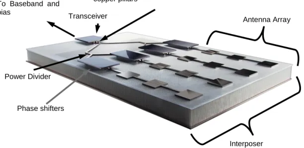
In the last ten years, much effort has been put forth to develop platforms where CMOS chips and/or MEMS, optical links, etc., are integrated onto interposers [1], [2]. An interposer is a platform similar to a PCB, optimized for a digital and/or radio frequency (RF) role. A range of integrated circuits (ICs) in different technologies can be integrated into the interposer, with its function to provide a platform with excellent performance for signal interconnection between different ICs and circuits. This is achieved using a good dielectric substrate as the interposer that has a good redistribution layer and through-substrate-vias (TSVs). A view of the general capacities of an interposer is shown in Figure 1.
Figure 1 – Example of general applications of an interposer.
A good interposer for mm-wave applications must have redistribution layers with high quality transmission lines, TSVs with good performance, among passive devices as inductors, transformers, couplers, antennas, interconnection posts, among others. In that context, the work presented in this thesis focuses on an interposer for mm-wave applications. A typical application of the mm-wave interposer that has been considered in this work is described in Figure 2, where a transmission/reception chain is shown. A baseband signal is connected to a transceiver, transferred to the interposer with interconnection posts, with TSVs connecting the baseband signal from the bottom layer to the transceiver on top, following with power dividers and phase shifters feeding an antenna array.
Figure 2 – Example of a mm-wave interposer, depicting a transmission/reception chain.
Interposers were reported in the literature using different materials such as glass [1], silicon [2], high resistivity silicon [3], liquid crystal polymer [4], among others [5].
This work helps to develop passives devices in a new interposer substrate called metallic nanowire-filled membrane (MnM) [6]. This interposer is an anodic alumina
oxide (AAO) membrane that has well-organized nanopores, where metallic copper nanowires can be grown inside, making it easier to have nanowire-via TSVs with good performance [7], [8]. The development of nanowire-vias makes it possible to have 3-D interconnections and circuits (for instance 3-D inductors). Apart from that, a wide range of transmission lines with a wide range of characteristic impedance and effective
Interposer
Antenna Array
Phase shifters To Baseband and bias
CPW to µstrip transition with vias and copper pillars
Power Divider
dielectric constant can be fabricated such as standard microstrip lines [6], coplanar waveguides (CPW) [6], substrate integrated waveguides [9] and specially slow-wave microstrip lines (SMS) [10], [11]. This work helps to develop the MnM substrate
aiming on the fabrication process for passive circuits, substrate characterization, nanowire-vias, 3-D inductors and an electrical model for SMS lines.
The interposer technology is presented in chapter 1. The fabrication process for passive devices on the MnM-platform is carefully described. Then, all the improvements to allow the fabrication of high-performance nanowire-vias are discussed. Next, the mm-wave characterization of the MnM substrate using open-ended microstrip stubs is presented. The resonant frequency of these stubs is measured and modeled to obtain the substrate dielectric constant and tangent loss. The characteristics of the substrate is then verified with the design and measurement of a filter based on short-ended microstrip stubs.
In chapter 2, nanowire-via transitions and 3-D inductors are studied at mm-waves. The nanowire-via transition uses coplanar waveguides (CPWs) to connect the top to the bottom of the MnM substrate. A simple lumped-element model is derived for the transition. State-of-the-art performance is obtained for the vias insertion loss. Next, the nanowire-via itself is mathematically modelled to help future designers. Then, based on the modeled developed for the vias, compact 3-D inductors are designed, fabricated measured and analyzed, and a lumped-element model related to the physical layout is derived for these structures.
In chapter 3, a distributed model for the SMS line on the MnM substrate is presented. The model is based on a classical RLGC transmission line model, and because of the nanowires, a resistance, inductance and magnetic mutual coupling inductance are added. The same model is applied to a transmission line on PCB technology that have the same configuration as the SMS lines on the MnM substrate. A good agreement between measurements and the model simulations is obtained for both the MnM and the PCB technologies.
1
TECHNOLOGY DESCRIPTION AND CHARACTERIZATION
1.1 Introduction
The MnM (Metallic-nanowire-filled-Membrane) is an alumina substrate obtained through electrochemical oxidation of aluminum in specified anodization voltages, as presented in [12]. The membrane is referred on the literature as anodic alumina oxide – AAO. In the anodization process several nanopores organized with different geometric parameters (pore diameter and interpore distance) are created as shown in Figure 3. Different acids can be used in the formation process such as oxalic acid, sulfuric acid or phosphoric acid with an electric potential interval used for each solution. In this way, this technology is versatile, since the geometric parameters can be adjusted on the substrate fabrication depending on the solution used and the electrical potential, and there is not a fixed size limit for the sample.
Figure 3 – Nanopores in a membrane with 40 nm pore diameter.
Source: InRedox – Application Note: “Are the Two Sides of Isotropic AAO Identical?”.
This membrane is used as a template for copper nanowire growth inside the pores, which is the greatest difference when comparing to other mm-wave interposers, such as low temperature co-fired ceramic (LTCC), glass, silicon, liquid crystal polymer (LCP) and others. Until the beginning of this work, the MnM substrate has been used to fabricate only slow-wave transmission lines [10], [11] as shown in the next section.
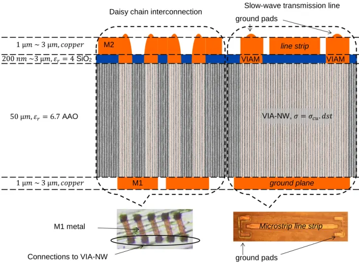
The MnM interposer technology can be seen in Figure 4 with all possible layers. From the bottom to the top of the substrate, there is a copper layer, M1, used as ground plane for microstrip lines. M1 is also the base layer for nanowire growth. Then, there is the nanoporous membrane, with air-filled or copper-filled (VIA-NW) nanopores,
having pore area density 𝑑𝑠𝑡. On the surface, there is a dielectric oxide layer composed of silicon dioxide (SiO2), and the top copper layer (M2). The connection of M2 with the VIA-NW is done with selective removal of the SiO2 layer, forming a connection called VIAM. All the thicknesses and characteristics of the different layers are given in Figure 4.
Figure 4 – Technology cross section of the MnM interposer.
Based on the MnM technology illustrated in Figure 4, a family of different passive circuits can be fabricated. The left part of Figure 4 shows an example of interconnection where M1 and M2 are connected through VIAM and VIA-NW. On the right part of Figure 4 there is an example of cross-section view of a slow-wave microstrip line, where M2 is used for the signal and M1 for the ground plane. The signal strip is separated from the nanowires (VIA-NW) by the SiO2 layer, creating the slow-wave effect that will be explained in Chapter 3. For measurement, coplanar (GSG) probes
ground plane line strip M2 M1 VIAM 200 𝑛𝑚 ~3 µ𝑚, 𝜀𝑟= 4 SiO2 50 µ𝑚, 𝜀𝑟= 6.7 AAO 1 µ𝑚 ~ 3 µ𝑚, 𝑐𝑜𝑝𝑝𝑒𝑟 1 µ𝑚 ~ 3 µ𝑚, 𝑐𝑜𝑝𝑝𝑒𝑟 VIA-NW, 𝜎 = 𝜎𝑐𝑢. 𝑑𝑠𝑡 Slow-wave transmission line ground pads
VIAM Daisy chain interconnection
ground pads
Microstrip line strip
M1 metal
are normally used and the VIA-NW and VIAM are to connect the ground pads to the ground plane.
The chapter is organized as follows to completely describe the technology. In section 1.2 the fabrication process of structures on top of the MnM substrate is presented, first with the process used before this work shown in section 1.2.1, followed by the optimizations performed in section 1.2.2. In section 1.3 a high frequency electrical characterization of the MnM substrate is performed, using open-ended microstrip stubs (section 1.3.1) followed by a verification with the design and measurement of a filter at mm-wave frequencies, and based on short-ended microstrip stubs (section 1.3.2). Section 1.4 presents a summary of the points presented in this chapter.
1.2 Fabrication process of circuits on the MnM Substrate
In this section, the fabrication process for circuits on the membrane is presented. First, the fabrication process used before this work is presented in section 1.2.1. This fabrication process allowed only slow-wave microstrip lines with nanowires to be fabricated all over the membrane, and only in one type of membrane (a 50-µm-thick membrane from Synkera with 55-nm pore diameter), since this combination of thickness and pore diameter was the best for nanowire growth. In section 1.2.2, it is shown how the fabrication process was modified to allow a range of different circuit with different layouts to be fabricated in a single run, and in membranes with different pore diameters.
1.2.1 Former fabrication process
The fabrication process for making circuits using 50-µm-thick AAO membranes before the start of this work is described in Table 1. Using those steps, it was not possible to grow nanowires selectively on the membrane, which limited the types of circuits that were possible to fabricate.
Table 1 – Fabrication process for circuits on the MnM substrate before the start of this work.
Steps Membrane visualization Process/Technique Conditions
1 Membrane cleaning Boiling (5 minutes)
for each solvent
1 – Trichloroethylene 2 – Acetone 3 – Isopropyl alcohol 2
Copper deposition on bottom of the membrane (30 nm thickness)
Sputtering 70 W; 2 mTorr; 1m30s
3 Bottom copper thickening Electroplating
Acid copper sulfate solution from EPI and copper electrodes. 30 min with 100 mA
4
Nanowire growth through the nanopores until the formation of a copper film on the top surface
Electroplating
Same solution as last step with 60 mA ∼ 100 mA (The membrane is immersed in water with developer in a vacuum chamber to lower the surface tensions and fill the nanopores with water)
5
Copper removal from the top and bottom leaving only the nanowires
Mechanical removal with a tweezer
The border of the membrane is broken to get the copper layer from top and bottom
6 Membrane cleaning Boiling (5 minutes)
for each solvent
1 – Trichloroethylene 2 – Acetone 3 – Isopropyl alcohol
7 SiO2 deposition on the top
layer PECVD 75 sccm – N2O 30 sccm – SiH4 200 W, 320 °C 8 Titanium deposition (20 ηm) and copper (30 ηm) on the bottom layer for the ground plane
Sputtering
Titanium:100W 2 mTorr;
1 min
Copper: 70W; 2 mTorr;
1 min 30 s
9 Bottom copper thickening Electroplating Same solution as step 4:
40 min 200 mA
10
Titanium deposition (20 ηm) and copper (30 ηm) on the bottom layer for the top surface – surface where the circuits are fabricated Sputtering Titanium:100W 2 mTorr; 1 min Copper: 70W; 2 mTorr; 1 min 30 s
11 Top copper thickening Electroplating Same solution as step 4:
40 min 200 mA
(continues in the next page)
(continuation of Table 1)
Steps Membrane visualization Process/Technique Conditions
12 Photolithography (mask) Thick photoresist –
3 to 4 µm
13 Top copper corrosion Wet etching
Chromium etching solution: perchloric acid and cerium ammonium nitrate
14 Photoresist removal Boiling (5 min) Acetone. Afterwards
cleaning with DI water
This process has been improved in order to fabricate other types of structures that need nanowires only in specific parts of the membrane such as TSVs, making a good electrical contact between the bottom and the top of the membrane; specially to make the fabrication process more reliable. The motivations for changes are listed below, and addressed in section 1.2.2.
In step 5, the copper is removed from the top and bottom of the membrane. The top copper is removed to allow the deposition of the SiO2 layer. The bottom is removed only to prevent the mechanical deformation due to the mismatch in thermal coefficient during the SiO2 deposition step (Table 1; step 7). The deposition is executed using the plasma-enhanced chemical vapor deposition (PECVD) technique, which requires temperatures around 320 ºC. Having a membrane with copper on one side and depositing SiO2 on the other side, leads to a considerable mechanical stress on the membrane, caused by different thermal expansion coefficients between the copper, the alumina membrane and SiO2. For some circuits it is important to maintain the copper layer to ensure a good electrical contact between the nanowires and the copper on one side.
Also in step 5, the top copper grown after the nanowires is removed with tweezers that is only possible since it is a contiguous layer. This removal technique is not suitable for processes with nanowires in specific regions of the membrane.
The definition of structures on the copper using a corrosion method (Table 1; steps 11-13) gives a significant difference in thickness between the border and the center of the membrane; a better thickness control is needed.
1.2.2 Fabrication Process Optimization
The first change in the fabrication process was in the SiO2 deposition technique (Table 1; step 7) from PECVD to radiofrequency (RF) magnetron reactive sputtering. With the sputtering technique it is possible to deposit SiO2 at lower temperatures (about 100 ºC), which allows the deposition on the membrane with copper in one face with reduced mechanical stress.
The development of the selective nanowire growth was necessary for the realization of nanowire-vias (VIA-NM). With this technique, it is possible to fabricate slow-wave microstrip lines, standard microstrip lines, CPW, nanowire-vias on the same substrate and in the same fabrication run. For this selective growth, two possibilities for masking the membrane nanopores were proposed and explored. The first one consists of a SiO2 mask on the top of the membrane, and copper on the bottom, with nanopores exposed only in selected areas, as shown in Figure 5 a). The second also uses SiO2 as mask, with copper on top of this mask, leaving all nanopores exposed, as shown in Figure 5 b).
Figure 5 – Two masking possibilities for growing nanowires inside the membrane, in a) with the SiO2 layer on the top and in b) with the SiO2 layer on the bottom surface.
Looking at the solution proposed in Figure 5 a) the fabrication procedure would be to first deposit the SiO2 layer on top followed by the bottom copper layer, and then etching the SiO2. The solution proposed in Figure 5 b) is fabricated by first depositing the bottom SiO2 layer, etching it and then depositing the copper layer below. The latter fabrication process implies that a SiO2 wet etching solution can penetrate through the nanowires from the exposed surface, attacking the layer from both sides and diminishing the mask adherence and resolution. In the former fabrication process, all
a) b)
Top Conductor SiO2 Membrane
the nanopores are covered leading to a more controlled SiO2 etching, being it the main reason for choosing the Figure 5 a) masking solution.
Initial attempts to selectively grow nanowires were performed using only the sputtered SiO2 as mask, as will be explained later, not being successful and often resulting in no nanowire growth or growth all over the membrane, as shown in Figure 6. Since it was suspected that the masking choice was not the only problem, further investigations were performed on all process parts involved, the SiO2 etching procedure, the deposited SiO2 characteristics, and the electrodeposition solution employed and its biasing.
Figure 6 – Example of unsuccessful selective nanowire growth, with nanowires all over the membrane in copper color, whereas the designated regions are inside the geometric forms.
For etching the mask and exposing the nanopores, a buffered oxide etch (BOE) solution is used. A SiO2 layer deposited on a silicon substrate on the same sputtering run is used to approximate the etching time. After several fabrication tests, it was observed that the time needed to properly expose the nanopores to have a good nanowire growth is about three to four times higher than the time for the SiO2 on the silicon. This implies that the mask is etched an extended time after defining the exposed regions, diminishing its resolution. This might be caused by SiO2 deposition inside the membrane nanopores. To improve the overall mask resolution, the initial
1-µm-thick mask used in the initial fabrications was reduced to about 300 nm in
Further investigations on the SiO2 characteristics showed that the initial recipe employed for its sputtered deposition formed an oxide with inner tensions, as shown in Figure 7. This characteristic can create cracks inside the film, making it porous and leading to nanowire growth outside designed areas. To find a more suitable deposition recipe, several depositions were done and their characteristics analyzed. As a result, the deposition gases flow ratio were changed and to further avoid thermal stress during the process, the substrate temperature is now kept low, with successive 10-minutes spaced depositions. Even with this optimized SiO2 mask, as a preventive measure, the photoresist used for its etching is left as a second barrier for the nanowire growth mask.
Figure 7 – SiO2 on top of a silicon substrate where a film with higher inner tensions and stressed
corners is shown.
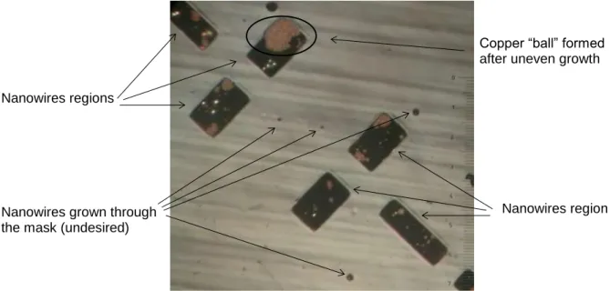
The electrodeposition solution from EPI (https://www.epi.com/) with DC current was used successfully for the nanowire growth in the entire membrane (Table 1; step 4). However, in the selective case, the growth was uneven and disorganized. In some areas, no nanowire growth was observed at all with either of the masking possibilities shown in Figure 5. In other areas, the growth was much faster, leading to the formation of copper “balls” and unbalanced growth between nanowire regions, as is exemplified in Figure 8.
Stressed corners on the SiO2
Figure 8 – Membrane on the microscope after nanowire growth. The dark brown regions are areas stipulated for nanowire, with disorganized growth. Some regions had a faster growth than others, forming copper “balls”.
Other electrodeposition solutions for the nanowire growth were analyzed, with a solution that uses a periodic pulse reverse (PPR) biasing appearing to be the best option. The PPR bias leads to a better copper ions distribution over the sample and to a uniform copper growth. The solution “Macuspec PPR 100,” proposed by the company MacDermid was chosen.
Figure 9 – Example of periodic pulse reverse (PPR) current signal used for biasing the electrodeposition solution for nanowire growth on the membrane.
With all of these optimizations, selective copper nanowire growth was made possible. Figure 10 shows how a good nanowire growth is expected to look after the electrodeposition process, in contrast with Figure 6 before process optimization. In Figure 10, the orange regions are regions with copper grown after the growth surpassed the nanopores, the red region is a photoresist layer on top of a SiO2 mask, serving as an additional protection layer to the mask.
Copper “ball” formed after uneven growth Nanowires regions
Nanowires region Nanowires grown through
the mask (undesired)
I (current)
Figure 10 – Nanowire growth after all optimizations. In red the photoresist additional layer on top of the SiO2 mask, and in orange the excess copper after the nanowires growth in the delimited
regions.
Following with the fabrication process optimization, a polishing machine (Tegramin-25 from Struers) is now employed for removing the excess copper after the nanowire growth, instead of breaking a small edge of the membrane and removing it mechanically with help of a tweezer as in the step 5 from Table 1. This technique permits to remove the natural roughness of the membrane, resulting in lower signal losses in designed circuits.
The definition of structures on the copper layer is done using a corrosion method. First, the copper was grown to the final thickness and then etched. The current density of the growth was not well controlled, leading to a thickness difference between the border and the center of the membrane. A DC and PPR electroplating solution from MacDermid were explored and a better current density control was performed, resulting in either solutions being acceptable. For convenience, the PPR solution is used as it is the same for growing nanowires. The wet etching used before was a chromium etching solution, not specific to copper, leading often to roughness on the structures edge. An etching solution specific to copper from AlfaCleaner is now employed, with a characterized typical 5 µm overetching. Masks for the structures using this corrosion method includes 5 µm more on each structure side to overcome the overetching, leading to a minimal strip width of 15 µm.
The optimizations described until now made the fabrication process more reliable. The yield of success for nanowire-vias fabrication was increased. Membranes with different pores sizes can now be used, such as 80-nm and 160-nm. Nevertheless, membranes with around 55-nm pore diameter present the best yield for nanowire
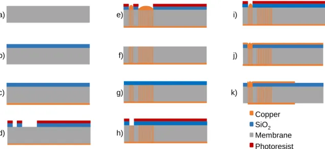
growth. Figure 11 shows the general fabrication process after all proposed optimizations. This general process is adapted to each membrane fabrication, as steps can be added or removed, as they are needed.
Figure 11 – Optimized fabrication process employed for fabricating circuits on the membrane as nanowire-vias and circuits with slow-wave transmission lines. This general process is adapted to each fabrication.
The general fabrication process can be described by the steps below.
a) A membrane chosen in height and pore dimension, always 1-inch-diameter wafers, and cleaning 10 minutes in boiling trichloroethylene, followed by acetone and isopropyl alcohol;
b) SiO2 mask deposition by RF sputtering (about 330 nm): 2 mTorr, Ar 70 sccm, O2 30 sccm and plasma power of 150 W, with deposition rate of 16 nm/min;
c) M1 copper deposition, first a Ti seed deposition for adherence using RF sputtering: 2 mTorr, Ar 10 sccm, 100 W, 20s is done, followed by copper seed deposition using RF Sputtering: 2 mTorr, Ar 10 sccm, 70 W, 10 minutes. The copper seed layer is then thickened using the “Macuspec PPR 100” electrodeposition solution with 25 mA DC current (about 490 mA/dm²), 20 min giving 2 µm copper thickness;
d) Photoresist is coated and exposed/developed. The SiO2 mask layer is opened in a BOE (1 part HF 49% in water, 6 parts NH4F 40% in water) solution for about 4 minutes; a) e) i) b) f) j) c) g) k) d) h) Photoresist Copper SiO2 Membrane
e) Nanowires (VIA-NW) are grown in the “Macuspec PPR 100” solution, using a periodic pulsed current with 20 ms positive current and 1 ms negative current. The positive current density is about 300 to 700 mA/dm² adapted to each mask used. The negative current density is about 3 to 4 times the positive current. The photoresist is left as an additional protection layer to the SiO2 mask,for the nanowire growth;
f) The photoresist is removed on acetone, followed by acetic acid. The membrane is then polished to remove the excess copper, and then fine polished to remove the roughness. The membrane is cleaned for 10 minutes in deionized water;
g) SiO2 depositionfor slow-wave transmission lines as in item b). The deposition time depends on the desired thickness, usually 1 µm, with successive 10-minutes spaced depositions to not raise the substrate temperature;
h) Photoresist is coated and exposed/developed for masking the SiO2. The oxide is opened using BOE, to expose the nanowire-vias region. The corrosion time depends on its thickness, and is estimated by SiO2 deposited on the same run in silicon samples. The photoresist is left as an additional protection layer for the next step. Mask alignment is performed with alignment structures;
i) Copper is electrodeposited to create an electrical contact between the nanowire-vias and the top copper layer (VIAM layer);
j) The photoresist is removed and seed copper for layer M2 is deposited and thickened as in step c), for the top surface;
k) The strips in layers M1 and M2 are defined in this step using a photoresist mask and etch using the solution “SuperEtch” from the “Alfacleaner” company for 30 s at 35°C. Over-etching is about 5 µm. Afterwards the titanium is removed using a 20:1 water HF solution for 20 s.
1.3 Membrane characterization
Electrical characterization of the membrane without nanowires, i.e. with the nanopores “filled” with air, is necessary to the design of passive devices on the membrane, such as microstrip lines, coplanar waveguides (CPWs), cross-overs,
among others. From the electrical characterization is extracted the relative dielectric constant 𝜀𝑟 and dielectric losses, represented by the loss tangent tan 𝛿, of the substrate. First, an electrical characterization using microstrip open stubs is performed. A second characterization is done using a filter composed of microstrip lines with short-ended microstrip stubs also, as filter behavior is highly dependent on the substrate characteristics. Since the membrane presents vertical pores, it is “tough” that it has some anisotropy, i.e., the vertical 𝜀𝑟 is different from the horizontal one. The two characterization methods employing microstrip lines having a mainly vertical electrical field, they give us mainly the vertical 𝜀𝑟.
1.3.1 Electrical characterization using open-ended stub
Quarter wavelength (𝜆/4) open-ended stubs in microstrip technology was first proposed in [13] for substrate electrical characterization, where the stubs form a “T” with a thru-line, as shown in Figure 12. This “T-pattern” gives a simple resonant structure. From its resonant frequency and 3-dB bandwidth, the electrical characteristics of the substrate can be extracted. In [13] equations are used to extract the relative dielectric constant 𝜀𝑟 of the substrate and losses represented by tan 𝛿.
Figure 12 –“T” open-ended stubs topology used for electrical characterization.
In this section, the same method is employed for the membrane characterization, and the results are compared with simulations done in the 2.5-D electromagnetic (EM) simulator from Keysight ADS/Momentum.
50-μm-thick anodic aluminum oxide (AAO) membranes from Synkera are employed in this characterization, having 55-nm pore diameter and interpore distance of 143 nm. Those have initially shown the best results for nanowires growth, and are employed for many of the circuits developed in this work. As Synkera stopped
Input Output
fabricating AAO membranes, during the course of this work, the provider was changed to InRedox, with the InRedox membranes having similar electric characteristics.
Five microstrip lines with 𝜆/4 open stubs were fabricated, measured and analyzed. Each fabricated microstrip open-ended stub has a different length, so that the structures resonate at different frequencies. The fabricated lengths 𝐿 were 640 μm, 530 μm, 459 μm, 406 μm and 360 μm, respectively. Some fabricated structures are shown in Figure 13.
Figure 13 – Microstrip lines with open stubs fabricated for electrical characterization. In a) structure with a 640 μm long stub, in b) with 459 μm and in c) 360 μm. In orange the microstrip lines and in light blue the membrane. The blue color is due the SiO2 layer.
The structures features a 0.3-μm-thick SiO2 layer between the membrane and the top metallization, used to mask the nanopores and allow the growth of nanowires only for the resistive probe contact pads to the lower ground plane. As this layer is very thin, it does not interfere with the overall electrical characterization. The transversal section of the structures can be seen in Figure 14 a). The fabricated structures were measured with the help of a microscope and the layout reproduced in the ADS/Momentum EM simulator. In Figure 14 b), we have the layout for a structure with 640 μm long stub reproduced.
500 μm a)
b) c)
Figure 14 – In a) the transversal section of the open-ended microstrip stubs and in b) layout of microstrip line with 640 μm long stub. All structures were measured and the corresponding
layout reproduced.
In the ADS/Momentum software, the membrane’s parameters 𝜀𝑟 and tan 𝛿 were set as variables, for fitting between measured and simulated S-parameters.
Using a co-simulation between the ADS/Schematics electrical simulator and Momentum simulator, the membrane’s parameters were varied. In a first step, tan 𝛿 was set fixed and equal to 0.01 at 60 GHz and 𝜀𝑟 was varied. In Figure 15 it is shown the measured 𝑆21 for the structure with 640-μm long stub that resonates at 54.4 GHz and simulations for this structure varying 𝜀𝑟. From the same Figure 15 it can be seen that with 𝜀𝑟 = 6.7 the simulated resonance frequency agrees well with the measured one.
Figure 15 – Membrane simulation 𝜺𝒓 variation and measurement with stub resonating at
54.4 GHz. Co-simulated with ADS/Momentum and ADS/Schematics. Looking at the results 𝜺𝒓= 𝟔. 𝟕 better agrees with the measurement.
-40 -30 -20 -10 45 50 55 60 65 S21 (dB ) Frequency (GHz) εr=6.5 εr=6.6 εr=6.7 εr=6.8 εr=6.9 Measured 50 µm 0.3 µm Not to scale
Nanowire-via (top view) Copper
SiO2 Membrane
500 μm
Fixing 𝜀𝑟 = 6.7, tan 𝛿 is then varied in the same manner, with results shown in Figure 16. tan 𝛿 = 0.05 at 60 GHz leads to a good agreement between measurement and simulation results.
Figure 16 – Variation of 𝐭𝐚𝐧 𝜹 at 60 GHz for 𝜺𝒓= 𝟔. 𝟕 in comparison with the measured structure
with ressonance at 54.4 GHz.
To verify that the extracted parameters 𝜀𝑟= 6.7 and tan 𝛿 = 0.05 at 60 GHz are consistent in frequency, all other microstrip structures with open stubs were simulated using those values with Momentum. In Figure 17 it can be seen the measured and simulated 𝑆21 for all structures. The structures with stubs length 640 μm, 530 μm, 459 μm, 406 μm and 360 μm resonate at 54.4 GHz, 65.6 GHz, 76.1 GHz, 85.5 GHz and 95.3 GHz respectively. Up to 85.5 GHz, the agreement between simulation and measurement results is good. At higher frequency, with the structure that resonates at 95.3 GHz, a deviation between simulation and measurement results occurs.
Figure 17 – Measured and simulated S21 results for all microstrip structures with open stubs
using extracted parameters 𝜺𝒓= 𝟔. 𝟕 and 𝐭𝐚𝐧 𝜹 = 𝟎. 𝟎𝟓 at 60 GHz. Solid lines are measured
results and dashed lines are simulated one.
-40 -30 -20 -10 45 50 55 60 65 S21 (dB ) Frequency (GHz) tg δ=0.02 tg δ=0.037 tg δ=0.05 tg δ=0.069 tg δ=0.126 Measured -40 -30 -20 -10 0 0 10 20 30 40 50 60 70 80 90 100 110 S21 (dB ) Frequency (GHz) 54.4 GHz 65.6 GHz 76.1 GHz 85.5 GHz 95.3 GHz Measurement Simulation
For the structure that resonates at 95.3 GHz, the same procedure as before was employed to find the 𝜀𝑟 and tan 𝛿. It was found that 𝜀𝑟 = 7 and tan 𝛿 = 0.07, as show in Figure 18.
Figure 18 – Measured and simulated S21 results for structure resonating at 95.3 GHz using
extracted parameters 𝜺𝒓= 𝟕 and 𝐭𝐚𝐧 𝜹 = 𝟎, 𝟎𝟕.
From the simulations, we can see that up to 85.5 GHz, the electrical characteristics of the porous membrane without nanowires dos not change; it is 𝜀𝑟 = 6.7 and tan 𝛿 = 0.05, whereas at 95.3 GHz this value changes to 𝜀𝑟 = 7 and tan 𝛿 = 0.07. This means that the electrical characteristics of the combination of nanopores filled with air and alumina from the membrane may change at frequencies above 80 GHz. However, only one point was measured above 80 GHz. Hence, for applications clearly beyond 100 GHz, complementary characterization in this frequency range may be necessary.
1.3.2 Electrical characterization using a filter
The filter proposed in this section was designed to be a band-pass filter in Ka
band, from 27 GHz to 40 GHz, and rejection band with attenuation higher than 30 dB below 15 GHz and above 70 GHz. The filter was designed on ADS/Schematics. Initially an ideal filter was simulated with the Design Assistance tool. Afterwards, with the same specification, the DA_SBFilter smart component was used to implement the filter in microstrip technology, with short-ended stubs making use of nanowire-vias. The filter was simulated using a 50-µm-thick membrane with 55-nm nanopores diameter and 143-nm spacing between pores. The dielectric constant of 7.6 for the membrane without nanowires was employed. It is slightly different from the value extracted in section 1.3.1, these works being carried out in parallel, and 7.6 being the first
-40 -30 -20 -10 0 0 10 20 30 40 50 60 70 80 90 100 110 S21 (dB ) Frequency (GHz) 95.3 GHz – Measured 95.3 GHz – Simulated
approximation used of the nanoporous membrane dielectric constant. In Figure 19 it is shown the ideal filter simulated using the Design Assistance tool. It can be seen that spurious resonances appear between 60 GHz and 70 GHz, within the rejection band. The return loss is also quite poor in the passband. This is not really an issue since the filter was designed only for characterization purposes.
Figure 19 – Simulated ideal S-parameters from the proposed Ka band pass filter and a highlight
of the pass band.
The filter layout was generated using the DA_SBFilter smart component. Pads were added for measurement and vias to short-circuit the stubs. The layout used for fabrication is shown in Figure 20.
Figure 20 – Layout of the designed microstrip band-pass filter on the membrane with short-circuited stubs.
Several photos of the realized filter were taken using a microscope and the complete reconstructed photography is shown in Figure 21. The membrane surface
Frequency (GHz)
Frequency (GHz)
1000 μm Nanowire-via
Copper
roughness can be seen as diagonal lines, and since the membrane is translucent, the bottom ground plane can also be seen. In this fabrication, some parts of the ground plane had more adhesion to the membrane than others. On the parts of the figure where the ground plane is bright there was a good adhesion between the copper and the membrane.
Figure 21 – Fabricated band-pass filter.
The filter actual physical dimensions were measured using a microscope, and the filter was simulated with the measured dimensions with ADS/Momentum. The membrane’s relative dielectric constant 𝜀𝑟 and loss tangent tan 𝛿 were varied to obtain a good agreement between simulation and measurement results. Measured and simulated S-parameters are shown in Figure 22. From the measurement results, the filter presents a 3-dB pass-band from 26.43 GHz to 44.85 GHz, slightly higher than the
Ka band (27 GHz to 44 GHz). The insertion loss in the pass band is higher than 4 dB.
The simulation shown in Figure 22 was carried out after fitting measurement and simulation results with 𝜀𝑟= 7.1 and tan 𝛿 = 0.07.
Figure 22 – Measured and simulated S-parameters for the microstrip band-pass filter with short-circuited stubs. Highlighted the pass-band, from 26.43 GHz to 44.85 GHz, with insertion loss higher than 4 dB. -40 -36 -32 -28 -24 -20 -16 -12 -8 -4 0 0 10 20 30 40 50 60 70 80 90 100 S -p a ra m e te r (d B) Frequency (GHz) Simulated Measured S21 S11 26.43 GHz, -7.29 dB 44.85 GHz, -7.12 dB -16 -13 -10 -7 -4 0 10 20 30 40 50 60 70 80 90 100 S 2 1 ( d B ) Frequency (GHz) 1000 µm
1.3.3 Summary of membrane characterization
It was shown the electrical characterization of AAO membranes from Synkera, with 55-nm pore diameter and 143-nm interpore distance, using microstrip lines with open-ended stubs and using a microstrip filter. From the open-ended stubs, it was found that 𝜀𝑟 = 6.7 and tan 𝛿 = 0.05 extracted at 60 GHz is a good value up to at least 85.5 GHz. Above this frequency, the characteristics seem to change, and for a stub operating at 95.3 GHz the values of 𝜀𝑟= 7 and tan 𝛿 = 0.07 were found. From the filter, the found electrical characteristics were 𝜀𝑟= 7.1 and tan 𝛿 = 0.07. The different values found using the microstrip filter (𝜀𝑟 = 7.1 and tan 𝛿 = 0.07) as compared to the open-ended stubs over the same frequency range (𝜀𝑟 = 6.7 and tan 𝛿 = 0.05) can be due to process variations between the membrane’s fabrication. It can also be noted that the filter fabrication process did not have the best result, having the copper metal at the bottom not properly adhering to the membrane, in this way probably leading to higher losses. The electrical values extracted from the open-ended stubs method were considered as more reliable for those reasons. As will be shown through the results presented in this work, they also agree with other fabricated passive structures on the membrane. It should also be noted that the extracted 𝜀𝑟 from both methods is different from pure alumina (𝜀𝑟 in between 9.6 and 10), because of the influence of the air-filled nanopores.
This extraction was made using microstrip structures, so the electrical field is mainly oriented vertically in the membrane. If the electrical field is horizontal, as in coplanar waveguides (CPW), the dielectric constant may be different because of the vertical orientation of the air-filled nanopores. The dielectric loss represented by tan 𝛿 that was found is at least two orders of magnitude higher than the expected one for pure alumina. These higher losses are probably related to the formation process of the membrane, as it might happen that not all aluminum was anodized into alumina. Another manufacturer, InRedox, explains that if the fabricated membranes have an additional thermal treatment, the dielectric losses may be decreased.
1.4 Summary
This chapter presented the MnM technology, its fabrication process and its high frequency electrical characterization.
The fabrication process was optimized during this work. With the optimization, it is now possible to have a range of different circuits with different layouts on the same membrane, especially circuits using TSVs alongside circuits using slow-wave microstrips, as will be shown in the next chapters. In addition, the fabrication process is now more reliable, with a higher yield of structures in each fabrication.
The electrical characteristics of the MnM membrane without nanowires were extracted from two methods, using open-ended microstrip stubs and a microstrip based short-ended stubs filter. With this characterization, the membrane presents a relative dielectric constant 𝜀𝑟 = 6.7 and loss tangent tan 𝛿 = 0.05, up to at least 85 GHz.
In chapter 1, now that the fabrication process optimization made its fabrication possible, nanowire-vias are explored. Transitions and a 3-D solenoid inductor employing nanowire-vias as TSVs are presented, fabricated, measured and analyzed. In chapter 3, new slow-wave transmission lines fabricated after the fabrication process optimization are analyzed and a linear model is presented.
2
VIAS ON THE MNM SUBSTRATE
2.1 Introduction
High quality through-substrate-vias (TSVs) are fundamental for an mm-wave interposer. They act as a routing structure connecting the top and bottom parts of an interposer, enabling all sorts of passive circuits and complex structures to be fabricated. A good interposer should have TSVs with high performance, to assure good signal integrity and low attenuation, and with a small footprint, to have high-density interconnections.
In the literature, TSVs in interposers appear in silicon with limited performance because of the conductivity of the silicon (1-20 Ω cm), achieving 0.28 dB of loss at 60 GHz for one transition [14]. Vias in high resistivity silicon (HR-Si) present better performance because of the higher resistivity of the substrate, although this solution comes with increased costs. Via transitions in glass have been demonstrated with similar performance, e.g., 0.34 dB of loss per transition at 50 GHz [15]. In Liquid Crystal Polymer (LCP) technology, a loss of 1 dB per transition at 110 GHz was achieved [4].
In the mentioned technologies, the fabrication of vias involves special processes in order to “drill” the substrate. In Si and HR-Si, deep reactive-ion etching (DRIE) process is the main technique used for via etching. For filling the via, several processes can be used, such as electroplating copper from one side to another, depositing copper, tungsten, or nickel on its side, applying conductive paste or introducing wires magnetically [3]. In addition, a barrier layer is needed between the via and the substrate (Si or HR-Si), usually a layer of silicon dioxide is used [16]. When the DRIE process cannot etch the via up to the other side due to the aspect ratio limits, a final step of substrate thinning is needed in order to open the vias. This increases the fabrication cost, complexity and fabrication time. With this fabrication process, small vias with 3-µm diameter have been reported on a 50-µm-thick substrate, using an optimized process [17].
In glass interposers, to drill the vias, several fabrication processes have been investigated, such as DRIE, photochemical etching, sandblasting, electrical discharge and laser techniques. The laser techniques produce tapered vias with different