A DIGITAL TECHNIQUE FOR PRECISE MEASUREMENT
OF CAPACITOR DIFFERENCES, WITH APPLICATION
TO CAPACITIVE INTEGRATED SENSORS
by
Joseph T. Kung
Bachelor of Science, Electrical Engineering University of Illinois at Urbana-Champaign
(1985)
Submitted to the
Department of Electrical Engineering and Computer Science
In Partial Fulfillment of the RequirementsFor the Degree of
Master of Science
at the
Massachusetts Institute of Technology
June 1987(Massachusetts Institute of Technology
Signature of Author
Departme~/otl lectrical Engin g and Computer Science May 8, 1987 Certified by
Certified by
Accepted by
2U/' Hae-Seung Lee
Thesis Supervisor Roger T. Howe
•jsis
Supervisor Charman, Department F TECHNOLOGYTu JUL 0 8 1987 LI RAR'ES ..\>> Arthur C. SmithCommittee on Graduate Students
I At_ -
A-4 CIN11
Joseph T. Kung
Submitted to the Department of Electrical Engineering
and Computer Science on May 8, 1987 in partial
fulfillment of the requirements for the Degree of
Master of Science in Electrical Engineering and Computer Science
Abstract
'
'-:hnique for measurement of capacitor differences has been developed that has its origins in charge redistribution analog-to-digital converters. Effects of parasitic capacitance and MOS switch charge injection are canceled. The capacitance differ-ence can be obtained as a voltage in both digital and analog form with no additional circuitry needed. This makes it ideally suited for digital signal processing. Since the technique can be made relatively insensitive to parasitic capacitance, differences in small capacitances such as capacitive integrated sensors can be measured.
It is shown that measurements on 20 to 100 femtofarad capacitors are possible using this method. Effects of junction leakage, capacitor and transistor hysteresis, comparator offset, MOS switch charge injection, and voltage and temperature co-efficients are taken into account. Noise from the comparator, MOS switch, power supplies and clock feedthrough are considered as sources of error and dictate the minimum resolution.
Extensive measurements are made from test chips fabricated in 3 im CMOS technology. Detection of percent differences of less than 0.5% on 20 to 100 femto-farad capacitors has been successfully demonstrated.
Thesis Supervisors: Hae-Seung Lee and Roger T. Howe
3
Acknowledgments
During the course of this thesis, numerous colleagues and friends have helped me achieve the results of this work. In the MIT Microsystems Technology Laboratories, I would like to thank Jarvis Jacobs for helping me to understand the intricacies of our computer system, CAF (Computer Aided Fabrication), as well as the many stimulating conversations we have had; Vince McNeil for many interesting conver-sations on sensors; Jon Wade for insightful discussions on VLSI; Duane Boning for his software package GIRAPHE that helped create some of the graphs in this thesis; Ted Tewksbury for useful discussions on the self-calibration technique, his results on transistor hysteresis, and for the design of the CMOS op-amp; and finally, to my advisors, Hae-Seung Lee and Roger T. Howe. Without their knowledge, careful guidance, patience and support, this thesis would not be possible.
At MIT, I would like to thank Alice Twohig for making the administrative concerns at MIT an easier task to manage. She has made the EECS graduate office a very pleasant stop.
During the course of my life, I have been fortunate to have such a caring and loving family supporting me. This thesis is dedicated to them.
Support for this research was provided in part by the National Science Founda-tion under Contract No. ECS85-05145, by the Analog Consortium at MIT (Analog Devices, AT&T Bell Labs, General Electric, Digital Equipment Corporation, Texas Instruments), and in part by IBM through an IBM Faculty Development Award held by Roger T. Howe. MOSIS chip fabrication and other support has been pro-vided by DARPA under grant N00014-80-C-0622.
Contents
Abstract 2
Ackowledgements 3
List of Figures 7
List of Tables 8
List of Symbols and Acronyms 10
1 Introduction 13
2 Theoretical Background 19
2.1 Force Detection Methods ... 19
2.1.1 Piezoresistive Technique ... 20
2.1.2 Capacitive Technique . ... 22
2.2 Calibration Technique: Historical Origins ... 24
2.2.1 Charge Redistribution A/D Conversion . ... 25
2.2.2 Capacitance Mismatch Measurement in A/D Converters . . . 29
3 Self-Calibration Technique: Theory 33 3.1 Application to A/D Converters ... .. 33
3.2 Application to Measurement of Capacitive Differences ... 36
3.3 Non-Ideal Effects ... 39
3.3.1 Circuit Non-Idealities . ... 41
3.3.2 Component Non-Idealities . ... 53
3.3.3 Noise ... 59
3.4 Other Charge Injection Sources . ... . . 61
4 Capacitive Measurement System Design 63 4.1 Test Chip Design ... 63
4.2 Charge Injection Estimation ... 4.3 System Test Equipment ... 5 Experimental Results
5.1 Capacitive Difference Measurement Data . 5.2 Charge Injection and Offset Data ... 5.3 Discussion ...
6 Conclusions
6.1 Circuitry & Sensor Interfacing Issres ...
6.2 Comparison of Capacitance Measurement Techniques .
A Generality of Charge Redistribution A.1 General Applications.
A.2 Alternate Switching Sequences ... A.3 Fundamental Limitations.
References 64 70 71 71 80 80 89 90 91 95
.. ... . .95
... ..98
.. ... ..102
. . . . . . . . . . . . 106List of Figures
2.1 Piezoresistive silicon pressure diaphragms (from [3]) 2.2 Capacitive silicon pressure sensor (from [49]) ...
2.3 Simulation of 5-bit charge redistribution A/D converter (from [371) 2.4 Capacitive mismatch system (from [351).
3.1 Block diagram of self-calibrating A/D converter (from [36) .... 3.2 Ideal AC measurement system.
3.3 Non-Ideal AC measurement system .
3.4 Non-Ideal AC measurement in open-loop ...
4.1 Layout of test chip . . . .
4.2 Die photograph of test chip.
5.1 Circuit placement on chip ...
5.2 Graph of calibration test on Delta chip ...
5.3 Graph of calibration test on Newalpha chip . . . .
5.4 Graph of calibration test on Xanadu chip ...
5.5 Calibration voltage as a function of S3 gate voltage for
ckt 1 . . . .
5.6 Calibration voltage as a function of S3 gate voltage for
. . . .
Delta chip 4 Delta chip 4
ckt 2 . . . . . A.1 Generalized Switching Step 1 ...
A.2 Generalized Switching Step 2 ...
7 21 23 26 29 34 37 42 48 68 69 73 74 75 76 84 85 99 100
List of Tables
5.1 MOSIS chip information ... 72
5.2 Range of capacitor values ... .72
5.3 Circuit and chip information ... ... 77
5.4 Delta chip data ... . ... . 79
5.5 Newalpha chip data ... 81
5.6 Xanadu chip data ... . . . 82
5.7 System measurement parameters ... 83
5.8 Offset and channel charge constants ... 83
6.1 Theoretical performance of the ultraminiature capacitive sensor (from [49]) ... 92
6.2 Theoretical performance of the ultrasensitive capacitive sensor (from [49]) ... 93
6.3 Comparison of sensing techniques (adapted from [50]) ... 94
A.1 Alternate switching sequences ... . 102
List of Symbols and Acronyms
Symbols
a diaphragm radius
A comparator gain
bi digital output bit of A/D converter C general symbol for capacitance in context Co zero-pressure capacitance
CgsO gate-to-source overlap capacitance per unit length Ck binary-weighted capacitor
Coz,.
gate oxide capacitance per unit areaCoz-mp metal-to-poly capacitance per unit area
Ctotal total capacitance on a node in context
Cunit unit capacitor Cc coupling capacitor Cp parasitic capacitance
CR reference capacitor Cs sense capacitor
d diaphragm plate separation 6 capacitance divider ratio
eo free-space dielectric constant
ek error in capacitance matching in A/D converters
E Young's modulus of elasticity
f frequency (Hz)
h diaphragm thickness k Boltzmann's constant
KP SPICE intrinsic transconductance parameter
L drawn channel length
LD lateral diffusion of drain/source below gate
Leff
effective channel length L - 2LDgo surface mobility
N, M number of bits in an A/D converter v Poisson's ratio
EN-i summation of all binary terms up to N - i in Gray's A/D converter grll parallel stress component
7r~_ perpendicular stress component
P applied pressure to diaphragm Q charge on a node in context
LIST OF SYMBOLS AND ACRONYMS
Qs3 charge injected onto isolated node by switch S3 QR residual polarization charge
R general symbol for resistance in context
Ron on-resistance of the MOSFET S zero-pressure plate separation all parallel piezoresistive coefficient
al perpendicular piezoresistive coefficient T temperature
Talc temperature coefficient of capacitance
Vek error voltage caused by k in self-calibrating A/D converter Verror total linearity error in self-calibrating A/D converter
Vg9 gate-to-source voltage
Vn input voltage
Vo, offset voltage of the op-amp/comparator
Vout output voltage of the op-amp/comparator
Vre reference voltage
V. voltage at the isolated node
VcC voltage coefficient of capacitance
VDAC DAC output voltage
VDAC,.i DAC calibration voltage
VDACme. DAC measurement voltage
VP parasitic capacitance voltage
VRi voltage connected to CR in step 1 VR2 voltage connected to CR in step 2
Vsl voltage connected to Cs in step 1
Vs2 voltage connected to Cs in step 2 VT threshold voltage
±AV effective resolution of DAC
w(x, y) deflection response of diaphragm to an applied pressure
W channel width
Acronyms
A/D Analog-to-Digital
ASIC Application Specific Integrated Circuits CMOS Complementary Metal-Oxide-Semiconductor CBPM2 MOSIS CMOS Bulk P-well Metal 2 process D/A Digital-to-Analog
Digital-to-Analog Converter Dual In-Line Package
Erasable Programmable Read Only Memory reference ground
Least Significant Bit (may be a number) Metal-O:.ide-Semicond uctor
(MOS Implementation System) MOS Field-Effect-Transistor Most Significant Bit
N-channel MOS
Programmable Logic Array P-channel MOS
switch labeling convention
Successive Approximation Register circuit simulation program
DAC DIP EPROM GND LSB MOS MOSIS MOSFET MSB NMOS PAL PMOS S1,2,3 SAR SPICE
Chapter 1
Introduction
Since the introduction of the first microprocessor early 1970's, the increased demand for faster and smaller digital processing elements has spurred the rapid growth of digital technology. Large thrusts were made to make these components both innovative and economical. Today, there are hosts of devices that operate in the digital domain: static and dynamic memories, EPROM's, PAL's, microprocessors and controllers as well as gate-arrays and ASIC's (Application Specific Integrated Circuits). The cost and turn-around time for producing some of these chips is very small. For example, turn-around times for some gate-arrays used for prototyping
logic designs can be as little as one day.
There still remains a constant demand for faster and smaller digital chips, but the focus is being shifted to interface and sensing technologies. Since large memories and powerful microprocessors are available at low cost, efforts are being made to update interface technology. Analog signals must be converted to digital form, hence the need for fast and efficient analog-to-digital converters as well as digital-to-analog
converters. These comprise the information interface to the real analog world. In addition to the digital processing and data conversion elements, there is a need for more efficient and innovative sensors which convert physical or chemical parameters into electrical signals. Just as the digital industry sought for more creative, cheaper designs, the analog and sensor designers did also. The explosive demand for IC's made possible the complex silicon fabrication technology economically attractive. This industry has dictated the direction of both analog circuit and sensor designers. If a design can be implemented using conventional digital IC technology (or by a slight modification), then it is economically advantageous to do so.
This trend can be observed in the frequent use of CMOS technology in analog circuit design, though its origins are in digital design [1]. In this decade, sensor designers have taken advantage of some of the unique processing aspects of silicon [2]. The ability to precisely etch silicon into diaphragms and other structures makes possible total integration of sensor, interface, and information processing on one chip. The economic advantages of system integration are potentially enormous.
There are many research groups working on the development of interface tech-nology (A/D and D/A converters) and sensor techtech-nology. Unfortunately, they have tended to be isolated from each other, resulting in sub-optimal sensing systems. Sensor performance depends heavily on the specific data read-out scheme [3]. For example, a circuit may be able to overcome a sensor design problem, and vice versa. The goals of this thesis project are to approach the sensor read-out problem from a circuit design standpoint. The criteria for such a read-out have been established in the literature [41. Specifically, the goals of this report are
15
2. Investigation of the capacitive read-out technique
3. Theory behind the charge redistribution technique used as the sense circuitry 4. Study of the system design issues that employ such circuitry
5. Evaluation of prototype performance
There are many macroscopic variables that are detectable as a change in capac-itance. For convenience, this thesis concentrates on primarily those that manifest themselves as a force on a movable diaphragm, e.g. pressure or acceleration.
Many mechanical measurements made today involve sensing pressure. Its precise detection is important to the automotive, aerospace, biomedical and microphone industries as well as to acoustical research. Due to the rapid development of the microprocessor, the transducer has become the focus of similar development. There is a growing need to make transducers robust and compatible with microprocessors because of the increased power and decreased cost of the control unit within a measurement system. The micromachining of silicon makes this possible and ideally suited to pressure-sensing applications [21. Compliant structures can be machined on silicon substrates that sense pressure by deformation or deflection. This relatively new technology bridges the interface between sensor and control, making possible monolithic sensor systems, or so called "smart sensors" [5].
A variety of methods are employed to detect pressure. The major types employ Bourdon tubes, capsules, bellows and diaphragms 16]. The latter is extensively used in silicon pressure sensors. Sensing techniques cover a wide area, including piezoelectric elements, metallic and semiconductor strain gages, potentiometers, variable inductance and capacitance devices, and differential transformers [6]. Most
commonly used in silicon diaphragms are piezoelectric elements, strain gages, and variable capacitance devices [7].
Variable capacitance sensors incorporate microstructures that respond to pres-sure variations by deformation or deflection. This causes a change in the gap of a capacitor that has one fixed plate and another movable plate or diaphragm. The gap change caused by deformation causes a capacitance change that can be detected and later translated into a corresponding pressure. Advantages of this method over its piezoresistive counterparts are higher sensitivity to pressure and lower sensitivity to temperature variations [31. Unfortunately, sophisticated read-out circuitry must be employed to detect small capacitance changes in small capacitors in the presence of large parasitic capacitances. The challenge is to design circuitry that is compatible with regular MOS fabrication and silicon micromachining processes, and that can overcome the problems of parasitics and noise. Present systems employ both ac and dc techniques to sense capacitance change. However, the sense capacitors employed in these techniques are usually much greater than the stray parasitics encountered in practice. As silicon diaphragms are scaled, new circuitry must be developed to handle smaller sense capacitors. This is due to the ability of semiconductor pro-cesses to scale horizontally across a wafer. If an operational structure can be built smaller, then it is more economical to do so since the processing cost depends on
area.
Another key use of the variable capacitance method is measuring deflections of cantilever beams due to acceleration. This has been pursued and is ideally suited to the capacitance read-out scheme [81,[9]. Since the detection is due to a deformation, the cause of the deformation can be sensed. This could be air pressure, tactile pressure [101,[11], or accelerations. All that is needed is the manifestation of the
17
parameter of interest as a deflection of a structure. Due to the rapid advancement of silicon micromachining, a variety of sensing structures can be built with precision
[2,[12I,[131.
Capacitance change in a capacitor is not limited to only deflection changes in its plates. The dielectric media can change in reaction to some external stimuli causing a corresponding capacitance change. This idea has been implemented commercially to monitor epoxy cure cycles [14].
This thesis deals with using a charge redistribution technique in detecting ex-tremely small capacitive differences in fixed value capacitors caused by semicon-ductor processing. A chip is designed and sent to MOSIS (MOS Implementation System) for fabrication using a 3 gtm p-well CMOS process. The test chip is used to determine the effectiveness of the charge redistribution technique in measuring capacitive differences in metal-to-poly capacitors on the order of 20 to 100 femto-farads. This is approximately the size of sense capacitors that would be fabricated on silicon. The effects of MOS switch charge injection and comparator offset are canceled. Other second-order effects are also considered.
The thesis consists of six chapters. Chapter 2 gives the theoretical and histori-cal background on the charge redistribution technique and the histori-calibration scheme. Chapter 3 and 4 deal with the theory and circuit implementation of the technique. Associated problems with noise and fundamental limitations are discussed. Chapter 5 presents experimental results that are correlated with theory. Lastly, Chapter 6 concludes with system issues concerning the mating of this read-out scheme with silicon sensors. Comparisons to other read-out schemes as well as physical lim-itations of sensitivity and size are given. The Appendix includes sections on the generality of the charge redistribution technique, alternate switching sequences, and
Chapter 2
Theoretical Background
2.1 Force Detection Methods
There are several ways to detect force. In the development stages are optical tech-niques using interferometry to sense distance changes caused by deflections of struc-tures. These may offer the highest pressure sensitivity and noise immunity. In widespread use today are pressure transducers that exploit piezoresistivity. They employ piezoresistors that convert the strain of a given structure into a voltage that can be detected. Piezo-junction devices, on the other hand, utilize differences in reverse junction leakage current as a measure of the pressure on the material [3]. The latter, however, suffers from instability mechanisms and is effective only at high strain levels that approach the fracture level in silicon. Piezoresistive readout is much more sensitive and stable under normal operating conditions. Capacitive transducers are also widely employed. These detect a change in force by a change in capacitance of a deformable structure. Both the piezoresistive and capacitive
techniques can be adapted to silicon microstructures. Each has its advantages and disadvantages.
2.1.1
Piezoresistive Technique
The phenomena of piezoresistance involves a change in resistance of a material due to an applied stress. For a diffused resistor subjected to parallel and perpendicular stress components all and a, respectively, the resistance change is
R
where rll and r are the piezoresistive coefficients parallel and perpendicular to the resistor length [3]. The theory of piezoresistivity is not given here. The lattice strain caused by the applied pressure changes carrier scattering behavior and hence affects resistivity. By orienting resistors in a bridge topology, changes in resistance due to an induced strain can be detected as an output voltage. This output voltage can be related to a pressure exerted on a diaphragm. It can be proven that the r coefficients are nearly equal and opposite for orientation of the resistors in the (110) direction 13]. Resistors oriented parallel and perpendicular to a diaphragm edge will experience a resistance change nearly equal and opposite. By use of a full-bridge topology, common-mode errors due to temperature variations can be canceled to first order. However, sensitivity to resistor doping level and temperature is high and cannot be completely ignored.
Placement of piezoresistive elements near the diaphragm or test structure is critical to sensor performance. Sensitivity increases as the resistors are placed near the edges due to increased stress there. Tradeoffs include resistor reproducibility
2.1. FORCE DETECTION METHODS
REFERENCE PRESSURE
DIFFUSED PIE ZORESISTORS
ONDING PADS
.LLOY OR
C TROSTATIC
SEAL
ACCSS FOR LXTERNAL PRLSSURE
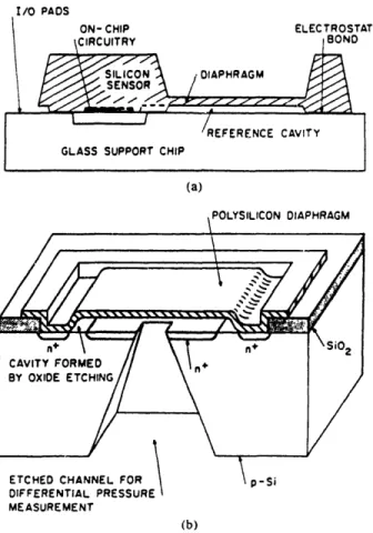
Figure 2.1: Piezoresistive silicon pressure diaphragms (from [3])
average stress), diaphragm size and thickness. All of these factors contribute to a potential decrease in sensitivity and a larger error in the measurement.
This technique is popular as a read-out scheme applied to silicon pressure sensors in spite of large non-linearity for higher-order piezoresistive coefficients and process dependent effects. Temperature coefficients for zero-pressure offset have been re-ported between 1 and 5 mmHg/°C depending on doping levels [151. Temperature compensation is used to reduce these effects despite increased costs. This may be due to the lack of alternate methods of pressure detection besides the capacitive method, which until recently required extensive circuitry [15].
Shown in Figure 1 (2-1) is a typical piezoresistive configuration applied to a silicon diaphragm. In recent years, several novel structures have incorporated this method for pressure and acceleration detection [161-[20J. There have been few im-provements in the reduction of temperature sensitivity due to the inherent mecha-nisms that cause piezoresistivity. This has led others to explore the use of capacitive readout for sensing pressure.
2.1.2
Capacitive Technique
Capacitive pressure sensors detect pressure by a change in capacitance in a de-formable structure. There are no less than six temperature mechanisms in piezore-sistive sensors, three of which appear in the capacitive sensor: plate deflection temperature sensitivity, packaging stress and gas temperature between capacitor plates. These can be easily reduced and controlled so that capacitive sensors fea-ture low temperafea-ture sensitivity [15j. For a capacitive sensor shown in Figure 2 (2-2), the capacitance between the plates is
C
=i
S- w(xy dxdy (2.2)where Eo is the free-space dieiectric constant, S is the zero-pressure plate separa-tion, and w(x,y) is the deflection response to the applied pressure [3]. Studies have shown that with a diaphragm of the same thickness, the intrinsic unloaded pres-sure sensitivity of the capacitive technique is an order of magnitude greater than the piezoresistive technique [31. However for silicon diaphragms, the zero-pressure capacitance may be quite small (on the order of tenths of a picofarad) which com-plicates the capacitance detection circuitry. For particular readout circuits, para-sitic capacitances cause an error in the measurement. The detection circuitry is of paramount importance to the feasibility of such a scheme.
Because of the increased pressure sensitivity and decreased temperature sensi-tivity, the capacitive sensor has become a viable alternative to the piezoresistive sensor. A popular detection method utilizes an oscillator which drives a capacitive bridge circuit. A change in capacitance relative to a reference capacitance causes an output voltage (depending on the output scheme) or shift in frequency which can be detected by an external circuit [21]-[26]. The main cause of error is the
2.1. FORCE DETECTION METHODS 23
I/O PAOS
(a)
MEASUREMENT
(b)
existence of stray parasitic capacitance. In most of the literature, the sense and reference capacitors are often an order of magnitude larger than the parasitics so that errors due to parasitics are either ignored entirely, or are calculated but usually deemed insignificant [22],[24],[261-[29]. It is unclear what the effect of large para-sitic capacitances (when compared to the sense and reference capacitors) will have on these measurement techniques. Major areas of research involve modeling and fabrication of the silicon diaphragms [2],[301-[321 (for better reproducibility), and the development of capacitance detection methods using oscillator-drive techniques [23],[25],[26],[33]. Recently, the advent of switched-capacitive ideas have led to new and innovative methods of capacitance detection [281,[291,[34]. However, problems appear that are inherent to all switched-capacitive circuits. MOS switch charge injection, clock feedthrough, and circuit noise become a major limiting factor in cir-cuit performance. These problems are not new to the MOS analog circir-cuit designer. Switched-capacitive circuits have been applied to filter design and analog-to-digital converters with great success. A majority of problems have been circumvented or solved using novel circuit methods. Such methods are discussed in the next section.
2.2 Calibration Technique: Historical Origins
As mentioned earlier, the capacitive technique offers substantial gains over the piezoresistive method. Common to most capacitive detection schemes is an oscillator-driven detection circuit. Most information processing is accomplished by a micro-processor so that frequently the analog data from the detection circuitry must be converted externally by a data acquisition system. This system is usually not in-cluded as part of the detection scheme, though it plays a key role in sensor
sys-2.2. CALIBRATION TECHNIQUE: HISTORICAL ORIGINS
tern performance. The calibration technique addresses problems associated with switched-capacitive circuits while being an integral part of a data acquisition sys-tem. Digital and analog data are available as a consequence of the technique so that external data conversion is not necessary. The idea was first utilized in mak-ing capacitor mismatch measurements 351, then later extended to analog-to-digital converters employing binary-weighted capacitor arrays [361. Since its origins lie in and charge-redistribution A/D converters, a brief overview of the relevant topics is given.
As demand increased for precision analog circuits, the switched-capacitive idea emerged in analog-to-digital converter designs 371. For high-precision A/D con-verters, individual trimming and component matching are needed. Though this is still the case for extremely high-precision circuits, designers have developed ideas that avoid this costly procedure through clever circuit design. In 1975, a method was presented that measured capacitive mismatches on an IC [35J. It was developed for measuring capacitive mismatches in binary-weighted capacitor arrays because capacitance measurements were inadequate at that time. These arrays were used in a new charge redistribution A/D conversion method [37],[38].
2.2.1
Charge Redistribution A/D Conversion
In Figure 3 (2-3) is a conceptual example of the operation of a five-bit A/D conver-sion using the charge redistribution technique. The components consist of a binary weighted capacitor array, MOS switches, and a comparator. A/D conversion is achieved in three steps:
J /f;O · -2cv,.
/," Vo,
2 4 8 16 16
VmI a. - V
Figure 2.3: Simulation of 5-bit charge redistribution A/D converter (from [37]) 1. Ground the top node so that V is ground. Set the bottom plates of the
capacitors in the array to the input voltage to be converted.
2. Open the top switch so that the top node floats. Connect the bottom plates of the capacitors to ground. These two steps have stored a charge on the top node that is proportional to the binary-weighted sum of the input voltage. 3. Apply a reference voltage Vrf! to the largest capacitor in the array. The output
of the comparator will be the most significant bit of the A/D conversion. If the bit is zero, then return the bottom plate to ground, else continue to the next largest capacitor (C/2) until all N bits have been determined.
To see how these steps are mathematically equivalent to an A/D conversion, consider the charge stored due to the first step. The charge stored is
Q1 = -i. + + - + - + i +
6
= -2VnC2.2. CALIBRATION TECHNIQUE: HISTORICAL ORIGINS 27
After the top node is isolated, voltages are applied to the bottom plates of the capacitors which will redistribute the charge on the top node. If we apply a voltage Vre/ to the largest capacitor (C), the voltage V. can be found due to charge conser-vation, i.e. Q must be equal to any expression of the charge after the top switch is opened. With Vrei applied to the largest capacitor C, the expression for charge becomes
Q2 = 2V.C - Vref C
Setting Q1 = Q2 and solving for V- yields
C
Vz = -vi. + v,,r C
Notice the extra lc capacitor in the array. This is used so that the total capacitance on the node is 2C and hence the capacitive divider ratio will always be a power of 2. Thus
V, = -Vin +
2
The comparator senses V,.
If V > 0 then Vi <
If V <0 then V,,>
More generally, for testing the ith bit in an N-bit conversion, where the LSB is bo
and the MSB is bN-1, the algorithm is
If V > 0 then Vin < EN-i so set bN i = 1 (2.3)
If V < 0 then V,,n > N-i so set bN-, = 0 (2.4)
where EN-i is given by
N-i Vref
N-i = bN- (2.5)
and in actuality, bN-i is set to one (our initial guess), and the comparator will tell us whether to change it to zero or not. This is the key to the A/D conversion. By applying Vref to different binary-weighted values of C, we can either add or subtract these terms to V. The comparator will tell us which terms to keep and which to discard. This is exactly the process of successive approximation A/D conversion.
For N-bit resolution, N redistributions are necessary. After conversion, all the charge will remain on the capacitors representing terms that are kept while others are discharged. The digital code can either be stored sequentially from the compara-tor or can be obtained by looking at the state of the MOS switches after conversion. There are numerous interesting characteristics of this technique. For example, the initial charge sampled on the top node was dependent only on Vn. This need not be the case. If additional charge is added by applying V,,f to the largest capacitor, then essentially this shifts the value of V. so that A/D conversion can accommodate negative inputs, where negative inputs are represented by 1's complement [37].
Parasitic capacitance sensitivity is minimized since it normally is not time-varying. It contributes a charge term in all the steps and therefore cancels out. The accuracy of this technique depends on the control of capacitive ratios. This led to the consideration of new and accurate methods of measuring capacitive mis-matches since ratio matching determined the resolution.
2.2. CALIBRATION TECHNIQUE: HISTORICAL ORIGINS 29 r_ I I I I I I I I I PW SUPPLI I I I I I
L__
Figure 2.4: Capacitive mismatch system (from [351)
2.2.2 Capacitance Mismatch Measurement in A/D
Con-verters
In 1979, McCreary and Sealer published a paper that demonstrated the use of the charge redistribution technique as applied to capacitive mismatch measurement [35]. Capacitance bridges were initially used to measure the arrays but were inadequate due to large-scale non-linearities of the bridge. An algorithm was developed that allowed calculation of ratio errors. Figure 4 (2-4) shows a typical implementation of the algorithm. In the following discussion, the notation for the capacitors is the
following:
Ck = 2kC, k = Oa,Ob, 1,2,, N - 1 (2.6)
Ck denotes a capacitance that is 2 times larger than the unit capacitance C, and
k will take on values from 0 to N - 1, where N is the number of bits of the A/D
converter that uses this binary array. The unit capacitance C is defined such that the total capacitance is exactly equal to 2NC. Notice that there are two capacitors with a value C: C and Co. For the C9 capacitor, the ratio of C9 to the total
capacitance should be one-half. C is the termination capacitor needed to make the capacitive divider ratio always a power of two. In general, the difference between the capacitor Ck and the rest of the array is
k-I
Ck- E C,
This can be calculated for the kth capacitor in two steps:
1. V node is grounded and a voltage V,,f is applied to Ck while grounding all others.
2. The top node is isolated, and the voltages on the capacitors are switched.
The voltage at the top node is, after step 2,
V=
,
Ck -
.
E]Ci
(2.7)
Vt=otal i=lb
Thus the errors due to capacitive mismatches can be found since both V, and V,,F are known.
This technique was implemented to study capacitor mismatch errors that cause linearity errors in charge redistribution A/D converters. Elimination of charge in-jection sources is crucial in obtaining higher resolution and smaller errors in these
2.2. CALIBRATION TECHNIQUE: HISTORICAL ORIGINS 31
A/D converters. In 1984, Lee extended error-correcting ideas to the above tech-nique in achieving a 15-bit A/D converter [36j. The idea of self-calibration allowed higher resolution by eliminating errors caused by component matching and charge injection. It is a powerful concept, and the next chapter is devoted to understanding it. It can be applied to determine precise mismatches of very small capacitors. This is exactly what is needed in capacitive sensor design.
Chapter 3
Self-Calibration Technique:
Theory
3.1 Application to A/D Converters
Successive approximation A/D converters require precise component matching to achieve high resolution and good linearity. Their performance is limited by errors in ratio matching. Higher performance converters usually employ a hybrid tech-nology in order to achieve good component matching. Usually thin and thick film technologies in conjunction with laser-trimming can achieve the small tolerances needed in 16-bit converters. This is a costly procedure since each converter must be specially trimmed.
The self-calibration technique avoids this process by calibrating out errors in component matching. Errors are stored in memory, then recalled when a correction
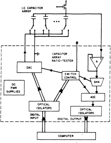
' 1 .. L . . CIi Li !Atb A C , Cs pC, T C,81 Cl1i~T -II (i N c 1- I. DATA OUTPUT COMPA RATOR ;' ,--., tO SUCCESSIVE APPROXIIATtON RE',ITER b '~""lTc r ____ LIBRATON J
-A , E ADDER ATA REGiSTE
l I 1 1 L '
I -- ! '-
I .- __1 i I
.ON * a
Figure 3.1: Block diagram of self-calibrating A/D converter (from [361)
is needed. Calibration can be done at any time, eliminating long-term drift effects. The technique can be implemented in standard CMOS or NMOS technology.
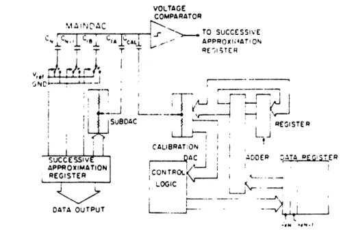
Figure 1 (3-1) shows the block diagram of the self-calibrating A/D converter. It consists of an N-bit capacitor array main DAC (Digital-to-Analog Converter), an M-bit resistor string sub DAC, and a resistor string calibration DAC. The main DAC and the sub DAC are used as the successive approximation A/D converter, while the calibration DAC is used to find and supply the error-correcting voltages to the main DAC. Since the sub and calibration DAC's have errors, two additional bits of resolution are needed to overcome errors in a 16-bit A/D converter [36]. The total resolution for this A/D converter is N + M. The resistor sub DAC is used as the coarse DAC, and the capacitive main DAC is used as the fine-tune DAC. The following discussion focuses on the capacitive main DAC only so that any reference to an A/D conversion refers to the main DAC and not the sub DAC.
3.1. APPLICATION TO A/D CONVERTERS
The calibration cycle computes errors in the mismatch ratio of the capacitor array. In the following discussion, the notation for capacitances is consistent with Section 2.2.3 on capacitive mismatch measurements. It differs somewhat from the original paper by Lee 361. Assume that each binary-weighted capacitor Ck has an error such that
Ck = 2kC(1 + ek), k = Oa,Ob, 1,2, ,N - 1 (3.1)
where C has been defined as an average unit capacitance. In the charge redistribu-tion A/D conversion cycle, the kth capacitor corresponding to the kth bit
determi-nation has a voltage residue on the top node of
V. -V. + Vreif (3.2)
Substituting Ck from equation (3.1) into equation (3.2) yields
V = -V. +
Vref
[ 2C(l + ek) (3.3)The term added to -V,, reduces to
Vr, [ 2C Ek= 2 + ) ] (3.4)
The total sum of errors
ENl
2'Cei is zero since C is defined such that 2NC is thetotal capacitance. Thus equation (3.4) reduces to
re2 - + Vref2- kN Ek (3.5)
The error due to the capacitive mismatch is the last term. Let this be the error voltage
V = Vref2k- N k,
k
= Ob,1, 2, --,
N -1
(3.6) The subscript k refers to the kth capacitor that is 2k times larger than the unit capacitor C. It also refers to the kth bit being determined in the A/D conversion,where N is the number of bits. Total linearity error is
N-I
t%,,o, =
Z
bV(, (3.7)=0Oh
where b, represents the ih bit of the digital output code bN-IbN-2 ..bo. During
the calibration cycle, these errors are measured by a calibration DAC and stored in a RAM. During the conversion cycle, when the ith bit is being determined, the calibration DAC subtracts out the error voltage by applying a voltage to a coupling capacitor connected to the capacitor array.
The self-calibrating technique was developed to reduce the errors due to compo-nent matching in A/D converters. It was used to calibrate out non-linearity errors. Notice that the idea can be equally applied to measuring capacitive differences and
random or controlled sources of charge injection. This technique can measure offset
errors due to capacitive mismatch, comparator offsets and charge injection and can compensate and/or calibrate a system that has these errors. The technique is ideal for measuring capacitive differences (as in capacitive sensors) and reducing inherent circuit errors. The next section describes in detail the application of this idea to the measurement of capacitive differences.
3.2 Application to Measurement of Capacitive
Dif-ferences
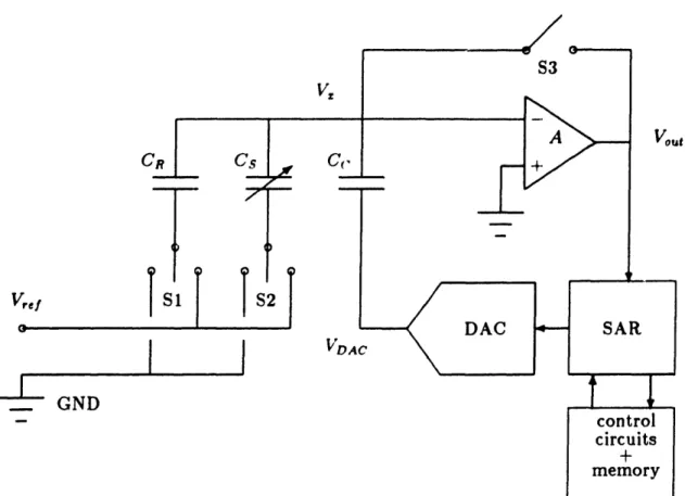
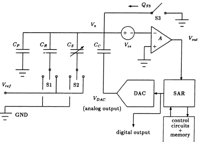
The basic circuit is shown in Figure 2 (3-2). It consists of the sense and reference capacitors (Cs and CR), the coupling capacitor (Cc), three MOS switches, a voltage comparator, a digital-to-analog converter (DAC), a successive approximation regis-ter (SAR), and a memory regisregis-ter with associated logic capable of signal inversion.
3.2. APPLICATION TO MEASUREMENT OF CAPACITIVE DIFFERENCES37
V.
CR
S3
VDAC
Figure 3.2: Ideal AC measurement system
The non-idealities of the circuit appear as the offset of the comparator (Vo,) and its finite gain (A), parasitic capacitance to ground (Cp), and switch charge injection (Qs3). To better understand how these non-idealities are taken into account, the ideal system in Figure 2 is first analyzed, then second-order effects are added later. In the assumption of an ideal circuit, VO, = 0, Cp = 0, Qs3 = 0, A = oo, and DAC quantization error is negligible. The measurement technique proceeds in two steps.
W
it
I
I I
-Step 1
* Set S3 to closed position so that Vz is at ground potential. * Set S to Vref.
* Set S2 to ground. * Set VDAC to ground.
The charge at the top node is just Q1 = -V,feCR. The comparator is implemented with an op-amp so that when the feedback loop is closed with switch S3. V, is at ground potential.
Step 2
* Set S3 to open position. * Set S1 to ground.
* Set S2 to V,,e.
* Initialize SAR/DAC.
When the successive approximation register is initiated, it outputs a voltage that is one-half the full-scale voltage. V responds by either becoming positive or negative relative to ground. The comparator senses this change and output either a one or zero to the SAR. If the output of the comparator is a one, then the SAR keeps that voltage, adds half of the previous voltage, and applies this voltage to Cc. If the output is a zero, then instead of adding half the previous voltage, it subtracts it and
3.3. NON-IDEAL EFFECTS
applies it to Cc. This continues until the SAR reaches its quantization limit and stops. If the SAR, DAC, and voltage comparator are ideal, then the voltage from the DAC (VDAC) precisely forces the top node voltage (V,) to zero. The charge at the top node is thus
Q2 = -V,,fCS - VDACCC
By charge conservation, Ql = Q2 so that
-Vref CR = -V CS - VDACCC
VDAC - Vref(CR - Cs) (3.8)
Cc
The output of the DAC produces a voltage proportional to the capacitive dif-ference of Cs and CR. Appropriate choices of V,,! and Cc can be made so that the maximum dynamic range of the DAC can be utilized. The parameter C can be found by multiplying the numerator and denominator by CR or Cs and rearranging so that
AC _ VDAC
[
CC] (3.9)C
[Vrei] [C
where C is a normalizing capacitance and typically is either CR or Cs. Notice that the result is a product of two ratios: a voltage ratio that can be measured easily, and a capacitive ratio that is equal to the area ratio of the capacitors, given that the dielectric and gap thickness are the same for both capacitors.
3.3 Non-Ideal Effects
In principle, the technique outlined in Section 3.2 should give the difference between two capacitors. However, there are errors introduced when the algorithm is imple-mented in any practical technology. Limitations due to component design, noise,
and physical phenomena cause errors in the measurement. This section deals with these limitations and determines their effect on practical circuit performance of the algorithm.
Possible causes of error in the practical implementation of the algorithm are:
1. Circuit Non-Idealities
(a) MOS switch charge injection (b) Comparator offset with finite gain (c) Parasitic capacitance
(d) SAR/DAC quantization error
2. Component Non-Idealities
(a) Capacitor hysteresis (b) Transistor hysteresis
(c) Junction leakage
(d) Temperature coefficient of the capacitors (e) Voltage coefficient of the capacitors
3. Noise Sources
(a) Switch noise (b) Circuit noise (c) Clock feedthrough
3.3. NON-IDEAL EFFECTS
Item 1 is modeled by a modified ideal circuit block diagram, and the offset calibra-tion algorithm can be applied to eliminate some of these effects. Item 2 represents physical phenomena and their presence is evaluated. Item 3 represents limitations on the practical implementation of the algorithm. Elimination of some but not all of these effects is possible. Finally, Item 4 denotes a random unknown charge generation or recombination factor which could disturb the measurement.
3.3.1 Circuit Non-Idealities
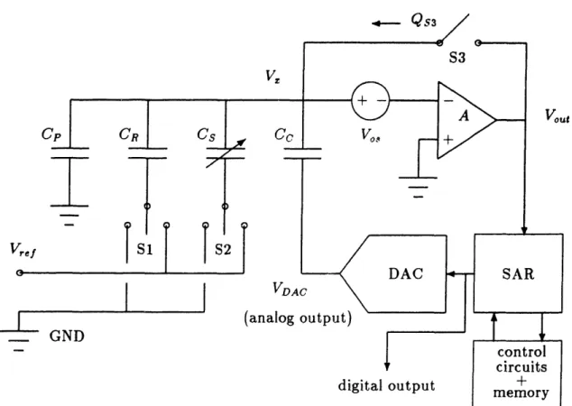
A modified block diagram of the circuit implementation is shown in Figure 3 (3-3). The comparator has an offset V,, and a finite gain A while the switch S3 injects a charge Qs3 when opened. A parasitic capacitance Cp exists as well as a DAC quantization error of ±LSB. It is found that the algorithm can be implemented in either a closed-loop or open-loop topology. In the closed-loop topology, it is important to note that if the feedback path due to switch S3 must cause V = V,, the comparator must operate as an op-amp and cannot be a regenerative latch comparator with only high or low digital outputs. When the SAR/DAC feedback loop is initiated, the operation of the comparator can be limited to digital outputs since the SAR/DAC generate the appropriate analog signal to the coupling capacitor as feedback. Usually the comparator can be designed as a high-gain op-amp that can act as a voltage comparator when its output saturates. In the open-loop topology, the feedback loop through S3 is never used so that the comparator may always have digital outputs. Since the analog signal for measurement of small capacitors is usually small, a monolithic preamplifier can be used to buffer the data to an off-chip comparator in this configuration. In the analysis, the closed-loop is considered first, then the open-loop.
4-- Qs3 Vz T S3 V0 8 VDAC (analog output) digital output
Figure 3.3: Non-Ideal AC measurement system Cp
I
-! C It I-3.3. NON-IDEAL EFFECTS
Closed-Loop Topology
Assuming that VDAC is in error, the amount of error transferred to V. can be easily calculated. Refer to Figure 3 (3-3). A real DAC can typically resolve to i1LSB. Since it has finite resolution, it cannot exactly force Vz to ground. Assuming that Vz is at some voltage V0, and all the capacitors are grounded, the initial charge is
Qi = Vo,(CP + CR + CS + CC)
If VDAC = ±ILSB and the node is isolated, the final charge is
Qf = VZ(Cp + CR + CS) + (V, 1+ LSB)Cc
By charge conservation, Qi = Q so that
Vo,(Cp + CR + CS + CC) = [r2(Cp + CR + CS) + (Vz ± -LSB)Cc
Solving for Vz yields
=
V
,,,
Cp +LSBC +
CS+ CC]=
6(LSB)
(3.10)
where 6 is the capacitive divider ratio
Cc (3.11)
6= CP +CR + CS + CC + + C C Ctotl (3.11)
Thus any change in voltage AV at VDAC results in a change in voltage 6AV at V. This is just a simple capacitive divider as seen from a charge conservation derivation. This introduces an error in the measurement.
Charge injection can be measured using the offset calibration technique. This is called the calibration cycle while the capacitive mismatch measurement is denoted as the measurement cycle. The calibration and measurement cycle inherently eliminate 43
the comparator offset in the closed-loop topology. In the open-loop topology, the offset is measured, then eliminated.
Consider the finite gain of the comparator. In the closed-loop topology, it must behave as a high-gain op-amp in Step 1. The output of the op-amp is
Vout = A(Vo, - Vot)
Vou = [1 A]v
If A is large such that A 1 then Vo,t - V0,. For small input signals, there should
be a preamplifier to buffer the chip to another comparator off-chip. The gain of the preamplifier must be large enough to overcome the hysteresis of the off-chip comparator. This is a small and feasible requirement.
The calibration procedure begins by measuring the charge injection. For gener-ality, assume that the limitation of the DAC may be quantization errors or thermal noise such that the effective resolution of the DAC is ±AV.
Step OA
* Set S3 to closed position. V becomes V,,. * Set S1 to ground.
* Set S2 to V,,I. * Set VDAC to ground.
Assuming that the DAC cannot be a ground but is at ±AV, the charge on the top
node is
3.3. NON-IDEAL EFFECTS
Step OB
* Set S3 to open position. * Initialize SAR/DAC.
The SAR/DAC forces Vx to Vo, ± 6AV. The charge on the top node becomes
QOA + QS3 due to switch injection. After the SAR has finished, the charge can be calculated as
QoB = (V, +
6AV)(C
+ CR + CS + CC) - VrcfCS - VDACCCBy charge conservation, QOA + QS3 = QOB. The offset terms and the VrcfCs terms
cancel. Replacing 6 by equation (3.11) and assuming that in worst case the ±AV terms add, VDAC becomes
-QS3
VDAC,.,, - ± 2ŽAV (3.12)
Cc
Charge injection must be measured since it upsets the charge conservation as-sumption made in the earlier ideal circuit analysis. If it is taken into account, charge due to the capacitors can be accurately determined and hence the capacitive difference. Once the switch injection voltage is measured, it can be stored in a RAM. When the negative of VDAC.,, is applied to the coupling capacitor, a voltage at Vz is created that cancels out the error voltage generated by the switch injection charge. Alternatively, one can think of the DAC as creating a positive charge on the coupling capacitor that is just large enough to cancel the negative switch injection (assuming an NMOS switch) and hence the only charge available for measurement is due to the voltage on the capacitors. The sequence for measurement is
Step 1
* Set S3 to closed position. V becomes V0,.
* Set VDAC to -VDAC,.,,i
* Set S1 to Vrf. * Set S2 to ground.
Assuming that when we apply -VDAC,,,,, it introduces another error tAV, the charge at the top node is
Q1 = Vo,(CP + CR + CS + CC) - VrefCR + VDAC,..,CC ± AVCC
Step 2
* Set S3 to open position. * Set S1 to ground.
* Set S2 to Vrf/.
*
Initialize SAR/DAC. This forces V, = V0, ± 6AV.The charge on the top node becomes Ql + Qs3 due to switch injection. After the SAR finishes, the charge expression can be written as
Q2 = (V,, ± 6AV)(Cp + CR + CS + CC) - VefCS - VDACCC
By charge conservation, Ql + Qs3 = Q2. Replacing VDAC,dI with equation (3.12)
3.3. NON-IDEAL EFFECTS
terms and the offset terms. The ± AV terms do not necessarily cancel and in worst case they add. Solving for VDAC yields
VDACm,, =
V,(CR -
Cs)±
4AV (3.13)In the calibration and measurement sequences, the errors due to the DAC when
-VDAC.., and ground are applied are taken into account. From the calculations
made, one can easily deduce that the DAC is used four times, each time introducing an error of ±AV. Thus the worst case error occurs when all the error terms either add or subtract, ±4AV.
The offset does not effect the technique because it shifts the voltage at Vz to V,, and does not change during the calibration and measurement cycles. Time-varying offsets are considered in a later section.
Effects of parasitic capacitance are canceled. It does impose a constraint on the system. A larger Cp causes a reduction in 6. If 6 becomes too small, Vs becomes pinned by the large Cp and the DAC is not able to adjust V. The ±AV error becomes limited by the capacitive divider ratio and not the quantization error because the minimum amount of control the DAC has is (± 4LSB) which may be less than the comparator resolution. A smaller Cp reduces 6 but increases the kT/C noise so that a trade-off is introduced. This is examined in a later chapter.
Open-Loop Topology
When the measurement technique is done in an open loop configuration as in Fig-ure 4 (3-4), the offset of the comparator is not canceled. This is because the final value of Vz in one step is not the same as the final value of Vz in the other. It
QS3 Vs S3 I VOJ It VDAC (analog output) digital output
Figure 3.4: Non-Ideal AC measurement in open-loop
Cp
I
I llllllll !
1
3.3. NON-IDEAL EFFECTS
can be measured and eliminated in the measurement. In this configuration, the comparator does not need to have analog output capability and can act strictly as a voltage comparator with digital outputs. The calibration sequence is
Step OA
* Set S3 to ground. V is zero, not Vo,. * Set VDAC to ground.
* Set S1 to ground. * Set S2 to V,,/.
The charge on the top plates of the capacitors is
QOA = -VrcICS ± AVCc
Step OB
* Set S3 to open position. * Initialize SAR/DAC.
After the switch S3 is opened, the charge on the top node becomes QOA + Qs3. The
SAR/DAC forces V. to V, ± 6AV since this means a zero voltage at the input of an ideal comparator. The charge at the top node can be written as
QoB = (Vo,
± 6AV)(Cp
+ CR + CS + CC) - Vrf CS - VDACCCBy charge conservation, QOA + Qs3 = QOB. Solving for VDAC,
VDAC
(Vo, ± 6AV)(Cp + CR + CS + CC)
Cc
+ -Qs3
Cc=
CP + CR + CS + cc]
Substituting 6 from equation (3.11) into the above yields, 1 -f ICP
VUAC;I - 's [ + CR + CS +
Cc
CC , -QS3 , A
J Cc
This calibration cycle includes the comparator offset voltage because the top node is not returned to ground but rather to Vo,. The offset can be calibrated out along with the switch injection.
In measurement, the cycle is similar to the closed-loop sequence:
Step 1
* Set S3 to ground. V is zero.
*
Set VDAC = -VDAC,.,.* Set S1 to Vr,,.
* Set S2 to ground.
The charge on the top node is
Q1 = -VrefCR + VDAC,,ICC
± AVCC
VDAC 6
AV [
P +C
R + C+C
cc
-QS3 Cc (3.14) 133. NON-IDEIAL
EFFECTS
Step 2
* Set S3 to open position.
* Set S1 to ground.
* Set S2 to V,tf.
* Initialize DAC/SAR. V2 becomes Vo,, ± 6AV
After the switch S3 opens, the charge on the top node becomes Ql + Qss. After the SAR finishes, the charge on the top node is
Q2 = (Vo,
±
6AV)(Cp + CR + CS + CC) - VreCS - VDACCCBy charge conservation, Ql + Qss = Q2. Substituting equation (3.14) for VDAC,.I,
and noticing that the offset terms and the charge injection terms cancel while the ±AV terms add in worst case, VDAC becomes
VDAC,, Vtef(CR - Cs) ± 4AV (3.15)
Cc
The open-loop measurement yields the same result as the closed-loop. Tile disadl-vantage is that a large comparator offset may yield a calibration voltage larger than the DAC maximum and calibration becomes impossible. The closed-loop is pre-ferred if large variations in offset voltage occur in an IC fabrication process. This is normally the case since offsets are almost impossible to control because of random transistor mismatches.
Summary of Important Equations
For open-loop topology,
VDAC,,i Vo [Cp C R+Cs + CC ] + 'QS ! 2AV
Cc Cc
t VDACma - Vref(CR - CS)
±
4AVCc
For closed-loop topology,
-QS3
VDAC,4 = C + 2AV
VDAC,....
=
Vef (CR - CS)±
4AV CcCapacitive mismatch ratio for both topologies becomes
AC [VDAC, V] CC] (3.16)
where C is either CR or CS. It is the same as equation (3.9) in the ideal circuit case except for the error term,
±[V4]A
[C
(3.17)
This error term determines the minimum resolvable capacitance change. The effect of the parasitic capacitance appears as a constraint on the comparator resolution,
p CRp+CCS + Cc
It should be emphasized that the expression for QS3 is negative since it represents
electrons from the channel of an NMOS switch. A PMOS switch injects holes so
3.3. NON-IDEAL EFFECTS
In the analysis, the charge injection from the switches S1 and S2 is ignored. These switches cannot inject charge onto the top node, and therefore have no effect on V;. For increased switching speed, the on-resistance of the MOSFET channels should be low, requiring the W/L ratios to be large. Consequently, S1 and S2 can be made as large as desired. S3 cannot be made too large since Qs3 is proportional to W/L. Too large a W/L results in QS greater than the DAC range, making calibration impossible. Proper design can balance the tradeoffs involved in choosing the components needed in meeting a specific requirement. These design issues are discussed in Chapter 5.
3.3.2
Component Non-Idealities
In the analysis of Section 3.3.1, the components are treated as ideal elements. A voltage across a capacitor induces a charge on its plates, and when discharged, leaves no residual charge on the plates. Similarly, a MOSFET is assumed to have a constant threshold voltage and thus the comparator offset should not vary with time or input signal. This section discusses the non-ideality of the circuit components and their effect on circuit performance.
Capacitor Hysteresis
Capacitor hysteresis occurs because residual charge remains on a capacitor after it is discharged. Charging the capacitor in the forward direction and returning it to zero results in non-zero charge on the plates. Similarly, charging the capacitor in the reverse direction and returning it to zero yields a non-zero charge which may be different than the forward case. The curve is highly time dependent. If enough
time is allowed, the charge may relax to the zero-charge state. Studies have been made on this phenomena in MOS capacitors, and it appears that it is a function of the voltage applied and the stress time at that voltage [391. Longer times and larger voltages cause the relaxation time of the residual charge to increase. This may be the result of charge-trapping states at typical Si/SiO2 interfaces.
The hysteresis can be measured using the same charge redistribution technique, and has been used to measure the residual polarization in MOS capacitors [391. The analysis is an extension of the analysis in Section 3.2. It is assumed that the capacitors have some residual polarization QR with zero voltage applied in the time frame of interest. Since the calibration cycle does not involve switching and discharging, the charge measured is only the switch injection. During the measurement when Cs is discharged, the charge at the top node due to Cs is not zero, but QR. Similarly, when CR is discharged, the charge at the top node is QR assuming the capacitors share the same process qualities. If we make the analogy that the measurement step for the capacitors is a calibration step involving residual
charges, then the measurement voltage becomes
VDAC,.+
Vf(CR
-Cs)
±
4V +
2QR(3.18)
Cc Cc
where the plus subscript indicates a positive reference measurement (assuming that
CR is greater than Cs). Performing the calibration and measurement cycles again, but with the roles of CR and Cs reversed. VDAC, ... becomes
VDACm, Vref(CS - CR) 4V -2
QR (3.19)
Cc
Cc
where the minus subscript denotes a negative reference measurement. Adding the two equations yields
VDACn..+ + VDAC,n..,- =
![Figure 2.1: Piezoresistive silicon pressure diaphragms (from [3])](https://thumb-eu.123doks.com/thumbv2/123doknet/14746885.578492/21.918.274.712.185.384/figure-piezoresistive-silicon-pressure-diaphragms-from.webp)
![Figure 2.3: Simulation of 5-bit charge redistribution A/D converter (from [37]) 1](https://thumb-eu.123doks.com/thumbv2/123doknet/14746885.578492/26.918.235.676.219.450/figure-simulation-bit-charge-redistribution-d-converter.webp)