HAL Id: hal-01848668
https://hal.archives-ouvertes.fr/hal-01848668
Submitted on 4 Jun 2019HAL is a multi-disciplinary open access archive for the deposit and dissemination of sci-entific research documents, whether they are pub-lished or not. The documents may come from teaching and research institutions in France or abroad, or from public or private research centers.
L’archive ouverte pluridisciplinaire HAL, est destinée au dépôt et à la diffusion de documents scientifiques de niveau recherche, publiés ou non, émanant des établissements d’enseignement et de recherche français ou étrangers, des laboratoires publics ou privés.
Copyright
Huge gain in pyroelectric energy conversion through
epitaxy for integrated self-powered nanodevices
Rahma Moalla, Bertrand Vilquin, Guillaume Saint-Girons, Gwenaël Le Rhun,
Emmanuel Defay, Gaël Sebald, Nicolas Baboux, Romain Bachelet
To cite this version:
Rahma Moalla, Bertrand Vilquin, Guillaume Saint-Girons, Gwenaël Le Rhun, Emmanuel Defay, et al.. Huge gain in pyroelectric energy conversion through epitaxy for integrated self-powered nanodevices. Nano Energy, Elsevier, 2017, 41, pp.43 - 48. �10.1016/j.nanoen.2017.09.001�. �hal-01848668�
Huge gain in pyroelectric energy conversion through epitaxy for
integrated self-powered nanodevices
Rahma Moallaa, Bertrand Vilquina, Guillaume Saint-Gironsa, Gwenael Le Rhunb, Emmanuel
Defayc, Gael Sebaldd,e, Nicolas Babouxf and Romain Bacheleta,*
a
Institut des Nanotechnologies de Lyon, INL-CNRS UMR 5270, Univ. Lyon, Ecole Centrale de Lyon, Bâtiment F7, 36 av. Guy de Collongue, 69134 Ecully Cedex, France
b
CEA, LETI, MINATEC Campus, 17 Rue des Martyrs, 38054 Grenoble, France
c
Luxembourg Institute of Science and Technology (LIST), Materials Research & Technology Department (MRT), 41 Rue du Brill, L-4422 Belvaux, Luxembourg
d
Univ. Lyon, INSA-Lyon, Laboratoire de Génie Electrique et Ferroélectricité, LGEF EA682, F-69621 Villeurbanne, France
e
ELyTMaX UMI 3757, CNRS - Université de Lyon - Tohoku University, International Joint Unit, Tohoku University, Room#503, MaSC Building, Katahira 2-1-1, Aoba-Ku, Sendai, 980-8577, Japan
f
Institut des Nanotechnologies de Lyon, INL-CNRS UMR 5270, Univ. Lyon, INSA de Lyon, Bâtiment Blaise Pascal, 7 avenue Jean Capelle, 69621 Villeurbanne Cedex, France
* Corresponding author.
Graphical abstract 0 5 10 15 1E-4 1E-3 0.01 0.1 1 10 W D (m J/c m 3 ) T (°C) Epitaxial Polycrystalline Epi vs Poly Si(001) Si(001) TiO2 Pt PZT STO SRO PZT Research highlights
Epitaxial PZT layer yields pyroelectric energy conversion with two orders of magnitude larger than its polycrystalline counterpart.
Pyroelectric extrinsic contribution is discriminated through static and dynamic measurements.
Extrinsic pyroelectric contribution due to domain wall motion appears detrimental for properties and is almost twice larger with polycrystalline layer than with epitaxial layer.
Around 1 mJ/cm3 per cycle with 6 K temperature variations can be reached with epitaxial layers, which is enough to efficiently power autonomous nanodevices.
ABSTRACT
Polycrystalline (textured) and epitaxial 500 nm thick Pb(Zr0.52Ti0.48)O3 (PZT) layers have
been monolithically integrated in metal-insulator-metal structure on silicon in order to compare their pyroelectric properties, both statically (under stabilized temperatures) and dynamically (when submitted to temperature transient as a pyroelectric device should work). The films have roughly the same out-of-plane orientation, and thus a similar out-of-plane remnant ferroelectric polarization around 12 C/cm2. Whereas their static pyroelectric coefficients are similar (around -470 C m-2 K-1), the dynamic pyroelectric coefficient of the epitaxial layer is about one order of magnitude larger than that of the polycrystalline layer (-230 vs -30 C m-2 K-1). This causes an important difference on the densities of converted pyroelectric energy by almost two orders of magnitude (1 vs 1.5 10-2 mJ/cm3 per cycle for
temperature variations of 6 K). This difference is explained here by the counterbalanced extrinsic pyroelectric contribution arising from the domain walls motion in the dynamical measurements. Extrinsic pyroelectric contribution appears almost twice larger on polycrystalline layer than on epitaxial layer (+430 vs +250 C m-2 K-1). These results are crucial for further design of advanced integrated pyroelectric-based nanodevices.
1. Introduction
The development of competitive devices in the microelectronic industry is essentially driven by advanced materials integration on semiconductor wafers (mainly Si) for new functionalities, low-cost processing and device reliability/efficiency. Perovskite oxides are very appealing materials since they can exhibit an incredible range of remarkable robust properties (such as ferroelectricity, piezoelectricity, pyroelectricity, ferromagnetism) and since they can be monolithically integrated on Si to address a wide range of applications (memories, sensors, actuators, harvesters,...) [1-4]. It is generally admitted that functional oxides, in particular ferroelectric oxides, have to be integrated in epitaxial layers because of their crystallographic orientation dependent functional properties. In particular, extrinsic effects due to domain walls (DWs) motion may moderate the functional properties. These effects are expected to be larger in polycrystalline layers, having larger density of DWs, than in epitaxial layers. However, this general assessment has not been clearly addressed experimentally, and in some cases polycrystalline layers have been found to be as efficient as epitaxial layers [5]. Comparative studies between polycrystalline layers and epitaxial layers are very rare, and the impact of epitaxy on the functional properties of oxide layers properties remains confused, whereas the integration of epitaxial oxide layers on silicon represents a significant technological complexity [4,6-9].
Pyroelectric (PE) oxides are very appealing for a broad range of devices (sensors, harvesters, transducers,...) because their thermal, optical and electrical responses are intimately coupled
[10-16]. For instance, thanks to a large pyroelectric coefficient (p) [12], reference Pb(ZrxTi
1-x)O3 (PZT) films have been used as thermal energy harvester to power wireless sensors [14].
In addition, because of its large piezoelectric coefficient and photovoltaic effects, PZT films have recently been used in single structures to harvest simultaneously mechanical, thermal and solar energies [17]. Also, flexible pyroelectric nanogenerators have been realized using a composite structure of KNbO3 nanowires [18]. Pyroelectric devices work dynamically with
external stimuli fluctuations (for instance temperature or light) [10-16]. In a pyroelectric material, the total PE coefficient is the sum of the primary coefficient (composed of intrinsic and extrinsic coefficients at constant strain) and secondary coefficient (the piezoelectric contribution from thermal expansion) [10,19,20]. The intrinsic (native) contribution to the pyroelectric effect arises from polarization variation of ferroelectric domains due to a temperature change, whereas the extrinsic contribution arises from DWs motion due to temperature variation. Similar to the case of dielectric, ferroelectric and piezoelectric properties [5,21-23], extrinsic contributions arising from DWs motions can negatively impact the pyroelectric and electrocaloric properties of PZT films [11,19-20,24]. Extrinsic PE contribution exists in polydomain c/a/c/a epitaxial PZT films with 90° DWs [20]. It is predicted to be particularly large with mainly c-domains orientation and negligible with mainly a-domains orientation. However, comparison between extrinsic PE contributions in polydomain epitaxial films compared to their polycrystalline counterparts has not been reported yet.
Here, polycrystalline (textured) PZT film and epitaxial PZT film, monolithically integrated on Si, are compared. By measuring PE coefficient statically (without extrinsic contribution) and dynamically (with extrinsic contribution), we demonstrate a large detrimental extrinsic PE contribution in polycrystalline PZT films with respect to epitaxial PZT films by about a factor two, that gives a difference of almost one and two orders of magnitude on the effective total PE coefficients and on the converted PE energy densities, respectively. These results are of critical importance in the design of integrated PE devices of advanced properties.
2. Experimental section
Five hundred nanometers thick PbZr0.52Ti0.48O3 (PZT) layers were grown by using the same
sol-gel process for both heterostructures, starting from a commercial solution with lead excess (PZT 110/52/48, provided by Mitsubishi Materials Corporation) to compensate lead volatility
during the subsequent crystallization annealing under oxygen flux at 650°C. One spin-coating step yields 33 nm thick PZT layer, so that 15 spin-coating cycles have been applied here to both samples to obtain 500 nm thick PZT films. Details on the sol-gel process for the deposition of PZT layers can be found elsewhere [9,25]. The thickness of the films has been monitored and calibrated by X-ray reflectometry (up to 100 nm thick films), scanning electron microscopy and transmission electron microscopy in cross sections (up to micrometer thick films).
Film A (epitaxial) has been deposited on a 30 nm thick SrRuO3 (SRO) layers epitaxially
grown by radio frequency magnetron sputtering at 800 °C under 5 × 10⁻³ mbar of partial
oxygen pressure on (001)-oriented single-crystalline Si substrate buffered with 10 nm thick epitaxial STO layers grown by oxide molecular beam epitaxy (MBE) [8,9,26,27]. The SRO layer is used as lattice-matched bottom electrode in the built-in metal–insulator–metal (MIM) capacitor epitaxial heterostructure. Film B (polycrystalline) has been deposited on polycrystalline Pt-coated silicon substrate. Ten nm thick Ti layer and 100 nm thick Pt layer are subsequently deposited on Si(001) by magnetron sputtering. Ti is used as an adhesive layer for the Pt layer which is used as a bottom electrode. The subsequent annealing steps lead to the oxidation of Ti layer and Si interface.
A high-brilliance Rigaku SmartLab X-ray diffractometer (XRD) equipped with a 9 kW rotating anode and a two-bounce Ge(220) monochromator was used to investigate the structural properties of the layers (crystalline orientation, cell parameters and mosaicity). After the PZT growth, Pt was deposited by sputtering at room temperature on top of the samples and square-shaped top electrodes were fabricated using a UV-lithography and lift-off process for further macroscopic electrical characterization in bottom-top configuration. The static pyroelectric properties were determined by measuring ferroelectric hysteresis loops (polarization versus electric field) at different stabilized temperatures from 300 K to 400 K, in bottom-top configuration and using the PUND method with triangular shape pulses of 1 ms
rising time [9]. The dynamic pyroelectric properties were estimated by measuring in bottom-top configuration the PE current induced by applied temperature variations also from 300 K to 400 K without electric field at heating rates up to 2 K/s.
3. Results and discussion
For clarity, the epitaxial heterostructure (PZT/SRO/STO/Si) is labeled sample A and the polycrystalline heterostructure (PZT/Pt/TiO2/Si) is labeled sample B (see experimental section
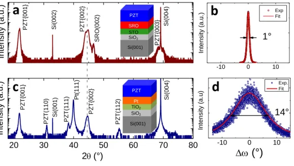
for fabrication details). The XRD measurements recorded on both heterostructures are displayed in Figure 1. The /2 scans provide information on the out-of-plane orientations and lattice parameter of the PZT layers (Fig. 1a,c) whereas the widhts of the -scans are a measure of their mosaicity (Fig. 1b,d). For sample A (PZT on epitaxial STO-buffered Si), the /2 scan only presents {00l}-reflections (Fig. 1a), showing that the PZT layer is fully {00l}-oriented. In this case, the mosaicity of the PZT layer is relatively low, around 1° (Fig. 1b), as expected with epitaxial PZT layers on Si [9]. By contrast, on sample B (PZT on polycrystalline Pt-coated Si), the /2 scan contain all allowed PZT reflections ((100), (110), (111), (112)), which is the signature of a polycrystalline film (Fig. 1c). However, despite lower factor structures as compared to that of the (110) reflection [28], the (00l) reflections dominate the diffractogram recorded on sample B, indicating that the film B is textured with a preferential {00l} out-of-plane orientation. From relative intensity and taking account the structure factors, {00l} texturation is estimated to be around 99%. The mosaicity of the {00l}-oriented domains, measured on {002} PZT Bragg peak, is however very large (width of the -scan of about 14°), as expected from a textured film (Fig. 1d). It is worth noting that the out-of-plane lattice parameters of the {00l} domains are similar in both cases of about 4.05 Å, suggesting the composition of the PZT layer is made of mixed a- and c-oriented PZT {00l} domains, as previously observed for films grown using similar procedures [9]. The relative
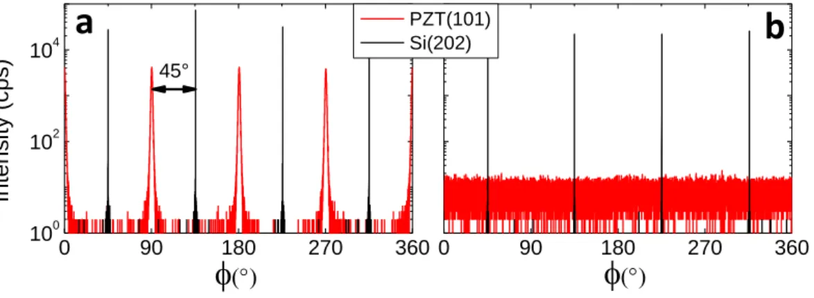
proportions of c-oriented domains are estimated to be close to 44% and 37% for sample A and B, respectively, as deduced from deconvolutions of the PZT {002} peaks (not shown here). Preferential in-plane orientation has been investigated by -scan measurements on asymmetric PZT (101) reflections of the {001}-oriented domains (Figure 2). In sample A, 90°-periodic PZT peaks appeared, spaced by 45° from Si (202) reflections (Fig. 2a). This result confirms that the PZT layer is epitaxial in this case with single in-plane orientation rotated by 45° from the Si lattice. The epitaxial relationship can be written as follows: [100]PZT(001)//[100]SRO(001)//[100]STO(001)//[110]Si(001), as previously reported [9]. In the other case (sample B), no peak has been observed within the 360° -range (Fig. 2b), meaning that, in this case, the predominant {001}-oriented PZT crystals are totally randomly-oriented in-plane.
Ferroelectric and static PE properties of both samples have been measured by recording ferroelectric hysteresis loops (Polarization against electric field E) from room temperature to 400 K (Figure 3). At room temperature, the remnant polarizations (Pr) are roughly similar for
both samples, according to the similar out-of-plane structural properties. Pr is slightly larger
for the epitaxial film A (12.5 C/cm2, Fig. 3a) than for the textured film B (11.5 C/cm2, Fig. 3b), certainly because of the somewhat larger ratio of c-oriented domains in sample A. When the temperature increases, Pr decreases linearly as expected since the measurements are done
well below the Curie temperature. The temperature dependence of Pr is plotted in Fig. 3c for
both samples. The linear slope (Pr/T) gives the "static" pyroelectric coefficient (pstat) which does not contain the extrinsic contribution. The measured pstat are similar for both samples, although slightly higher for epitaxial heterostructure: -480 and -460 C m-2 K-1 for samples A and B, respectively. These values are significantly larger than those reported by other groups with dynamic measurements [12,20,29]. This difference is explained by the fact that the extrinsic contribution, contained in the dynamic measurements, is of opposite sign
(positive) as pointed out theoretically by Karthik et al. [19] and hence diminishes the total absolute value of p.
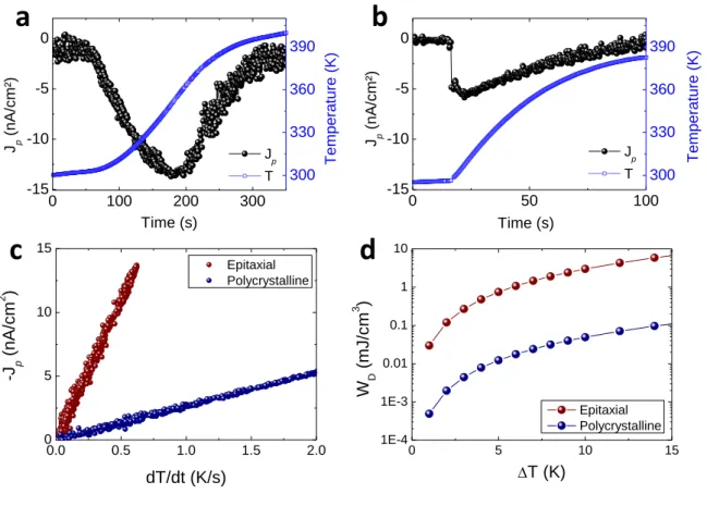
Dynamic PE properties (containing all the contributions) were measured in the same temperature range (from room temperature to 400 K) and in the same bottom-top configuration (Figure 4). To do so, a non-linear upward temperature ramp was imposed to the samples without applied electric field while measuring the PE current (ip):
ip = pdyn S dT/dt = dQ/dt , (1)
where pdyn is the total PE coefficient measured in dynamic mode, S the contact surface area, dT/dt the rate of temperature variation, and dQ/dt the rate of surface charge variation [12]. For sample A, a maximum PE current density (Jp = ip / A) of 13.5 nA/cm2 is obtained at a heating
rate of 0.6 K/s (Fig. 4a). By contrast for sample B, a maximum of 5.2 nA/cm2 only is obtained for a much larger heating rate of 2 K/s (Fig. 4b). The measured PE current densities (Jp) are plotted for both samples as a function of the heating rate (dT/dt) in Fig. 4c. The slopes correspond to the PE coefficients (pdyn) including all the contributions. The pdyn values recorded from these measurements are -230 and -29.5 C m-2 K-1 for sample A and B, respectively. The pdyn value for sample A is in agreement with values reported by another group with epitaxial PZT films [20,29]. For sample B, pdyn is about one order of magnitude lower than sample A, showing, as both samples present comparable static PE properties, that the extrinsic effect is much more important for the polycrystalline layer. We attribute this to a larger ratio of domain walls in the polycrystalline layer. The respective extrinsic contributions (pext = pdyn - pstat) are thus deduced to be +250 and +430.5 C m-2 K-1 for sample A and B, respectively. A non negligible extrinsic contribution occurred also on sample A, about half of that measured for sample B. This contribution comes from the motion of domain walls at the mixed c/a domains in the epitaxial layer, in very good agreement with theoretical results [19]. The theoretical results by Karthik et al. in epitaxial PZT polydomain layers have shown extrinsic contribution up to + 230 C m-2 K-1 for 50/50 PZT composition [19], in very good
agreement with our experimental results (+ 250 C m-2 K-1 in our epitaxial case with 52/48 PZT composition). However, the extrinsic PE coefficient (pext) in polycrystalline layer is of the same order (with opposite sign) as that measured statically (pstat without extrinsic contribution) that makes the total PE coefficient (pdyn) decreasing almost to zero.
This difference between the samples is even larger when estimating the density of PE energy conversion (WD) because it involves the square of the PE coefficient in dynamic mode
[11,12,30]. Based on these dynamical measurements, WD is estimated by a synchronized
electric charge extraction technique using the following equation [30]:
WD = pdyn2T2 / 33 , (2)
where ε33 is the dielectric constant along the out-of-plane direction and ΔT is the temperature
change. ε33 is similar for both samples, and since the harvesting cycles are done under electric
field in the linear regime, 33r = 200 at E = 600 kV/cm has been taken for the estimation of
energy conversion (See 33r against electric field E in Figure S1). The converted pyroelectric
energy densities are plotted as a function of the temperature change in Fig. 4d. They are almost about two orders of magnitude larger for epitaxial layer than polycrystalline layer. For instance with 6 K temperature variations, 1 mJ/cm3 per cycle is reached with epitaxial layer, whereas only 1.5 10-2 mJ/cm3 per cycle is obtained with polycrystalline layer. The energy
harvested by the epitaxial layer would be sufficient to power autonomous sensors for internet of things (IoT) and wireless sensor networks (WSNs) for instance [12,14,30]. The present study conducted on PZT layer here as a reference can be straightforwardly extended to other pyroelectric materials deposited in thin film form.
4. Conclusions
In summary, lead zirconate titanate (PZT) layers were monolithically integrated on Si with polycrystalline and epitaxial quality in metal–insulator–metal (MIM) structure. Pyroelectric (PE) coefficients (p) were determined through static and dynamic measurements in order to
deduce the extrinsic PE contribution. In polycrystalline layer, extrinsic PE contribution is found to be of opposite sign and roughly as high as that measured statically (without extrinsic contribution), making the effective p measured dynamically (all contributions) very low of about one order of magnitude lower than that in epitaxial layer. This important p difference yields a huge difference of two orders of magnitude in terms of converted PE energy density. These results are of critical importance for the design of integrated PE devices on Si.
Acknowledgements
The European commission, the national French research agency (ANR), the French government and STMicroelectronics (S. Monfray, Crolles) are gratefully acknowledged for financial supports through the projects SITOGA (FP7-ICT-2013-11-619456), TIPS (H2020-ICT-02-2014-1-644453), ANR HIRIS, ANR DIAMWAFEL, and Nano2017. The authors also acknowledge the region Rhône-Alpes for the doctoral fellowship of R. Moalla, the “Cellule Energie” of the Centre National de la Recherche Scientifique (CNRS-INSIS) for the financial support of the exploratory project PEPS “PYROS”, and the Ecole Centrale de Lyon (ECL) for the funding of emergent thematic and transversal projects. E.D. acknowledges the Luxembourg National Research Fund (FNR) that helped in financing this research through the COFERMAT project (FNR/P12/4853155/Kreisel). Finally, INL authors acknowledge P. Regreny, C. Botella, and J.-B. Goure for technical assistance on the Nanolyon technological platform.
Appendix A
Supplementary data associated with this article can be found in the online version at
References
[1] S. B. Ogale (Ed.), Thin films and heterostructures for oxide electronics, New York (NY): Springer; 2005.
[2] E. Defaÿ (Ed.), Ferroelectric dielectrics integrated on silicon, Wiley-ISTE, 2013. [3] E. Defaÿ (Ed.), Integration of ferroelectric and piezoelectric thin films: concepts and
applications for microsystems, Wiley-ISTE, 2011.
[4] A. Demkov, A. B. Posadas, Integration of functional oxides with semiconductors, New York (NY): Springer, 2014.
[5] V. G. Koukhar, N. A. Pertsev, R. Waser, Phys. Rev. B 64 (2001) 214103.
[6] J. W. Reiner, A. M. Kolpak, Y. Segal, K. F. Garrity, S. Ismail-Beigi, C. H. Ahn, F. J. Walker, Adv. Mater. 22 (2010) 2919.
[7] S.-H. Baek, C.-B. Eom, Acta Mater. 61 (2013) 2734.
[8] G. Saint-Girons, R. Bachelet, R. Moalla, B. Meunier, L. Louahadj, B. Canut, A. Carretero-Genevrier, J. Gazquez, P. Regreny, C. Botella, J. Penuelas, M. G. Silly, F. Sirotti, G. Grenet, Chem Mater. 28 (2016) 5347.
[9] R. Moalla, B. Vilquin, G. Saint-Girons, G. Sebald, N. Baboux, R. Bachelet, CrystEngComm 18 (2016) 1887.
[10] S. B. Lang, Phys. Today 58 (2005) 31.
[11] S. P. Alpay, J. Mantese, S. Trolier Mc-Kinstry, Q. Zhang and R. W. Whatmore, MRS Bull. 39 (2014) 1099.
[12] C. R. Bowen, J. Taylor, E. LeBoulbar, D. Zabek, A. Chauhan and R. Vaish, Energy Environ. Sci. 7 (2014) 3836.
[13] Y. Yang, W. Guo, K. C. Pradel, G. Zhu, Y. Zhou, Y. Zhang, Y. Hu, L. Lin, Z. L. Wang, Nano Letters 12 (2012) 2833.
[14] Y. Yang, S. Wang, Y. Zhang, Z. L. Wang, Nano Letters 12 (2012) 6408.
[16] G. Sebald, D. Guyomar, A. Agbossou, Smart Mater. Struct. 18 (2009) 125006. [17] K. Zhang, S. Wang, Y. Yang, Adv. En. Mater. 7 (2017) 1601852.
[18] Y. Yang, J. H. Jung, B. K. Yun, F. Zhang, K. C. Pradel, W. Guo, Z. L. Wang, Adv. Mater. 24 (2012) 5357.
[19] J. Karthik and L. W. Martin, Phys. Rev. B 84 (2011) 024102.
[20] J. Karthik, J. C. Agar, A. R. Damodaran and L. W. Martin, Phys. Rev. Lett. 109 (2012) 257602.
[21] F. Xu, S. Trolier-McKinstry, W. Ren, B. Xu, Z.-L. Xie, K. J. Hemker, J. Appl. Phys. 89 (2001) 1336.
[22] N. Setter, D. Damjanovic, L. Eng, G. Fox, S. Gevorgian, S. Hong, A. Kingon, H. Kohlstedt, N. Y. Park, G. B. Stephenson, I. Stolitchnov, A. K. Taganstev, D. V. Taylor, T. Yamada, S. Streiffer, J. Appl. Phys. 100 (2006) 051606.
[23] R. A. Wolf and S. Trolier-McKinstry, J. Appl. Phys. 95 (2004) 1397. [24] J. Karthik, L. W. Martin, Appl. Phys. Lett. 99 (2011) 032904.
[25] R. Moalla, G. Le Rhun, E. Defay, N. Baboux, G. Sebald, R. Bachelet, Thin Sol. Films 601 (2016) 80.
[26] G. Delahaye, C. Merckling, M. El-Kazzi, G. Saint-Girons, M. Gendry, Y. Robach, G. Hollinger, J. Appl. Phys. 100 (2006) 124109.
[27] G. Niu, G. Saint-Girons, B. Vilquin, G. Delhaye, J.-L. Maurice, C. Botella, Y. Robach, G. Hollinger, Appl. Phys. Lett. 95 (2009) 062902.
[28] See the JCPDS sheet number 00-033-0784.
[29] R. V. K. Mangalam, J. C. Agar, A. R. Damodaran, J. Karthik, L. W. Martin, ACS Appl. Mater. Interfaces 5 (2013) 13235.
[30] G. Sebald, E. Lefeuvre, D. Guyomar, IEEE Trans. Ultrason. Ferroelectr. Freq. Control 55 (2008) 538.
Figures and captions 20 30 40 50 60 70 80 Si (0 0 4 ) PZ T (1 1 2 ) PZ T (1 1 1 ) Pt(1 1 1 ) PZ T (1 1 0 ) Si (0 0 1 ) SR O (0 0 2 ) Si (0 0 2 ) Si (0 0 4 ) PZ T {00 1 } PZ T {00 2 } PZ T {00 1 } PZ T {00 3 } 2(°) Int ens it y (a. u. ) PZ T {00 2 } Int ens it y (a. u. ) Si(001) SiO2 STO SRO PZT Si(001) SiO2 TiO2 Pt PZT -10 0 10 Int ensit y (a.u)
(°)
Exp. Fit 14° -10 0 10 Exp Fit Int ensit y (a.u. ) 1°a
b
c
d
Figure 1. XRD /2 scans (a,c) and -scans around the {002} reflection (b,d) of PZT film deposited on (a,b) on SRO/STO/Si (sample A) and (c,d) on Pt/TiO2/Si (sample B).
0 90 180 270 360 0 90 180 270 360 100 102 104
I n te n si ty (cp s) PZT(101) Si(202)
45°a
b
Figure 2. XRD -scans in the Bragg position of the asymmetrical {h0h} reflections of the {00l}-oriented PZT domains (a) on SRO/STO/Si (sample A) and (b) on Pt/TiO2/Si (Sample
300 350 400 6 9 12 Pr ( C /c m 2 ) Temperature (K) PZT/SRO/STO/Si PZT/Pt/Ti/Si Linear fit Linear fit -800 -400 0 400 800 -15 -10 -5 0 5 10 15 300 K 315 K 335 K 355 K 375 K 395 K P (µC /c m ²) E(kv/cm) -800 -400 0 400 800 -15 -10 -5 0 5 10 15 300 K 325 K 350 K 375 K 400 K E(kV/cm) P (µC /c m ²)
a
b
c
Figure 3. Ferroelectric hysteresis loops of polarization measured in bottom-top configuration
and PUND method from room temperature to 400 K of PZT film deposited on (a) SRO/STO/Si (sample A) and (b) Pt/TiO2/Si (sample B). (c) Corresponding temperature
0.0 0.5 1.0 1.5 2.0 0 5 10 15 -J p ( nA/c m 2 ) dT/dt (K/s) Epitaxial Polycrystalline 0 100 200 300 -15 -10 -5 0 Jp T Time (s) J p ( nA/c m ²) 300 330 360 390 T emperat ure (K) 0 50 100 -15 -10 -5 0 T emperat ure (K) Jp T J p ( nA/c m ²) Time (s) 300 330 360 390
a
b
c
d
0 5 10 15 1E-4 1E-3 0.01 0.1 1 10 W D ( m J /c m 3 ) T (K) Epitaxial PolycrystallineFigure 4. (a-b) Pyroelectric current density (Jp) measured in bottom-top configuration at zero electric field under temperature variations from room temperature to 400 K, of PZT film deposited on (a) SRO/STO/Si (sample A) and (b) Pt/TiO2/Si (sample B). (c) Jp plotted in
function of the heating rate (dT/dt). (d) Density of the pyroelectric energy conversion in function of the temperature variations under 600 kV/cm for both heterostructures.