HAL Id: hal-02539609
https://hal.archives-ouvertes.fr/hal-02539609
Submitted on 10 Apr 2020
HAL is a multi-disciplinary open access
archive for the deposit and dissemination of
sci-entific research documents, whether they are
pub-lished or not. The documents may come from
teaching and research institutions in France or
abroad, or from public or private research centers.
L’archive ouverte pluridisciplinaire HAL, est
destinée au dépôt et à la diffusion de documents
scientifiques de niveau recherche, publiés ou non,
émanant des établissements d’enseignement et de
recherche français ou étrangers, des laboratoires
publics ou privés.
Pin Photodetectors for Energy-Efficient Silicon
Interconnects
Daniel Benedikovic, Léopold Virot, Guy Aubin, Jean Michel Hartmann, Farah
Amar, Bertrand Szelag, Xavier Leroux, Carlos Alonso-Ramos, Paul Crozat,
Eric Cassan, et al.
To cite this version:
Daniel Benedikovic, Léopold Virot, Guy Aubin, Jean Michel Hartmann, Farah Amar, et al..
Com-prehensive Study on Chip-Integrated Germanium Pin Photodetectors for Energy-Efficient Silicon
In-terconnects. IEEE Journal of Quantum Electronics, Institute of Electrical and Electronics Engineers,
2020, JQE Special Virtual Issue Dedicated to the 21st European Conference on Integrated Optics
(ECIO), 56 (1), �10.1109/JQE.2019.2954355�. �hal-02539609�
Abstract—Optical interconnects are promising alternatives to
copper-based wirings in on-chip communications. Recent advances in integrated group-IV nanophotonics should address a range of challenges related with speed, energy consumption and cost. Monolithically integrated germanium pin photodetectors on silicon-on-insulator (SOI) waveguides are indispensable devices in this buoyant research field. Here, we comprehensively investigate the opto-electrical properties of hetero-structured pin photodetectors. All photodetectors were fabricated on top of 200-mm SOI substrates using industrial-scale semiconductor manufacturing processes. Under a low-bias voltage supply of 1 V, pin photodetectors exhibit dark-currents from 5 nA to 100 nA, dark current densities from 0.404 A/cm2 to 0.808 A/cm2,
responsivities in a range of 0.17 A/W to 1.16 A/W, and cut-off frequencies from 7 GHz to 35 GHz, respectively. Such achievements make them promising for use in power-efficient optical links operating at 40 Gbps, with a device energy dissipation of only few fJ per bit.
Index Terms—Complementary metal-oxide-semiconductor technology, germanium photodetectors, inter- and intra-chip interconnects, optical communications, silicon nanophotonics.
I. INTRODUCTION
PTICAL interconnects has superseded electrical wirings for inter and intra-chip links due to the performance limits of the latter. Driven by the exponential growth in Internet traffic and portable digital communications, optical solutions are looking increasingly promising not only for long-haul fiber systems, but also in emerging industries such as short-reach data centers, clouds or high-performance
Manuscript received June4, 2019. This work was supported by the European Union’s Horizon 2020 research and innovation program (ERC POPSTAR – grant agreement no. 647342).
D. Benedikovic, G. Aubin, F. Amar, X. Le Roux, C. Alonso-Ramos, P. Crozat, É. Cassan, D. Marris-Morini, and L. Vivien are with the Centre de Nanosciences et de Nanotechnologies, CNRS, Université of Paris Sud, Université Paris-Saclay, 91120 Palaiseau, France (corresponding author: phone: +33 01 70 27 02 98; e-mail: daniel.benedikovic@c2n.upsaclay.fr).
L. Virot, J.-M. Hartmann, B. Szelag, J.-M. Fédéli, and C. Kopp are with the University Grenoble Alpes and CEA, LETI, Minatec Campus, F-38054 Grenoble, Grenoble Cedex, France (e-mail: leopold.virot@cea.fr).
C. Baudot and F. Boeuf are with the Technology R&D, STMicroelectronics SAS, 850 rue Jean Monet, 38920 Crolles, France (e-mail: frederic.boeuf@st.com).
computing, amongst other. Therefore, optical interconnects at the chip-scale level are presently used to address a range of challenges associated with affordable speed, energy consumption and cost [1-6].
Recent advances in nanophotonics yielded compact and high-performance devices on a single chip [5, 6]. Nanophotonics is notably based on a class of materials known as group-IV elemental semiconductors such as silicon (Si) and germanium (Ge) [7-12].
Si, an indirect bandgap material with an energy of 1.1 eV, is an excellent material for low-loss waveguides and high-performing passive devices at near-and mid-infrared (near- and mid-IR) wavelengths [1, 9-11]. In contrast, Ge with its direct bandgap energy of 0.8 eV only, provides several distinctive advantages and complementarities over Si chips and addresses major Si limitations [1]. Optical absorption is indeed high in Ge over the 1.3 – 1.55 µm wavelength range used for fiber-optic communications. The epitaxy of Ge over Si has otherwise progressed tremendously over the last twenty years. Finally, mature process steps using complementary metal-oxide-semiconductor (CMOS) tools and procedures are nowadays available to process Ge-based devices [11, 12]. Intensive efforts are underway to use Ge and/or Ge-based alloys for light emission [13], modulation [14, 15], and detection [16]. In this active research field, the synergy between mature semiconductor manufacturing infrastructure, high fabrication yield, and low fabrication cost is the key for future monolithic integrated circuits [7, 8].
Ge-based photodetectors have been extensively studied since the late 1990s [17-39]. Nowadays, Ge photodetectors have performance metrics, which are close to that of III-V materials. Ge detectors are currently available in open-access platform offerings through foundry sharing initiatives [8], as they are compatible with other passive and active devices on standard silicon-on-insulator (SOI) platforms.
Ge photodetectors integrated at the end of optical waveguides are more appealing for nanophotonics than surface-illuminated devices. In a wave-guided on-chip detection scheme, the optical absorption path is indeed de-coupled from the carrier collection path. In other words, light absorption occurs along the optical mode propagation direction and perpendicularly to the carrier collection path.
Comprehensive study on chip-integrated
germanium pin photodetectors for
energy-efficient silicon interconnects
Daniel Benedikovic, Léopold Virot, Guy Aubin, Jean-Michel Hartmann, Farah Amar, Bertrand
Szelag, Xavier Le Roux, Carlos Alonso-Ramos, Paul Crozat, Éric Cassan, Delphine Marris-Morini,
Charles Baudot, Frédéric Boeuf, Jean-Marc Fédéli, Christophe Kopp, and Laurent Vivien
This approach advantageously circumvents the conventional design trade-off between device responsivity (quantum efficiency) and device speed (opto-electrical bandwidth) and fits modern CMOS processes [1, 16]. Since the first successful implementation of this concept by Ahn, et al., a large number of architectures have been proposed and experimentally demonstrated. Ge homo-junction [17-31] and Si-Ge-Si hetero-junction [32, 35-40] photodetector arrangements have notably been evaluated. Both types of devices consist in pin junction arrangements, with a light absorption occurring in the intrinsic regions. The performances of full-Ge devices are hindered by process issues and optical considerations (i.e. no light confinement in the intrinsic detector region). In homo-junctions photodetectors, ion implantation is used to fabricate heavily n-type and p-type doped side regions, which then have to be contacted to metal via. Both process steps are not as performant in Ge as in Si. This results in slower responses, reduced photo-responsivities, and higher dark-currents in homo-junction structures [17-31]. In contrast, hetero-structured Ge photodetectors with full Si via-contacts and doping scheme avoid Ge processing issues and might substantially simplify the process flow [32, 35-40]. For example, the same masking, ion implantation, and metal contacting steps can be used for the fabrication of active optical link components such as Si modulators and Si-Ge-Si photodetectors [41]. This architecture also leads to the flexible control of the light confinement in the intrinsic region. Such photodetectors have been realized and demonstrated with significantly improved performances in near-IR wavelengths [32,35-40].
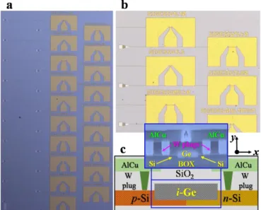
Fig. 1. Optical micrograph images of waveguide-integrated pin photodetectors with lateral silicon-germanium-silicon hetero-junctions: (a) Full array of devices and (b) close-up view of some structures. (c) Cross-sectional schematics of the photodetector with a lateral silicon-germanium-silicon heterojunction integrated at the end of the silicon-on-insulator waveguide. Light coming from an input strip waveguide is injected into the intrinsic Ge region perpendicularly to the schematics. Inset: Scanning electron microscopy image of a fabricated pin photodetector.
In this work, we comprehensively investigate the properties of optical photodetectors with lateral Si-Ge-Si heterojunctions.
All photodetectors are integrated at the end of conventional Si waveguides on 200 mm SOI substrates and are readily compatible with industrial-scale semiconductor manufacturing processes. Capitalizing on our previous efforts [39, 40], in this work, we provide a detailed experimental study of optical photodetectors of different waveguide geometries. The resulting Ge photodetectors exhibit promising opto-electrical performances in terms of dark-currents, responsivity, bandwidth and power consumption. Those devices are suitable for the future needs in high-speed links operating at 40 Gbps.
II. DESIGN, INTEGRATION AND FABRICATION
In this work, the Ge photodetectors, shown in Fig. 1, were integrated on top of regular SOI waveguide platforms, with 220 nm thick Si layer on top of 2 µm thick buried oxide (BOX) layer. As schematically illustrated in Fig. 1(c), the Ge photodetector is a pin diode structure (made of p-doped-type / intrinsic (i) / n-doped-type regions) at the end of the Si waveguide. The waveguide-integrated Si-Ge-Si pin photodetector consists in a Ge light-absorbing layer (intrinsic Ge zone, i-Ge) with a thickness of about 260 nm. The Ge layer is selectively grown in slits (with ~60 nm thick Si bottom layers just above the BOX) sandwiched between n-type and p-type doped Si slabs (p-Si and n-Si, respectively) with metal via contacts on top.
Surface grating couplers (Fig. 1(b)) were used to inject light from a standard optical fiber into the on-chip Si waveguides. A C-band wavelength (i.e. 1.55 µm) was selected and a transverse electrical (TE) waveguide mode evaluated. Strip waveguides were used for low-loss butt-coupling light injection into the Si-Ge-Si photodetectors. The input strip waveguides, 220 nm thick and 500 nm wide, were designed to preserve single-mode propagation. Light funneling into the Ge photodetector via the butt-coupling approach is a robust injection scheme with no further optimization needed, as the Ge intrinsic zone is in direct contact with the input waveguide. Devices were fabricated with a simplified process flow and conventional CMOS tools in CEA LETI’s cleanroom. We used 200 mm SOI wafers, with 220 nm thick Si layer on top of 2 µm thick BOX. The process was initiated by fabricating the passive devices such as fiber couplers and waveguides. The main process steps used were: (i) Si waveguide fabrication: cap layer formation, ion implantations and Si cavity formation; (ii) intrinsic Ge selective epitaxial growth, followed by passivation and insulation; and (iii) back-end-of-line standard CMOS metallization with tungsten (W-type) metal plugs and aluminum copper (AlCu) electrodes. The detailed description of the fabrication flow can be found in Refs. [39, 40]. Optical micrograph images of fabricated optical photodetectors are shown in Figs. 1(a) - full detectors array and 1(b) - enlarged view with a few devices and surface grating couplers. A cross-sectional Scanning Electron Microscopy image of a photodetector cross-section can be found in the inset of Fig. 1(c).
III. PHOTODETECTOR PERFORMANCE:RESULT AND DISCUSSION
In the following, we describe the various experimental characterization techniques and quantify the opto-electrical performances of our waveguide-integrated hetero-structured Si-Ge-Si pin photodetectors.
A. Leakage dark-current measurements
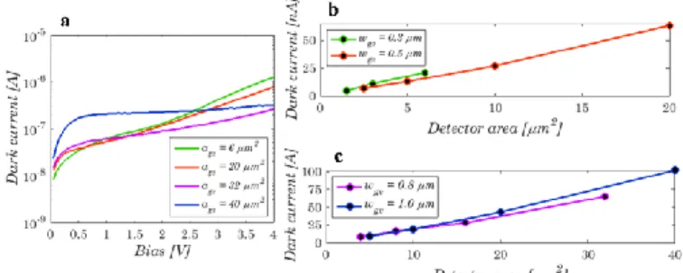
Dark-currents were evaluated through static current-voltage (I-V) measurements without light illumination, as a function of the applied reverse bias voltage for various waveguide-integrated photodetectors. Low-reverse-bias voltages were selected for device operation, as they do not degrade the opto-electrical performances in terms of responsivity and cut-off frequency response. Minimizing the operation bias is also desired for integration with CMOS circuitry. I-V tests were conducted on devices with different widths (wge) and lengths
(lge) of the intrinsic Ge zone. More specifically, Ge detector
widths of 0.3, 0.5, 0.8 and 1.0 µm and lengths of 5, 10, 20 and 40 µm were considered. Figs. 2 shows the best dark-current levels for the various photodetectors.
Fig. 2. (a) Conventional static current-voltage characteristics of hetero-structured pin photodetectors with different junction areas (age = wge × lge)
under dark-illuminated conditions. Ge detector widths of 0.3, 0.5, 0.8 and 1.0 µm and lengths of 5, 10, 20 and 40 µm were investigated. Evolution of the leakage dark-currents versus photodetector junction area under 1 V reverse bias voltage for Ge widths of (b) 0.3 µm and 0.5 µm, and (c) 0.8 µm and 1.0 µm, respectively.
Fig. 2(a) shows conventional dark-current curves for pin photodetectors with the largest Ge areas (age = wge × lge).
Under low-bias (in particular, at -1 V bias), dark-currents remain low, of the order of a few tens of nA only. The maximum dark-currents were consistently measured on the largest devices (age = 40 µm2), with values approaching 150
nA. The measured dark current levels are comparable [32, 33] or slightly higher than those achieved with other hetero-structured pin photodetectors [34-38], yet they are substantially lower than many pure homo-junction devices [19, 21, 22, 24, 26, 28, 30]. To reach the highest signal-to-noise ratio (SNR) possible, the dark-current levels should be as low as possible. As confirmed above, small-sized photodetectors favor low noise operation as dark-currents scale with the detector active volume. It is also worth to mention that conventional pin photodetectors operated under low-bias supplies are typically connected to additional receiver electronic circuits with a trans-impedance amplifier (TIA) and a limiting amplifier (LA) [30]. In those situations, the dark current is not a dominating noise source, as the input-referred noise of TIA is comparatively larger than the dark
current. Photodetectors presented in this work exhibit low dark current levels, typically well-below 1 µA. This is promising for the development of high-speed optical receivers based on group-IV nanophotonic platform. Indeed, the dark-current also directly increases with the reverse bias and/or the shrinking the intrinsic width of the Ge detector. The later trend is due to the stronger electric field within the intrinsic Ge zone, as for a given reverse bias the electric field increases as the intrinsic Ge region width decreases. As shown in Fig. 2(a), there is a significant increase of the dark-current with the electric field (age = 6, 20 and 32 µm2 devices). Meanwhile, the relatively
weak electric field present in the largest devices does not yield such bias dependence (age = 40 µm2 device). Figures 2(b) and
2(c) show that the dark-current leakage increases linearly with the detector area, this whatever the intrinsic width. All devices were biased with a 1 V reverse bias. The mean dark current densities for the smallest and the largest devices are in a range of 0.404±0.019 A/cm2 to 0.808±0.129 A/cm2, respectively.
The large dark current densities are attributed to the small junction area, as the Ge layer is only ~260 nm thick, and to the low to moderate dark current values.
B. Photo-responsivity measurements
To characterize the device responsivity (quantum efficiency), we performed additional I-V measurements, this time under light illumination. The light generated by a tunable laser source was injected from a single-mode optical fiber into the Si chip using surface grating couplers. Prior to coupling, a polarization controller was used to maximize the grating coupler transmission for TE-like waveguide mode and a central operating wavelength of 1.55 µm. The output power was monitored thanks to an optical power meter, with a measured level of about -11 dBm and an estimated uncertainty of ±0.25 dB. The device photo-responsivity (rp) was
calculated as follows [1]:
/
. c dc pc p p i i W A r (1)Here, ipc and idc stand for generated photo- and dark-currents,
respectively, and pc is the average optical power coupled into
the waveguide photodetector.
Fig. 3. Responsivities for a set of waveguide-integrated pin photodetectors with lateral silicon-germanium-silicon heterojunctions as functions of the applied reverse voltage. The measurements were conducted at a nominal wavelength of 1.55 µm. (a) Photodetectors with different junction areas (age =
wge × lge) and photodetectors with various lengths and widths of the intrinsic
Ge region: (b) wge = 0.3 µm and (c) wge = 1.0 µm. The measured photo-current
resulted from an average optical power injected in devices of about –11 dBm.
photodetectors with different geometries as functions of the applied reverse bias. Fig. 3(a) shows the evolution of the photo-responsivity for the largest device areas (age = wge × lge),
which have the following in-plane geometries: age = 0.3 µm ×
20 µm; 0.5 µm × 40 µm; 0.8 µm × 40 µm and finally, 1.0 µm × 40 µm. Meanwhile, Figs. 3(b) and 3(c) show device photo-responsivities for various Ge lengths, this for 0.3 µm- and 1 µm-wide devices.
Under 0 V bias, the responsivity of hetero-structured Si-Ge-Si photodetectors remains low, because of the weak built-in electric field. In particular, as shown in Fig. 3(a), for device junction areas of age = 0.3 µm × 20 µm; 0.5 µm × 40 µm; 0.8
µm × 40 µm, and finally, 1.0 µm × 40 µm, measured responsivities are equal to 0.14 A/W, 0.27 A/W, 0.47 A/W, and 0.63 A/W. As expected, the responsivity increases with the reverse voltage. This is due to a high electric field within the intrinsic Ge region of the photodetector. Such a behavior is also associated with a very fast and sharp responsivity increase. The responsivity maximum is typically reached at a low-bias voltage of -0.5 V. The extracted responsivities in Fig. 3(a) devices are substantially larger, then: 0.17 A/W, 0.44 A/W, 0.73 A/W, and 1.16 A/W. Excellent operation at low-bias shows that Si-Ge-Si pin photodetectors have a marked ability to sweep out the vast majority of electron-hole pairs within their lifetime. Indeed, high responsivities (>1 A/W) were also demonstrated in both full-Ge [19, 21, 22, 24, 25] and hetero-structured devices [32, 33, 35]. The responsivity increases with the width and the length of the intrinsic Ge region. Beyond 0.5 V reverse bias, responsivities reach a plateau for the largest devices, with a negligibly low or a moderate dependency on the applied reverse bias voltage. The evolution of the photo-responsivity with an applied bias is more pronounced in devices with narrower widths of the Ge intrinsic region. This can likely be attributed to the following, jointly acting, factors: (i) The built-in electric field, which is higher in narrow than in wide intrinsic regions, results in a higher voltage dependency. (ii) The increase of the electric field at the interface between the doped Si regions and the intrinsic Ge zone enables the E-field to penetrate in the Si regions, which can lead to collection of carriers generated within the Si-doped slabs and can also it initiate a local impact ionization process, producing a small gain of the generated current. (iii) A reduced modal confinement within the narrow intrinsic Ge region. The later aspect may decrease the absorption efficiency in Ge and increase adverse losses coming from the higher overlap between the TE-like waveguide mode and the heavily doped Si regions.
It is obvious, when looking at Fig. 3 data, that waveguide-integrated pin photodetectors with hetero-structured lateral junctions yield very high levels of quantum efficiency (η), approaching the theoretical limit of 100%. In other words, pin photodetectors built upon lateral Si-Ge-Si heterojunctions transform very efficiently incident photons into electrons and therefore photo-currents. The quantum efficiency is defined as follows [1]:
% 1.24 . rp (2)
Here, rp is the experimentally determined photo-responsivity
and λ is the reference wavelength of 1.55 µm. Similarly to device photo-responsivity, the quantum efficiency scales with the lengths and widths of the intrinsic Ge region. Quantum efficiency, at 1.55 µm wavelength and with 0.5 V reverse bias, is equal to 13.75% for age = 6 µm2, 35.1% for age = 20 µm2,
58.7% for age = 32 µm2, and 92.8% for age = 40 µm2.
C. Opto-electrical bandwidth assessments
The opto-electrical properties of Si-Ge-Si hetero-structured pin photodetectors have been investigated through small-signal radio-frequency (RF) measurements. A standard RF-test set-up and a commercial Lightwave Component Analyzer (LCA), including an internal laser source and a modulator, provided responses of the S21 parameter over the 0.1 GHz to
50 GHz range, the latter frequency being the upper limit of the LCA. Off-chip light coupling was done thanks to a fiber-chip surface grating coupler. The photodetectors under study were reversely biased via a bias-tee connected to a source measurement unit.
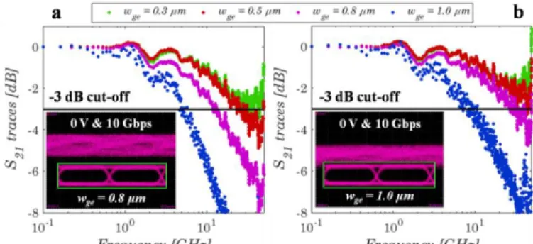
Fig. 4. Radio-frequency responses of the normalized S21 parameter for
waveguide-integrated pin photodetectors with different widths of the intrinsic Ge region under a reverse bias of (a) 1 V and (b) 2 V, respectively. Frequency measurements of S21 parameter were performed at a wavelength of 1.55 µm
with a power coupled into the photodetectors of about -11.4 dBm. Insets: Reference and retrieved eye diagrams for 0.8 µm- and 1 µm-wide devices under 0 V at a bit rate of 10 Gbps.
Figure 4 shows a collection of normalized S21 traces from
small-signal RF tests on hetero-structured pin photodetectors with different intrinsic zone geometries (wge / lge = 0.3 µm / 20
µm, 0.5 µm / 40 µm, 0.8 µm / 40 µm and 1.0 µm / 40 µm). Devices were biased at reverse voltages of 1 V (Fig 4(a)) and 2 V (Fig. 4(b)), respectively. The power coupled to the photodetectors was estimated to be -11.4 dBm. 10 Gbps eye diagrams (reference and retrieved) of 0.8 µm- and 1 µm-wide devices probed at 0 V bias are included in insets of Figs. 4(a) and 4(b), respectively. The reference diagrams correspond to optical input signals. Retrieved eyes remain closed due to the small -3 dB cut-off frequency. The extracted zero-bias -3-dB bandwidths are: 4.8 GHz, 2.8 GHz, 1.3 GHz, and 1.1 GHz respectively to the intrinsic Ge region dimensions given above. Such small cut-off responses are due to the long transit carrier time and the weak built-in electric field. This hinders the device ability to efficiently collect photo-generated pairs of electrons and holes under 0 V bias. Moreover, this is also in line with the low responsivities at 0 V.
In opposition, as shown by RF responses in Fig. 4, biasing at 1 V and 2 V considerably enhanced the -3-dB bandwidths
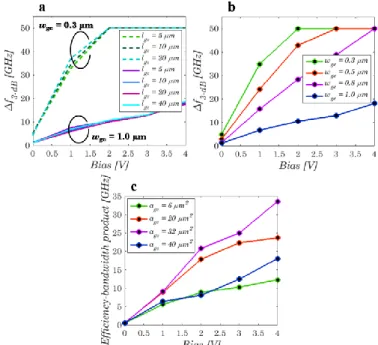
of pin photodetectors compared to reference bandwidths at 0 V bias. The -3-dB cut-off frequency also drastically increases as the photodetectors become narrower. Bandwidths for all tested devices as functions of the applied reverse bias are provided in Figs. 5(a) and 5(b), respectively. The extracted -3 dB bandwidths under a low-bias voltage of 1 V are equal to 35.0 GHz, 24.2 GHz, 15.7 GHz, and 6.7 GHz for 0.3, 0.5, 0.8, and 1.0 µm-wide intrinsic Ge regions. Fast responses achieved with our hetero-structured Si-Ge-Si devices well match the speed performances in the state-of-the-art full-Ge and hetero-structured photodiodes [17-38]. As shown in Fig. 5(a), the -3 dB bandwidth does not really depend on the length of the intrinsic Ge region (here, for a fixed device widths of 0.3 µm and 1.0 µm, respectively). Indeed, only marginal ripples were observed inside the measured bandwidth. This reveals that the bandwidth properties of the hetero-structured Si-Ge-Si photodetectors remain constant with the variation in device lengths and that the main bandwidth limitation is driven by the transit time.
Fig. 5. Opto-electrical bandwidth properties for different lengths (a) and widths (b) of the intrinsic Ge region. (c) Product of quantum efficiency and -3-dB opto-electrical bandwidth as a function of applied reverse bias voltage for different junction areas of the pin photodetectors with lateral silicon-germanium-silicon heterojunctions. The small-signal radio-frequency tests were carried out at a wavelength of 1.55 µm and the average optical power coupled to the devices was estimated to be -11.4 dBm.
Figure 5(c) shows the product of the quantum efficiency by the -3-dB optical bandwidth as a function of the applied reverse bias voltage for the largest Ge areas of hetero-structured pin photodetectors. These Ge areas are the same as before. The efficiency-bandwidth product provides a figure-of-merit suitable for photodetector design in terms of opto-electrical performance and footprint.
Device areas of 6 µm2 (the smallest one: w
ge = 0.3 µm and
lge = 20 µm) and 40 µm2 (the largest one: wge = 1.0 µm and lge
= 40 µm) result only in moderate opto-electrical performances. The former type of device enables fast operation (beyond 50 GHz, potentially). However, its
responsivity under 1 V bias is 0.19 A/W only (15.03% in quantum efficiency). Those values are not high enough to use in nanophotonics. Meanwhile, the latter detector layout has an outstanding responsivity to incident photons of 1.17 A/W (approaching 100% quantum efficiency). However, the device speed is lower and fundamentally restricted by the large cross-section, i.e. transit time limited operation.
As shown in Fig. 5(c), the best opto-electrical performances under a low-bias condition were achieved for 20 µm2 and 32
µm2 photodetector areas. The corresponding in-plane
dimensions of the Ge region are as follows: 0.5 µm x 40 µm and 0.8 µm x 40 µm. Both devices provide opto-electrical performances that fit for high-speed applications, including high-rate data networks, while their compact footprint allows a high density integration of multiple opto-electronic devices on a single Si chip. Their specific responsivities of 0.47 A/W and 0.76 A/W (37.7% and 60.84% in quantum efficiency) are coupled with fast responses of the order of tens of GHz.
D. Large-signal data link measurements
To assess the viability of waveguide-integrated pin photodetectors with lateral Si-Ge-Si heterojunctions in optical data links, we have also carried out large-signal measurements via detailed eye diagram inspections. To that end, data were transmitted in a non-return-to-zero (NRZ) modulation format. The pseudo-random-binary-sequence (PRBS) pattern of length 27 -1 was used for different data rates. Due to the frequency
limitation of the pattern generator, we could not provide high-speed tests beyond 40 Gbps. A DFB laser at a wavelength of 1.55 µm was modulated with an external modulator, followed by an optical amplifier, an optical filter, and a fibered coupler. One output of the coupler was connected to a 60 GHz photodiode of an oscilloscope to display the modulated respective input signal as a reference. The other output signal of the coupler was transmitted towards the device through an optical attenuator and an in-line power meter to control the optical power level. The polarization of the input light was controlled to match the TE-like mode of the Si waveguide and optimize the signal intensity. Finally, the signal was sent into the chip thanks to a fiber-to-chip surface grating coupler and detected by hetero-structured pin photodetectors, without the use of subsidiary electronic stages with trans-impedance amplifier or limiting amplifier. Electrical data were collected with a RF set-up and sent to the high-speed oscilloscope [40]. Figure 6(a) - 6(c) show eye diagrams for 40 µm-long pin photodetectors with different intrinsic Ge widths (1.0 µm, 0.8 µm, and 0.5 µm) under a 0.5 V reverse bias state and at a data rate of 10 Gbps. Reference 10 Gbps eye diagram aperture is shown in Fig. 6(d). In all cases, eye diagrams are clearly open under such conditions. Low-voltage operation is desirable to keep dark-currents as low as possible and be compatible with CMOS circuits. On the other hand, it is worth noting that simple pin photodiodes typically yield low electrical output levels. As a consequence, the implementation of trans-impedance amplifier with pin photodiodes is foreseen to be an essential step to access full transmission system assessments with the presented devices [30].
Besides low-bias operation and affordable high-speed transmission ability, the amount of energy consumed by each active device, in this case, an optical photodetector, is essential in an optical communication system design. The energy consumption, denoted here as ec, is estimated as follows [30]:
1
. pc ec fJ bit i v br (3)Here, br is the transmission bit rate, ipc is the measured current
(including photo- and dark-currents), and v is the reverse bias.
Fig. 6.Eye diagram apertures under low-reverse-bias of 0.5 V and a fixed data rate of 10 Gbps for 40-µm-long waveguide-integrated pin photodetectors with varying Ge intrinsic region widths: (a) 1.0 µm, (b) 0.8 µm, and (c) 0.5 µm. (d) Reference eye diagram for a bit rate of 10 Gbps. The power coupled into the photodetectors was estimated to be -8.9 dBm. Here, x [ps/div] and y [mV]/div are horizontal and vertical axes of the scope, respectively. (e) Calculated energy consumption per transmitted bit of the studied pin photodetectors as a function of the Ge intrinsic width under different reverse voltages and a fixed 10 Gbps optical link rate.
Figure 6(e) shows the evolution of the consumed energy versus the width of the intrinsic Ge region. Here, the pin Ge photodetectors were 40-µm-long and were probed under several reverse bias states (0.5 V, 1 V, and 2 V). The considered link data rate was 10 Gbps. We may state that wider Ge detectors yield higher energy consumption and that the increase consumption remains roughly proportional to the reverse voltage increase for each width. This trend is more perceptible under higher bias voltages. More specifically, under a 0.5 V bias point, doubling the width of the intrinsic Ge region (from 0.5 µm to 1.0 µm) yields moderate increase of consumed energy (from 3.1 fJ/bit to 7.7 fJ/bit), while under a 2 V bias state, this increase is from 11.5 fJ/bit to 31.2 fJ/bit. Nevertheless, in all cases, the energy consumption remains reasonably low, typically units or few tens of fJ/bit under low-bias states. This makes hetero-structured Si-Ge-Si pin photodetectors promising for use in energy-efficient Si-based optical interconnects.
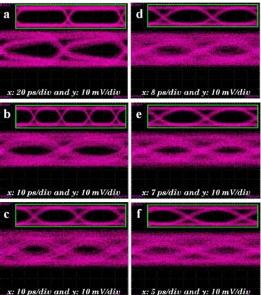
Fig. 7. Eye diagram apertures of 0.8 µm-wide by 40 µm-long pin photodetector under a 1 V reverse bias and an optical input power coupled into the device of -9 dBm. Large-signal data link inspections are performed for different data rates of (a) 10 Gbps, (b) 20 Gbps, (c) 25 Gbps, (d) 28 Gbps, (e) 32 Gbps, and (f) 40 Gbps. Insets: Reference eye diagrams. Here, x [ps/div] and y [mV]/div are horizontal and vertical axes of the scope, respectively.
Figure 7 shows the eye diagrams of a 0.8 µm-wide and 40 µm-long hetero-structured pin photodetector biased at -1 V for different transmission data rates, from 10 Gbps up to 40 Gbps. Reference eye diagram apertures are shown as insets in Fig. 7. Eye diagrams remain open, even for data rates beyond 25 Gbps, which is promising for the future on-chip detection of high-speed signal traffic. At a data rate of 40 Gbps, the pin photodetector operates in the voltage-limited regime, since the eye diagram begins to close. Indeed, the small-signal RF measurements have reported that the -3-dB bandwidth was around 16 GHz (under -1 V). This result explains the eye diagram aperture trends and perfectly agrees with performed large-signal optical link measurements. For 32 Gbps (see Fig. 7(e)), the eye diagram is still clearly open, while for 40 Gbps, it starts to have a closure. Moreover, energy consumption is predicted to be, for this photodetector and under a 1 V reverse bias, as low as 9.8 fJ/bit and 2.4 fJ/bit for 10 Gbps and 40 Gbps optical link rates, respectively.
IV. CONCLUSION
To summarize, we comprehensively studied the opto-electrical properties of waveguide-integrated pin detectors with lateral Si-Ge-Si heterojunctions. Such devices take full advantage of an easier integration scheme than that of Ge homo-junction photo-detectors. Such photodetectors are promising for use in nanophotonics as they are (i) built upon abundantly available materials, (ii) power-friendly and (iii) easily driven by low-voltage supplies, resulting in competitive
opto-electrical performances. They are promising for use in future energy-efficient 40 Gbps optical communication links.
REFERENCES
[1] L. Vivien and L. Pavesi, Handbook of Silicon Photonics, CRC Press, 2013.
[2] A. Alduino and M. Paniccia, “Wiring electronics with light,” Nature Photonics, vol. 1, pp. 153-155, 2007.
[3] M. Asghari and A. V. Krishnamoorthy, “Energy-efficient communication,” Nature Photonics, vol. 5, pp. 268-270, 2011. [4] A. Biberman and K. Bergman, “Optical interconnection networks for
high-performance computing systems,” Reports on Progress in Physics, vol. 75, 046402, pp. 1-15, 2012.
[5] C. Sun, M. T. Wade, Y. Lee, J. S. Orcutt, L. Alloatti, M. S. Georgas, A.S. Waterman, J. M. Shainline, R. R. Avizienis, S. Lin, B. R. Moss, R. Kumar, F. Pavanello, A. H. Atabaki, H. M. Cook, A. J. Ou, J. C. Leu, Y.-H. Chen, K. Asanovic, R. J. Ram, M. A. Popovic, and V. M. Stojanovic, “Single-chip microprocessor that communicates directly using light,” Nature, vol. 528, pp. 534-538, 2015.
[6] A. H. Atabaki, S. Moazeni, F. Pavanello, H. Gevorgyan, J. Notaros, L. Alloatti, M. T. Wade, C. Sun, S. A. Kruger, H. Meng, K. Al Qubaisi, I. Wang, B. Zhang, A. Khilo, C. V. Baiocco, M. A. Popovic, V. M. Stojanovic, and R. J. Ram, “Integrating photonics with silicon nanoelectronics for the next generation of systems on a chip,” Nature, vol. 556, pp. 349-354, 2018.
[7] F. Boeuf, C. Cremer, E. Temporiti, M. Fere, M. Shaw, C. Baudot, N. Vulliet, T. Pinguet, A. Mekis, G. Masini, H. Petiton, P. Le Maitre, M. Traldi, and L. Maggi, “Silicon Photonics R&D and Manufacturing on 300-mm Wafer Platform,” IEEE Journal of Lightwave Technology, vol. 34, pp. 286-295, 2016.
[8] A. Rahim, T. Spuesens, R. Baets, and W. Bogaerts, “Open-Access Silicon Photonics: Current Status and Emerging Initiatives,” Proceedings of the IEEE, vol. 106, pp. 2313-2330, 2018.
[9] D. Dai, J. Bauters, and J. E. Bowers, “Passive technologies for future large-scale photonic integrated circuits on silicon: polarization handling, light non-reciprocity and loss reduction,” Light: Science & Applications, vol. 1, e1, pp. 1-12, 2012.
[10] R. Halir, A. Ortega-Moñux, D. Benedikovic, G. Z. Mashanovich, J. G. Wangüemert-Pérez, J. H. Schmid, Í. Molina-Fernández, and P. Cheben, “Subwavelength-Grating Metamaterial Structures for Silicon Photonic Devices,” Proceedings of the IEEE, vol. 106, pp. 2144-2157, 2018. [11] D. Marris-Morini, V. Vakarin, J. M. Ramirez, Q. Liu, A. Ballabio, J.
Frigerio, M. Montesinos, C. Alonso-Ramos, X. Le Roux, S. Serna, D. Benedikovic, D. Chrastina, L. Vivien, and G. Isella, “Germanium-based integrated photonics from near- to mid-infrared applications,”
Nanophotonics, vol. 7, pp. 1781-1793, 2018.
[12] V. Reboud, A. Gassenq, J. M. Hartmann, J. Widiez, L. Virot, J. Aubin, K. Guilloy, S. Tardif, J. M. Fédéli, N. Pauc, A. Chelnokov, and V. Calvo, “Germanium based photonic components toward a full silicon/germanium photonic platform,” Progress in Crystal Growth and Characterization of Materials, vol. 63, pp. 1-24, 2017.
[13] Z. Zhou, B. Yin, and J. Michel, “On-chip light sources for silicon photonics,” Light: Science & Applications, vol. 4, e358, pp. 1-13, 2015. [14] G. T. Reed, G. Mashanovich, F. Y. Gardes, and D. J. Thomson, “Silicon
optical modulators,” Nature Photonics, vol. 4, pp. 518-526, 2010. [15] P. Chaisakul, D. Marris-Morini, J. Frigerio, D. Chrastina, M.-S. Rouifed,
S. Cecchi, P. Crozat, G. Isella, and L. Vivien, “Integrated germanium optical interconnects on silicon substrates,” Nature Photonics, vol. 8, pp. 482-488, 2014.
[16] J. Michel, J. Liu, and L. C. Kimerling, “High-performance Ge-on-Si photodetectors,” Nature Photonics, vol. 4, pp. 527-534, 2010. [17] S. B. Samavedam, M. T. Currie, T. A. Langdo, and E. A. Fitzgerald,
“High-quality germanium photodiodes integrated on silicon substrates using optimized relaxed graded buffers,” Applied Physics Letters, vol. 73, pp. 2125-2127, 1998.
[18] L. Colace, G. Masini, G. Assanto, H.-C. Luan, K. Wada, and L. C. Kimerling, “Efficient high-speed near-infrared Ge photodetectors integrated on Si substrates,” Applied Physics Letters, vol. 76, pp. 1231-1233, 2000.
[19] T. Yin, R. Cohen, M. M. Morse, G. Sarid, Y. Chetrit, D. Rubin, and M. J. Paniccia, “31 GHz Ge n-i-p waveguide photodetectors on Silicon-on-Insulator substrate,” Optics Express, vol. 15, pp. 13965-13971, 2007.
[20] L. Colace, P. Ferrara, G. Assanto, D. Fulgoni, and L. Nash, “Low dark-current germanium-on-silicon near infrared detectors,” IEEE Photonics Technology Letters, vol. 19, pp. 1813-1842, 2007.
[21] D. Ahn, C.-Y. Hong, J. Liu, W. Giziewicz, M. Beals, L. C. Kimerling, J. Michel, J. Chen, and F. X. Kärtner, “High performance, waveguide integrated Ge photodetectors,” Optics Express, vol. 15, pp. 3916-3921, 2007.
[22] L. Vivien, M. Rouvière, J.-M. Fédéli, D. Marris-Morini, J.-F.
Damlencourt, J. Mangeney, P. Crozat, L. El Melhaoui, E. Cassan, X. Le Roux, D. Pascal, and S. Laval, “High speed and high responsivity germanium photodetector integrated in silicon-on-insulator microwaveguide,” Optics Express, vol. 15, pp. 9843-9848, 2007. [23] L. Chen, P. Dong, and M. Lipson, “High performance germanium
photodetectors integrated on submicron silicon waveguides by low temperature wafer bonding,” Optics Express, vol. 16, pp. 11513-11518, 2008.
[24] D. Feng, S. Liao, P. Dong, N.-N. Feng, H. Liang, D. Zheng, C.-C. Kung, J. Fong, R. Shafiiha, J. Cunningham, A. V. Krishnamoorthy, and M. Asghari, “High-speed Ge photodetectors monolithically integrated with large cross-section silicon-on-insulator waveguide,” Applied Physics Letters, vol. 95, 261105, pp. 1-3, 2009.
[25] L. Vivien, J. Osmond, J.-M. Fédéli, D. Marris-Morini, P. Crozat, J.-F. Damlencourt, E. Cassan, Y. Lecunff, and S. Laval, “42 GHz p.i.n Germanium photodetector integrated in a silicon-on-insulator waveguide,” Optics Express, vol. 17, pp. 6252-6257, 2009.
[26] S. Assefa, F. Xia, S. W. Bedell, Y. Zhang, T. Topuria, P. M. Rice, and Y. A. Vlasov, “CMOS-integarted high-speed MSM germanium waveguide photodetector,” Optics Express, vol. 18, pp. 4986-4999, 2010.
[27] C. T. DeRoose, D. C. Trotter, W. A. Zortman, A. L. Starbuck, M. Fisher, M. R. Watts, and P. S. Davids, “Ultra compact 45 GHz CMOS compatible Germanium waveguide photodiode with low dark current,” Optics Express, vol. 19, pp. 24897-24904, 2011.
[28] L. Vivien, A. Polzer, D. Marris-Morini, J. Osmond, J. M. Hartmann, P. Crozat, E. Cassan, C. Kopp, H. Zimmermann, and J. M. Fédéli,, “Zero-bias 40Gbit/s germanium waveguide photodetector on silicon,” Optics Express, vol. 20, pp. 1096-1101, 2012.
[29] G. Li, Y. Luo, X. Zheng, G. Masini, A. Mekis, S. Sahni, H. Thacker, J. Yao, I. Shubin, K. Raj, J. E. Cunningham, and A. V. Krishnamoorthy, “Improving CMOS-compatible Germanium photodetectors,” Optics Express, vol. 20, pp. 26345-26350, 2012.
[30] H. Pan, S. Assefa, W. M. J. Green, D. M. Kuchta, C. L. Schow, A. V. Rylyakov, B. G. Lee, C. W. Baks, S. M. Shank, and Y. A. Vlasov, “High-speed receiver based on waveguide germanium photodetector wire-bonded to 90nm SOI CMOS amplifier,” Optics Express, vol. 20, pp. 18145-18155, 2012.
[31] L. Virot, L. Vivien, J.-M. Fédéli, Y. Bogumilowicz, J.-M. Hartmann, F. Boeuf, P. Crozat, D. Marris-Morini, and E. Cassan, “High-performance waveguide-integrated germanium PIN photodiodes for optical communication applications,” Photonics Research, vol. 1, pp. 140-147, 2013.
[32] Y. Zhang, S. Yang, Y. Yang, M. Gould, N. Ophir, A. E.-J. Lim, G.-Q. Lo, P. Magill, K. Bergman, T. Baehr-Jones, and M. Hochberg, “A high-responsivity photodetector absent metal-germanium direct contact,” Optics Express, vol. 22, pp. 11367-11375, 2014.
[33] S. Lischke, D. Knoll, C. Mai, L. Zimmermann, A. Peczek, M. Kroh, A. Trusch, E. Krune, K. Voigt, and A. Mai, “High bandwidth, high responsivity waveguide-coupled germanium p-i-n photodiode,” Optics Express, vol. 23, pp. 27213-27220, 2015.
[34] J. H. Nam, F. Afshinmanesh, D. Nam, W. S. Jung, T. I. Kamins, M. L. Brongersma, and K. C. Saraswat, “Monolithic integration of
germanium-on-insulator p-i-n photodetector on silicon,” Optics Express, vol. 23, pp. 15816-15823, 2015.
[35] H. T. Chen, P. Verheyen, P. De Heyn, G. Lepage, J. De Coster, P. Absil, G. Roelkens, and J. Van Campenhout, “High-Responsivity Low-Voltage 28-Gb/s Ge p-i-in Photodetector With Silicon Contacts,” IEEE Journal of Lightwave Technology, vol. 33, pp. 820-824, 2015.
[36] H. Chen, P. Verheyen, P. De Heyn, G. Lepage, J. De Coster, S. Balakrishnan, P. Absil, W. Yao, L. Shen, G. Roelkens, and J. Van Campenhout, “-1 V 67 GHz bandwidth Si-contacted germanium waveguide p-i-n photodetector for optical links at 56 Gbps and beyond,” Optics Express, vol. 24, pp. 4622-4631, 2016.
[37] H. Chen, P. Verheyen, P. De Heyn, G. Lepage, J. De Coster, S. Balakrishnan, P. Absil, G. Roelkens, and J. Van Campenhout, “Dark current analysis in high-speed germanium p-i-n waveguide
photodetectors,” Journal of Applied Physics, vol. 119, 213105, pp. 1-9, 2016.
[38] H. Chen, M. Galili, P. Verheyen, P. De Heyn, G. Lepage, J. De Coster, S. Bakakrishnan, P. Absil, L. Oxenlowe, J. Van Campenhout, and G. Roelkens, “100-Gbps RZ Data Reception in 67-GHz Si-Contacted Germanium Waveguide p-i-n Photodetectors,” IEEE Journal of Lightwave Technology, vol. 35, pp. 722-726, 2017.
[39] L. Virot, D. Benedikovic, B. Szelag, C. Alonso-Ramos, B. Karakus, J.-M. Hartmann, X. Le Roux, P. Crozat, E. Cassan, D. Marris-Morini, C. Baudot, F. Boeuf, J.-M. Fédéli, C. Kopp, and L. Vivien, “Integrated waveguide PIN photodiodes exploiting lateral Si/Ge/Si heterojunction,” Optics Express, vol. 25, pp. 19487-19496, 2017.
[40] D. Benedikovic, L. Virot, G. Aubin, F. Amar, B. Szelag, B. Karakus, J.-M. Hartmann, C. Alonso-Ramos, X. Le Roux, P. Crozat, E. Cassan, D. Marris-Morini, C. Baudot, F. Boeuf, J.-M. Fédéli, C. Kopp, and L. Vivien, “25 Gbps low-voltage hetero-structured silicon-germanium waveguide pin photodetectors for monolithic on-chip nanophotonic architectures,” Photonics Research, vol. 7, pp. 437-444, 2019. [41] A. Rahim, J. Goyvaerts, B. Szelag, J.-M. Fédéli, P. Absil, T. Aalto, M.
Harjanne, C. Littlejohns, G. Reed, G. Winzer, S. Lischke, L.
Zimmermann, D. Knoll, D. Geuzebroek, A. Leinse, M. Seiselmann, M. Zervas, H. Jans, A. Stassen, C. Dominguez, P. Munoz, D. Domenech, A. L. Giesecke, M. C. Lemme, and R. Baets, “Open-Access Silicon Photonics Platforms in Europe,” IEEE Journal of Selected Topics in Quantum Electronics, vol. 25, pp. 8200818, 2019.
ABOUT THE AUTHORS
Daniel Benedikovic received the M.Sc. degree in telecommunications and the
Ph.D. degree from the University of Žilina, Žilina, Slovakia, in 2011 and 2015, respectively. During his study, he completed several educational and scientific internships in Finland at Aalto University, in Spain at the University of Málaga, and in Canada at the National Research Council. He was a Nature Photonics award recipient at the IEEE International Conference on Group IV Photonics in 2014 in Paris, France. In 2015, he joined the Centre de Nanosciences et de Nanotechnologies, CNRS, Université Paris-Sud, Université Paris-Saclay in France, working as a post-doc Researcher. His current research activity mainly involves the development, design, and optical characterization of active germanium-based devices and various passive silicon nanophotonic components exploiting the sub-wavelength grating metamaterial structures.
Léopold Virot received the engineer degree in optics, lasers and plasma from
Orléans University and the Ph.D. degree from the Paris-Sud University, in France, in 2008 and 2014 respectively. He was a research engineer in a nanophotonics lab at CEA-Leti, France. In 2011, he started working toward his Ph.D. with STMicroelectronics and the Institut d’Electronique Fondamentale, studying Germanium on Silicon avalanche photodetectors. He received the Young Researcher Award from the Solid State Devices and Materials (SSDM) conference in 2014, in Japan. From 2015, he has been a Postdoctoral Researcher at CEA-Leti, France, working on the integration of Silicon Photonics technology for MEMS and NEMS based biosensing. Since 2018, he has been with CEA-Leti, France, where he is working as a researcher in the Silicon Photonics Integration Lab. His research activity mainly focuses on silicon based active and passive devices design, modeling and simulation for optical communications, quantum photonics and emerging applications.
Guy Aubin received the Engineer Diploma from Ecole Nationale Supérieure
des Télécommunications de Bretagne (now IMT Atlantique), Brest, France, and the MSc’s Degree in Information Processing from University of Rennes, France, both in 1981. He taught Electronics at university level during his National Service. He has been engaged in 1983 at Orange Labs (formerly France Télécom R&D or CNET). He was the head of the Transmission Experimentation Group at the Submarine Networks Department, Issy-les-Moulineaux. He contributed to several world premieres of optical transmission demonstrations in laboratory and to field trials of successive generations of optical systems. He moved in 1999 to the Concept and Device for Photonics Laboratory, Bagneux. In 2001 he joined the Centre National de la Recherche Scientifique at Marcoussis in the Laboratory for Photonics and Nanostructures whose structure has been now included in the Centre of Nanoscience and Nanotechnology, Marcoussis, since 2016. There he leads the Experimentations Fiber Optic and RF team. His research interests include new functionalities for next-generation communication networks with innovative all-optical or opto-electronics device.
Jean-Michel Hartmann explored, during his PhD in CEA-IRIG, Grenoble
(France), the atomic layer epitaxy of CdTe, MnTe and MgTe for low dimensional structures (1994-1997). During his stay in Imperial College, London (1997 – 1999), he investigated the gas source molecular beam epitaxy of Si/SiGe heterostructures for transport purposes. Since 1999, he is a permanent position researcher in CEA-LETI, Grenoble, where he is currently coordinating group-IV epitaxy activities for nanoelectronics and photonics.
Farah Amar received the Master degree in telecommunications and RF from
Limoges University, Limoges, France in 2016. In 2017, she joined the Centre for Nanoscience and Nanotechnology (C2N), a joint Laboratory of CNRS, University of Paris Sud and University of Paris Saclay, France. She works as RF and optoelectronic engineer in the EXPERFO team (Experimentations Fiber Optic and RF).
Bertrand Szelag received the Master degree in Physics from the University
of Lille in 1994 and the PhD degree in Microelectronics from the University of Grenoble in 1999. He has been a visiting researcher in Tohoku University in 1997 working in the field of sub-100nm CMOS transistor properties. In 1998 he joint Thomson Composants Specifiques. In 1999, he moved to STMicroelectronics to work on BiCMOS platform development for Analog/RF applications. He also developed devices for RF power applications. Since 2013, he has been with the LETI, MINATEC Institute, Grenoble, France as a Project Manager and senior process integration researcher in the field of silicon photonic devices. His current research activities included high speed silicon modulator, germanium photodetectors and hybrid III-V laser integration in silicon. He is now the head of the silicon photonic laboratory of CEA-LETI. He is the author or co-author of more than 50 papers in scientific journals and international conference proceedings in the field of CMOS, Bipolar and DMOS transistors and silicon photonic devices.
Xavier Le Roux joined the National Center of Scientific Research (CNRS) as
an Engineer in 2004. He is currently working on development and optimization of technological process dedicated to photonics applications and MEMS/NEMS.
Carlos Alonso-Ramos obtained his PhD in June 2014 at the Universidad de
Málaga, Spain, on the development of high-performance integrated photonic circuits for chip interconnects and next generation coherent transceivers. Currently, he is a CNRS researcher in the Center for Nanoscience and Nanotechnology (C2N) in Palaiseau, France. His research interest include the development of Si photonics devices and circuits in the near- and mid-infrared for applications in telecom, sensing and quantum.
Paul Crozat graduated at Ecole Normale Supérieure de St Cloud (1972) and
received the Doctorat-es-Sciences degree from Université Paris Sud in 1980. He worked on coherent Josephson type phenomena in niobium implanted superconducting microbridges and their high frequency and noise properties. He turned in 1980 to the picosecond properties of Josephson junctions and circuits with emphasis on propagation phenomena in fast circuits. Since 1983, he extended these modeling and measurement studies to III-V GaAs semiconductor picosecond circuits. He works now on RF, HF, THz and opto-electronic measurements on various devices at room and at low temperature with emphasis on noise. He has coauthored more than 150 journal papers. Since 2014 he is Professor emeritus at Paris-Sud University.
Éric Cassan has been a professor at the University of Paris-Sud since 2009.
His research topics concern silicon photonics, with a recent shift towards hybrid photonics on silicon for the realization of integrated optical sources and non-linear functions based on 3rd order nonlinear effects.
Delphine Marris-Morini is a Professor at Paris Sud University. Her research
interests at the Center for Nanosciences and Nanotechnologies include silicon photonics in the near-IR and mid-IR wavelength range. She received an ERC starting grant (INsPIRE) on Ge-rich photonic integrated chips towards the mid-IR wavelength range for sensing and spectroscopic application. She received the bronze medal from CNRS in 2013. She published over 100 journal papers and she is in charge of the group of Micro and Nanophotonic devices on silicon since 2015.
Charles Baudot received the M.Sc. degree in microelectronics from
Université Pierre et Marie Curie, Paris, France, in 2004, and the Ph.D. degree from Nanyang Technological University, Singapore, in 2010. In 2005, he joined STMicroelectronics, Singapore, as an R&D Engineer to explore alternative technologies to silicon. In the course of that activity, he worked on
molecular electronics, carbon nanotube based electronics, and printed electronics. In 2010, he joined STMicroelectronics, Crolles, France, as an Advanced R&D Senior Staff Engineer, where his activity is devoted to the development of advanced silicon photonic device and process integration.
Frédéric Boeuf was born 1972. He obtained his M.Eng. and M.Sc. degree
from Institut National Polytechnique de Grenoble in 1996 and Ph.D. from the University Joseph Fourier of Grenoble (France) in 2000. Then he joined STMicroelectronics working on Advanced Devices Physics and Integration, first on advanced CMOS devices then on Silicon Photonics. He authored and co-authored over 250 technical papers. Dr. Boeuf is currently STMicroelectronics Fellow and is managing the Silicon Photonics Technologies group inside STMicroelectronics’s Technology and Design Platform organization.
Jean-Marc Fédéli received his electronics engineer diploma from INPG
Grenoble in 1978. Then he was involved at CEA-LETI in the development of various magnetic memories and magnetic components as project leader, group leader, and program manager. For two years, he acted as advanced program director in Memscap Company for the development of RF-MEMS, then he returned to CEA-LETI in 2002 as coordinator of silicon photonic projects up to 2012. Under a larger research partnership, he works on many technological aspects on photonics on CMOS (Si rib and stripe waveguides, a-Si waveguides, slot waveguides), Si modulators, Ge photodetectors, InP integrated sources on Si. He has been participating on different European projects such as EPIXFAB for MPW circuit fabrication and has coordinated the FP7 PLAT4M project on Silicon Photonics Platform. Since 2014, he has moved to sensing activities with photonics and he is currently the technical manager of the H2020 MIRPHAB pilot line on liquid and gas systems sensors. His H factor is around 35 with more than 200 publications and 50 patents. He wrote three book chapters (one on magnetic recording and two on silicon photonics).
Christophe Kopp received the Ph.D. degree in photonic engineering from the
University of Strasbourg, Alsace, France, in 2000, in the field of diffractive optics. Since 2001, he has been with the CEA, LETI, MINATEC Institute, Grenoble, France, where he is involved in developing microoptoelectronic devices. He has been involved in several national and European collaborative projects mainly focused on high-speed optical communication technologies (ODIN, HELIOS, WADIMOS MICROS, SILVER, MINAPACK). In connection with industrial companies (Intexys Photonics, IIIV-lab Mapper lithography), he has been responsible for several R&D projects. He is the author or coauthor of more than 30 papers in scientific journals and international conference proceedings, one scientific book, and more than 30 patents. He is currently the Head of the Laboratory of CMOS Photonics with 30 Research Engineers/Technicians and six Ph.D. students.
Laurent Vivien is CNRS Director of Research at the Centre for Nanoscience
and Nanotechnology (C2N), a joint Laboratory of CNRS, University of Paris Sud and University of Paris Saclay, France. Since 2016, he has also served as Deputy Director of C2N and Director of the Photonics Department. His research activities focus on the development of fundamental concepts for silicon photonics including optoelectronic and hybrid photonic devices. Especially, he demonstrated high-speed waveguide integrated germanium photodetectors and carrier depletion based silicon modulators. He has also been at the forefront of the development of hybrid integration of carbon nanotubes on Si photonics platform and recently on high-speed Pockels effect in strained silicon waveguides. In 2015, he received the European Research Council (ERC) grant as consolidator on the development of strained silicon photonics platform.