Control and Current Sensing Systems for the
Parallel Resonant Pole Inverter Architecture
by
Henrik Martin
Submitted to the Department of Electrical Engineering and
Computer Science
in partial fulfillment of the requirements for the degree of
Master of Science in Computer Science and Engineering
at the
MASSACHUSETTS INSTITUTE OF TECHNOLOGY
May 1994
@
Henrik Martin, MCMXCIV. All rights reserved.
The author hereby grants to MIT permission to reproduce and to
distribute copies
of this thesis document in whole or in part, and to grant others the
right to do so.
I k'
A uthor
...
.. ...
DepartI
ent of Electrical Engineering and Computer Science
/
/
,
/
/
May 13, 1994
Certified by..
John G. Kassakian
Professor
2
-Accepted by ...
.
Chairmal,
Thesis Supervisor
... ...oic R. Morgenthaler
Graduate Students
Control and Current Sensing Systems for the Parallel
Resonant Pole Inverter Architecture
by
Henrik Martin
Submitted to the Department of Electrical Engineering and Computer Science on May 13, 1994, in partial fulfillment of the
requirements for the degree of
Master of Science in Computer Science and Engineering
Abstract
This thesis explores two important issues in the development of the Parallel Resonant Pole Inverter (PRPI) architecture, namely the current sensing and control systems. A reliable, robust and yet inexpensive control system is designed and developed, and five different current sensing systems are designed, developed and compared. The thesis also presents the design of a Resonant Pole Inverter (RPI), and highlights many of the issues involved in designing such a system.
Thesis Supervisor: John G. Kassakian Title: Professor
Acknowledgements
Five years at MIT is now coming to an end. They say your college years are supposed to be the best years in your life, and that has certainly been true for me.
The work related to my Master's Thesis has been incredibly rewarding. I would like to thank my thesis advisor, Professor John G. Kassakian, for providing the guide-lines, facilities, and support for my work. I also greatly appreciate the funding pro-vided by the Leader's for Manufacturing (LFM) Program. The best part of my experience as a graduate student, however, was to have the opportunity to work with Dave Perreault. Dave supervised my work, supported me during those long nights of debugging, taught me EE design, and became a great friend and companion. Dave: You are a truly exceptional person. Without your help, this thesis would never have been written, and for this I will forever be indebted to you.
Everybody else in LEES also deserves to be mentioned for making this a mem-orable experience. I am especially grateful to Vivian for helping out with all the administrative stuff: You're the best! Special thanks go to Tracy, Ahmed, Kamakshi, Joaquin, Niels, Mo, John, and Andres.
Without friends life would be unbearable. I would like to thank Mats, Lisa, and Matilda for being there. Petter and Mattias for being Swedish, guaranteed to be pals for life. MIT UNIHOC Club for all the work-outs. Nu Delta for being Nu Delta, the place where I learned to respect people for who they are. And of course, Mark, Marc, John, Andres, Brian, Paul, Soykan, Al, Andy, and all the other people I was fortunate enough to meet.
Finally, I must mention my family. Despite being away for five years, I feel closer than ever to them. Pappa, Mamma, Peter+Ulrika+Julius, Robert: TACK! I am
really looking forward to seeing more of you in the future.
To my Christine, I dedicate this thesis. You are the best thing that ever happened to me, and I look forward to spending the rest of my life with you.
Contents
1 Introduction
12
2 The Parallel Resonant Pole Inverter Architecture
14
2.1
Introduction .. .. ...
14
2.2 The Resonant Pole Concept ...
14
2.3
The Paralleling of RPI's ...
18
2.4 Conclusion. ....
...
.
. ...
... ..
20
3 The Control System
21
3.1
The Control Strategy ...
21
3.2
The Control System Design ...
24
3.3
The Set-up for Testing the Control System . ...
26
3.4 Testing the Control System ...
27
4 The RPI System
34
4.1 Introduction ...
34
4.2
The Power Supply
...
34
4.2.1
Sizing the Capacitor ...
35
4.2.2
Sizing the Resistors ...
..
37
4.2.3
Sizing the Heatsink ...
37
4.3 The Inverter ...
...
... ..
39
4.3.1
Zero Voltage Detection ...
40
4.4 The Load ...
...
..
42
5 Current Sensing
43
5.1
Introduction ...
43
5.2 The Hall Effect Sensor ...
.43
5.2.1
Introduction . .
...
...
. . . . ...
43
5.2.2
Testing the Hall-Effect Sensor . . . .
45
5.2.3
Conclusion ...
.47
5.3
The Current Transformer ...
.49
5.3.1
Introduction ...
.49
5.3.2
Designing the Current Transformer . . . .
52
5.3.3
Designing the Resetting Mechanism . . . .
55
5.3.4
Testing the Current Transformer
. . . .
57
5.3.5
Conclusion ...
...
60
5.4 Resistive Current Sensing ...
.61
5.4.1
Introduction ...
.61
5.4.2
Designing the Sense Resistor . . . .
62
5.5
The Rogowski Coil ...
63
5.5.1
Introduction ...
. . .
...
...
63
5.5.2
Designing the Rogowski Coil System . ...
64
5.5.3
Designing the Rogowski Coil ...
69
5.5.4
Designing the Resetting Mechanism . ...
71
5.5.5
Testing the Rogowski Coil System . . . .
...
. . . . .
74
5.5.6
Conclusion . . . .
...
. . . .
76
5.6 The Second Winding ...
.
77
5.6.1
Introduction . . . .
.. .
. .
. . . .
77
5.6.2
Designing the Second Winding System . . . .
79
5.6.3
Testing the Second Winding Approach . ...
81
5.6.4
Conclusion ...
...
...
85
5.7 Conclusion ...
.
.. ...
...
...
...
...
86
A Inverter Module Description for the Testing of the Control System 89
B The Emulated Zero Voltage Crossing Detection
92
List of Figures
2-1 The resonant pole inverter and its switching waveform
. ...
15
2-2 An operational cycle of the Resonant Pole Inverter . ...
16
2-3 The parallel resonant pole inverter architecture. . ...
18
2-4 A resonant pole inverter leg and its equivalent parallel resonant pole
components ...
...
19
3-1
Illustration of basic hysteresis control. . ...
. .
22
3-2 The RPI Modulation Strategy ...
23
3-3 Block diagram of the control system . ...
23
3-4 Schematic for the control system
. ...
.
25
3-5 Test Set-up for developing the control system . ...
27
3-6 Picture of the High and Low signals output by the DG509 ...
28
3-7 The solid waveform shows the High signal (the upper hysteresis limit)
coming out of the DG509, while the switching waveform is the fedback
current . . . .
. . . .. .. .
29
3-8 Demonstration that the current switches at the upper hysteresis
bound-ary. The solid waveform shows the High signal coming out of the
DG509, while the switching waveform is the fedback current. ...
29
3-9 Output waveform as measured by a current probe attached just before
the load resistor R
1in Fig. 3-5. The scale is 2A/div. . ...
30
3-10 Three inverter cell output waveform as measured by a current probe
attached right after the joining node of the output inductors in Fig.
3-5. The scale is 5A/div ...
31
3-11 The current going into the filter capacitor for three inverter cells
oper-ating in parallel. The scale is set to 2A/div. . ... 32
3-12 Output waveform as measured by a current probe attached just before the load resistor R1. The scale is set to 5A/div. .. ... . . . .. . 32
4-1 Schematic of power supply ... 35
4-2 Illustration of the variations in bus capacitor voltage over time . . .. 36
4-3 The thermal system used for modeling the rectifier device, the device casing, and the heat sink. ... 38
4-4 Schematic of the RPI inverter . . . . 39
4-5 Schematic of the zero voltage detection system. . ... . 41
5-1 The Hall effect sensor. ... .44
5-2 The setup for testing the current sensing systems. . ... . . 45
5-3 Output waveform for Hall-effect sensor (top waveform) as compared to a current probe measurement (bottom waveform). The setting is 2A/div, and the switching frequency 85.5kHz. . ... 46
5-4 Output waveform for Hall-effect sensor (contains some switching noise) as compared to a current probe measurement (clean) at a high switch-ing frequency. The settswitch-ing is 1A/div and the switchswitch-ing frequency is 60kHz . . . .. . . . .... .. 47
5-5 Output waveform for Hall-effect sensor (lower trace) as compared to a current probe measurement (upper trace) at a low switching frequency. The setting is 5A/div and the switching frequency is 13.3kHz ... 48
5-6 The current transformer and its reset mechanism. . ... . . . 49
5-7 A model for the transformer ... 49
5-8 The placement of the current transformers . ... 51
5-9 Implementation of the resetting voltage . ... 55
5-11 Output waveform for current transformer (bottom waveform) as com-pared to a current probe measurement (top waveform) at a high switch-ing frequency. The settswitch-ing is 2A/div and the switchswitch-ing frequency is
84.7kH z . . . . .. . . . ... .. 58
5-12 Output waveform for current transformer (noisy, cutoff waveform) as compared to a current probe measurement (clean, full waveform) at low current levels. The setting is 1A/div and the switching frequency is 60kH z .. . . . . .. . . . .. .. 59
5-13 Output waveform for current transformer (cutoff waveform) as com-pared to a current probe measurement (complete waveform) at a low switching frequency. The setting is 5A/div and the switching frequency is 13.3kH z .. . . . .. . . . .. . .. 59
5-14 Oscilloscope picture showing the resetting mechanism. The top wave-form shows the current measured by the CT, displayed at 5A/div. The bottom waveform shows the voltage measured at the CT terminals at 2V/div. ... .. 60
5-15 The resistive current sensing system. . ... 62
5-16 Rogowski Coil System ... 65
5-17 The Rogowski coil and its Thevenin equivalent. . ... . 67
5-18 The circuit that shifts the zero voltage detection signals to the level required to operate the 2N3972 appropriately. . ... 73
5-19 Output waveform for Rogowski coil (top waveform) as compared to a current probe measurement (bottom waveform) at a high switching frequency. The setting is 2A/div and the switching frequency is 85.5kHz. 74 5-20 Output waveform for Rogowski coil (lower waveform) as compared to a current probe measurement (upper waveform) at a low current level. The setting is 1A/div and the switching frequency is 65kHz. ... 75
5-21 Output waveform for Rogowski coil (lower waveform) as compared to a current probe measurement (upper waveform) at a high current level. The setting is 5A/div and the switching frequency is 14kHz. ... 75
5-22 Oscilloscope picture showing the Rogoswski coil resetting mechanism. The top waveform shows the gate drive to the 2N3972, and the bottom
waveform shows the Rogowski coil output waveform. . ... 76
5-23 The second winding current sensing system . ... 78
5-24 Output waveform for second winding sensor (top waveform) as com-pared to a current probe measurement (bottom waveform). The setting
is 2A/div, and the switching frequency 80kHz. . ... . 82
5-25 Output waveform for second winding sensor (upper waveform) as com-pared to a current probe measurement (lower waveform) at a low cur-rent level. The setting is 1A/div and the switching frequency is 60kHz. 83 5-26 Output waveform for second winding sensor (upper waveform) as
com-pared to a current probe measurement (lower waveform) at a high current level. The setting is 5A/div and the switching frequency is 14kH z . . . .. . . . .... .. 83 5-27 Output waveform for second winding sensor (upper waveform) as
com-pared to a current probe measurement (lower waveform) at a low cur-rent level after the inductance of the output inductor has been adjusted. The setting is 1A/div and the switching frequency is 50kHz. ... 84 5-28 Output waveform for second winding sensor (upper waveform) as
com-pared to a current probe measurement (lower waveform) at a high current level after the inductance of the output inductor has been ad-justed. The setting is 5A/div and the switching frequency is 14.9kHz. 85
A-1 Block diagram of inverter leg ... .... 90
A-2 Bridge leg of inverter ... 91
B-1 The emulation of zero crossing detection signals . ... 93
List of Tables
3.1
Summary of the High and Low hysteresis bands signals. ...
.
22
4.1
Specifications for the RPI ...
34
4.2 Information about the rectifier available from the manufacturer . . . 38
5.1
Summary of the findings for the Hall-effect sensor. . ...
. .
48
5.2 Summary of the findings for the current transformer. . ...
61
5.3 Summary of the design parameters for the Rogowski coil...
71
5.4
Summary of the logic signals required to operate the JFET. ...
72
5.5
Summary of the findings for the Rogowski coil...
77
5.6
Summary of the design parameters for the second winding approach.
81
5.7 Summary of the findings for the second winding. . ...
86
Chapter 1
Introduction
The paralleling of low power inverter cells to form a high power converter system has substantial potential advantages over single cell designs. Some of these advantages, as outlined in [1], are:
1. Multiple inverters offer a possibility for redundancy, useful in applications where reliability is of importance.
2. For a given input voltage level and efficiency, smaller inverters, processing only a fraction of the full power, can usually be switched at a higher frequency than a large inverter processing full power. This results in a better waveform quality for the smaller units, leading to smaller filters required to filter the output signal. 3. The techniques of mass production and economies of high volume might reduce
the cost per kW, possibly making the paralleling of inverter cells very attractive from an economic point of view.
4. In the case of an inverter cell failure, the cell can easily be replaced without interrupting the power supply, improving the mean time to repair the system and therefore its availability.
5. The heat dissipated in the system will not be localized in one place, but rather shared by several physically separate units. This may reduce the level of com-plexity and cost required for the cooling system.
The idea of parallel inverter cells has been successfully implemented in the realm where very high power is required, such as in large AC motor drives [2] [3]. Another realm where paralleled converter systems have excelled is where a high degree of reliability is needed, as is the case in uninterruptible power supply systems [4][5] [6]. However, in the realm where mass production manufacturing techniques and high frequency switching are available, the potential benefits of a paralleled converter system are yet to be realized. In order to capture the potential benefits of the parallel architecture, the design issues of converter topology and control techniques must first be appropriately addressed. It is the purpose of this thesis to examine current sensing and control in a parallel inverter architecture.
Most components in a paralleled system are equivalent to a redistribution of larger components in a single inverter system. In other words, an inductor in a single inverter system can, in a parallel converter system with N cells, be redistributed as N inductors where each one is N times the inductance of the single inverter inductor. There are, however, two important exceptions to this argument: the control system and the current sensing system do not scale with increasing modularity. For every additional cell that is attached to the parallel system, an additional control system as well as current sensing system are required. It is therefore important to design these subsystems in the most inexpensive and yet reliable fashion.
There are two purposes for this work. The first purpose is to design and test an accurate, robust and yet inexpensive control system. The second purpose is to develop and compare five different schemes for sensing current, resulting in a recommendation as to which system is most appropriate for this particular parallel architecture. In order to perform all the necessary experiments, single and parallel inverter systems are constructed.
Chapter 2
The Parallel Resonant Pole
Inverter Architecture
2.1
Introduction
In recent years, much research in the area of switching power converters has focused on topological issues. One class of topologies which has gained increased attention is the soft switching inverter. Soft switched inverters are designed to reduce device switching losses by switching the devices only at zero voltage or zero current. This leads to a reduction in switching losses, allowing the devices to be operated at a much higher switching frequency. Resulting advantages over hard switched inverters include smaller component size, higher power density, higher efficiency, lower acoustic noise and low EMI.
2.2
The Resonant Pole Concept
The resonant pole inverter (RPI) is one member of the soft switching inverter fam-ily. Despite the advantages over hard switched converters, the RPI has not met with general approval due to drawbacks such as high rms current stresses on the fil-ter capacitors and the difficulty of constructing resonant elements using off-the-shelf components at high power levels. The parallel resonant pole inverter (PRPI)
architec-S2
1
Figure 2-1: The resonant pole inverter and its switching waveform
ture, however, possesses all the positive characteristics of an RPI, while eliminating
the two abovementioned limitations of the resonant pole topology.
The RPI is very well suited to the parallel architecture because of its simplicity,
small component size, and ability to operate at elevated switching frequencies [7]. In
addition to the power devices, it consists of a pair of resonant capacitors,
CR1and
CR2, and a resonant inductor, LR as shown in Fig. 2-1. The switching waveform
displayed in Fig. 2-1 shows that the control system is fundamentally hysteretic, with
large hysteresis bands around the reference current. A complete description of the
switching waveform and the control system is given in chapter 3.
An operational cycle of a single resonant pole inverter is shown in Fig. 2-2. A
basic assumption underlying the following analysis is that the output filter capacitor
is large enough to clamp the output voltage for the duration of the entire cycle. In
the first picture, designated as mode 1 in Fig. 2-2(a), only the top switch (Sl) is
conducting. The resonant inductor current builds up linearly because the voltage
across L, is constant at Vdc/2. The current will continue to ramp up until it reaches
a predetermined value ip+ set by the controller. At this point, S1 is turned off at
zero voltage since the device voltage is clamped by the resonant capacitor CR1, and
P-S2
(a) Mode 1 (b) Mode 2
71
1
L
iL A-I-I
(c) Mode 3 (d) Mode 4 L(e) Mode 5 (f) Mode 6
Figure 2-2: An operational cycle of the Resonant Pole Inverter
F- ~II II
r r\
r r ~ I
I I
--the circuit enters mode 2 in which --the resonant inductor, L,, rings with --the two resonant capacitors, as shown in Fig. 2-2(b). This ringing will continue until D2, the bottom diode, starts conducting and operation enters mode 3, as shown in Fig. 2-2(c). During mode 3, the lower main device, S2, may be turned on at zero voltage, since the diode D2 is conducting. The current through the resonant inductor Lr decreases linearly and eventually reverses, causing S2 to carry the current. At this time the circuit enters mode 4, shown in Fig. 2-2(d). When iL reaches a minimum value i,_ determined by the controller the bottom switch is turned off at zero voltage (the device voltage is clamped by the resonant capacitor CR2), and the bus now rings up in mode 5, as shown in Fig. 2-2(e). The ringing continues until the upper diode, D1, starts conducting, at which time the operation enters mode 6. In this final mode, the top switch may be turned on, again at zero voltage, and circuit operation is back in mode 1. The cycle is then repeated.
The switching frequency of an RPI varies dynamically, as it does for a standard hysteresis-controlled PWM system. On the basis of the assumption that the reso-nant transitions are short and do not significantly affect the inductor current, the instantaneous switching period can be expressed as:
T
= VdcL,(ip+ + ip-)(2.1)
0.25Vc - V2
The constraints on the values of i,+ and i,_ stem from the necessity of having enough energy stored in the inductor to ring the resonant capacitor voltages to zero in order to ensure zero-voltage switching. With ideal components, the minimum inductor current required at the end of mode 1 for a positive voltage Vcf can be expressed as:
imin = 2
Vcf
L
(2.2)
No current is required for the case when Vef is smaller than or equal to zero. Similarly, at the end of mode 4, the magnitude of i,_ must exceed iin for a negative Ve1 if the
bus is to ring appropriately, but may be zero in the case where Vc, is larger than or equal to zero.
L rl **O* V dc/2 V dc/2
Figure 2-3: The parallel resonant pole inverter architecture.
2.3
The Paralleling of RPI's
The paralleling of multiple inverter cells raises several concerns. One is that a current sharing mechanism must be implemented in order to prevent individual converters from exceeding their power rating. An illustration of the parallel resonant pole in-verter architecture is shown in Fig. 2-3. Current sharing is achieved through the use of a suitable control system combined with inductors at the cell outputs which absorb the instantaneous voltage difference between inverter cells. The inductors are added to the output of each individual inverter cell, as shown in Fig. 2-3. The output inductors make each inverter cell behave as a current source for times on the order of the switching period. The design of the output inductors is very important, since the inductors can make a significant contribution to a converter's overall cost and size.
The paralleling of RPI's has many advantages. As [8] shows, the PRPI results in minimum output magnetics, which, from the argument above, is very important. The PRPI requires only a simple control system, and can operate at higher frequencies than can a single large inverter due to the availability of high-performance devices,
Cr at Vdc Si AIN ... ... L r at i 1 ... max ARAM---** N x Si r at Vdc Si IN /N
Figure 2-4: A resonant pole inverter leg and its equivalent parallel resonant pole components
distribution of heat generation, and the reduction of parasitics [7]. It also eliminates two major drawbacks of the single RPI. The practical size of an RPI is often limited by the difficulty of constructing output inductors with sufficiently large ratings using off-the-shelf components [9]. With a PRPI, however, this is no longer necessarily a limitation. To see this, consider Fig. 2-4. An N cell PRPI can be constructed which is functionally equivalent to a single RPI with N times the power rating. An equivalent PRPI has, to first order, the same device area, resonant component energy storage and losses as a single RPI, while each inverter cell operates at the same frequency as the original. By distributing the inductance, the inverter becomes much more manufacturable, and is not limited in size by the output inductors.
Another major drawback of the resonant pole inverter is the high current stresses on the output filter capacitors, as discussed in [10]. This drawback is again alleviated by the PRPI architecture. Basically, significant ripple cancellation occurs among the individual inverter cells, reducing the rms current stress significantly on the filter capacitors, compared to a single large inverter. This occurs even with independent open loop control of individual cells, as is shown in [8]. Current stresses on the output filter capacitors can be reduced even further using active ripple cancellation or an interdependent control system.
2.4
Conclusion
The PRPI architecture is a very promising addition to the area of inverter topologies.
It retains all the advantages of the single RPI while eliminating many of the
draw-backs. However, in order to make the PRPI economically feasible, careful analysis of
its current sensing and control system is necessary.
Chapter 3
The Control System
3.1
The Control Strategy
The purpose of the control system is to regulate a converter system output current
waveform, while ensuring that the individual cells share the load equally. This is done
by means of a modified hysteresis control scheme applied to each cell individually and
independently. Basic hysteresis control is conceptually very simple. It ensures that
the controlled variable never exceeds a given upper or lower bound around a specified
reference. This is illustrated in Fig. 3-1 for the case where the variable is the output
current and the reference is some dc-value, I,,f. Assume that the operation starts with
the top switch turned on. Whenever the output current reaches the top hysteresis
band, the top switch is turned off and the bottom switch turned on. The current
through the inductor will start to fall linearly since there is a constant voltage across
it. Conversely, when the signal reaches the bottom hysteresis band, the top switch
is turned on and the bottom switch is turned off. The current will then start rising
again. The bands are generated by simple op-amp circuits, and the check to see if a
signal is outside the hysteresis band is readily implemented by two comparators.
It was shown in [11] that the RPI can be controlled by a modulation strategy which
is fundamentally hysteretic. The reference waveform (I,) is in this case the desired
sinusoidal output. Whenever the reference waveform I, is positive, the top hysteresis
band is set equal to
21,+1min, where I,,, is the minimum current required to ring
Idc/2
ref
dc/2
t
Figure 3-1: Illustration of basic hysteresis control.
I,
High
Low
> 0 21r+Imin
-1min
<
0
Imin
2 1r,.min
Table 3.1: Summary of the High and Low hysteresis bands signals.
up to the rail as discussed in chapter 2. The bottom hysteresis band is simply -Ii,
under these conditions. Whenever the reference is negative, the top hysteresis band
is Imi, while the bottom hysteresis band is 21,r-min. A summary of these conditions
is shown in Table 3.1. An illustration of the hysteresis waveforms generated in this
control scheme is shown in Fig. 3-2.
It is then the object of the control system to produce the correct hysteresis bands
and, based on the information from the fedback current, send the appropriate signals
to the gate drives of the inverters to implement this strategy. A block diagram of the
control system is shown in Fig. 3-3
The design of the control system provides several challenges. Since the RPI is
fully soft switched, it allows for elevated switching frequencies. The control system
must therefore be very fast in order to be able to correctly control the individual
inverter cells. The challenge is then to design a very fast and reliable control system
while remaining within cost constraints.
min min
J
V
- minFigure 3-2: The RPI Modulation Strategy
fedback current
ives
Figure 3-3: Block diagram of the control system
3.2
The Control System Design
The control system was developed over an extended period of time, and many different
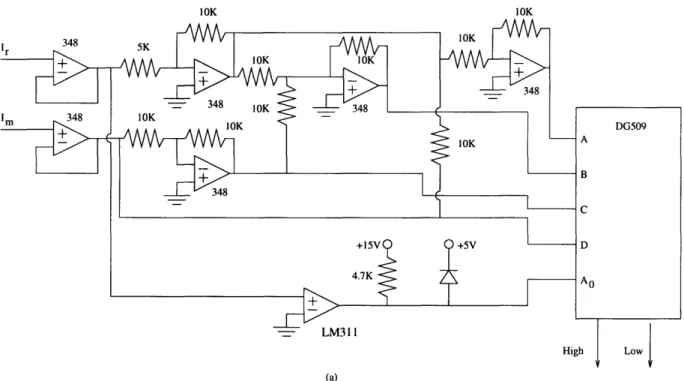
versions were experimented with. The final design is shown in Fig. 3-4. This design
implements an inexpensive and yet fully functional control system that may be used
at the elevated switching frequencies of the RPI.
The top circuit of Fig. 3-4(a) generates the appropriate hysteresis bands. The
inputs can be seen at the left hand side as I,. and I,,, and the outputs are shown at
the bottom of the DG509 as High and Low. The main component used in this part
of the control system is the LM348, a common op-amp. The 348's farthest to the
left are simply input buffers while the other ones are performing the additions and
subtractions required to obtain the desired hysteresis signals. Input A to the DG509
is then 21,-1, input B is 21,.+1m, input C is -Im, and input D is +I,.
The DG509 is a dual 4-channel analog multiplexer. It has 2 address inputs, Ao and
A
1, to control its dual 4 channels. Since the control system only needs to distinguish
between two states, namely when I, is positive or negative, only one address input is
required, in this case A
0. In order to select the appropriate state for Ao, a comparator
was introduced, the LM311. Whenever I, is larger than zero, the output of the LM311
is high, and whenever I, goes below zero, the LM311 output goes low. The conditions
for the High and the Low hysteresis bands are summarized in the Table 3.1.
The components selected for the circuit in Fig. 3-4(a) are all inexpensive but
also comparatively slow. This is, however, of little importance since this part of
the control system only generates the required hysteresis bands, which are based on
the relatively slow reference signal. The circuit in Fig. 3-4(b) deals with the fast
switching waveforms (possibly over 100kHz), so it is of vital importance that the
components in that part of the system are very fast. Fig. 3-4(b) shows that there are
only two different IC's in this part of the control system: a comparator (PM219) and
a flip-flop with set and reset (14027B). The PM219 is a very fast comparator with a
response time of only 80ns and an input offset voltage of only 0.7mV. The flip-flop is
not a particularly fast part: it has a set-to-Q response time of 150ns and a reset-to-Q
+15V4 PM219 PM219 + I5V
+5V
+5V
,L-- + 14027B RFigure 3-4: Schematic for the control system
'k RHighi k High To Gate Drive
I
+
+15V
"V
LAJW LowMresponse time of 350ns. The flip-flop was therefore replaced by its TTL functional equivalent, the LS279, in an updated version of the control system. The LS279 has a set-to-Q and a reset-to-Q response time on the order of 25ns. The experiments described in this chapter, however, are based on the system containing the 14027B.
There are three different inputs to the comparators: the current fedback from the inverter, Ik, and the High and Low signals. The fedback current is compared to the hysteresis bands, and if Ik is larger than High or smaller than Low the flip-flop changes its output state. It is worth noting the function of the resistor RIk: it scales the fedback current to an appropriate voltage level. It is evident that by changing the value of RIk, the magnitude of the inverter output current can be altered.
One drawback in using the fast PM219 comparator is that its maximum input voltage differential may not exceed 5V. Several attempted clamping schemes turned out to be unsuccessful, and it is therefore up to the designer to ensure that the input voltage differential limit is not exceeded for a specified value of RIk.
3.3
The Set-up for Testing the Control System
In order to be able to experiment with the control system, and to improve its char-acteristics, a complete converter system had to be assembled. The inverter cells used for this purpose had been designed by David Perreault and David Otten in LEES at MIT. A complete description of the inverter cells is included in appendix A.
Once the inverter cells had been constructed, some additional components also had to be designed and assembled. When connecting two or more inverter cells to each other, it is important to connect them through inductors, interphase transform-ers, or some other magnetic structure to provide buffering among the cell outputs. This buffering also enables control of current sharing among the cells. In this case, individual inductors were constructed using the method outlined in [12, pp. 575-77]. It was also decided to keep the power processed to a minimum for experimental rea-sons, and the bus voltage was set to a mere 25 V. The complete test set-up and its parameters are shown in Fig. 3-5.
V
dc/2V
doI2 c = 36 uF V = 25V dc R 1 2 Ohm L 7uHFigure 3-5: Test Set-up for developing the control system
3.4
Testing the Control System
Several tests were performed in order to demonstrate the functionality of the system.
First, only the control system was turned on, without applying any power to the
inverter bus. This was done in order to check that the control system generates the
appropriate hysteresis bands. All the oscilloscope pictures shown below were captured
by a black and white polaroid oscilloscope camera, and then scanned into a file by
means of a HP Scan-Jet IIc. The file was imported into the graphics package XV,
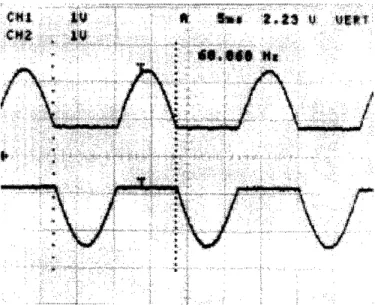
where it was inverted as well as digitally enhanced. Fig. 3-6 shows the two outputs
High and Low of the DG509. Here, I, is a 60Hz sinusoidal input, with a peak-to-peak
voltage of 1.6V, and I1,m is 0.8V. The input resistor in Fig. 3-4 has been set so that
the demanded current will be of the same magnitude as four times the magnitude of
Ir.
The voltage across the bus was then applied, and the system was allowed to run. In
order to verify that the control system was switching the inverters at the appropriate
CHI LV I~v U SJL?.
Figure 3-6: the DG509
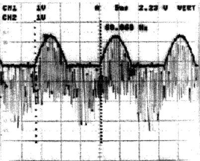
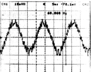
instances, and not letting the current signals exceed the desired hysteresis bands, another oscilloscope measurement was taken. A probe was attached to the High signal coming out of the DG509, and another probe was attached to measure the voltage across ik, due to the fedback current. Fig. 3-7 displays the result. The solid waveform shows the High signal coming out of the DG509, while the switching waveform is the fedback current. Fig. 3-7 seems to suggest that the control system is not functioning properly. In particular, the fedback current does not seem to always reach the upper hysteresis band before it starts falling again. As it turns out, this is not an error in the control system, but rather due to the sampling limitation of the oscilloscope. One way to demonstrate this fact is to look at the switching waveform at a smaller time scale. This is shown in Fig. 3-8. Not only does Fig. 3-8 show that the control system is working properly. It also shows that there is very little overshoot over the desired hysteresis band.
Another way to verify the functionality of the control system is by looking at the output currents. Instead of looking at the current fed back by the Hall-effect sensor, a current probe was attached just before the load resistor (R1 in Fig. 3-5).
... .
NOW,
Figure 3-7: The solid waveform shows the High signal (the upper hysteresis limit) coming out of the DG509, while the switching waveform is the fedback current
..
.
..
...
*
:: ·.:X's
.
..
.
.
..
.
.
.
.
.
.
Figure 3-8: Demonstration that the current switches at the upper ary. The solid waveform shows the High signal coming out of the switching waveform is the fedback current.
hysteresis bound-DG509, while the ;·i8i~·wu~u~·lu-ll~i~L~u~ ::: ii: :i
Figure 3-9: Output waveform as measured by a current probe attached just before
the load resistor R
1in Fig. 3-5. The scale is 2A/div.
Since only one inverter was run for this part of the experiment, the output waveform
measured by the current probe was not expected to be very clean since no harmonic
cancellation is present. A picture of the output current as seen on the oscilloscope
is shown in Fig. 3-9. The picture suggests that the control system is producing the
desired output waveform, even though there are plenty of harmonics. This is not
surprising, however, since only one inverter is operating. The peak-to-peak current
is about 6.4A, and the frequency is almost exactly 60Hz, which is precisely what was
expected.
Three inverter cells were then connected in parallel. Each cell was controlled by
its own independent control system. The three cells did, however, all have the same
input reference waveform, I,. Again, I, was set to be a 60Hz sinusoid with a
peak-to-peak voltage of 1.6V. The total expected peak-peak-to-peak output current would then
be 19.2A. The current probe was attached right after the joining node of the output
inductors (see Fig. 3-5), and was set to measure 5A per division on the oscilloscope.
The result of the current probe measurement is shown in Fig. 3-10. It is clear that the
total output current is marginally smaller than the expected peak-to-peak value of
19.2A. Here, the effects of harmonic cancellation are apparent: The output inductor
it~j
Figure 3-10: Three inverter cell output waveform as measured by a current probe attached right after the joining node of the output inductors in Fig. 3-5. The scale is 5A/div.
current from three inverters operating in parallel has very small ripple in comparison to the one inverter output, significantly reducing rms current ripple strain on the filter capacitor.
Finally, two more measurements were made to fully verify the system set-up. First, the current probe was attached to measure the current going into the filter capacitor,
Cf. The result is shown in Fig. 3-11. From Fig. 3-11 it is clear that the maximum ripple is about 3A, and the average ripple is less than 1A.
The last measurement in these series of experiments was made by attaching the current probe to the input of the load resistor. Since most of the ripple components have been filtered out by the filter capacitor, it is expected that the current going into the load should very much resemble the desired output current waveform I,. The result displayed in Fig. 3-12 shows that this indeed is the case. It is also interesting to note that the distortion on the waveform is significantly less than in the one inverter cell case (compare to Fig. 3-9). This is expected'due to the harmonic cancellation that occurs in a parallel inverter cell structure.
.
.
.
.
.
.
.
Figure 3-11: The current going into the filter capacitor for ating in parallel. The scale is set to 2A/div.
three inverter cells
oper-U
.
Figure 3-12: Output waveform as measured by a current probe attached just before the load resistor R1. The scale is set to 5A/div.
fact that a functioning control system for a parallel resonant pole inverter architecture has been successfully constructed. The attention can now be turned to setting up a complete PRPI system, which is the topic of the next chapter.
Chapter 4
The RPI System
4.1
Introduction
This chapter describes the resonant pole inverter system. The system in its entirety includes the RPI itself, the control system, the output inductor, the load, and the power supply. The specifications for the RPI are summarized in Table 4.1.
4.2
The Power Supply
The 300V dc power supply was implemented by rectifying a three-phase 208V input. This was achieved by attaching a variac and a three-phase diode bridge to the input from the mains. Beyond the fundamental three-phase bridge, some additional safety features were incorporated into the design. A schematic of the power supply is shown in Fig. 4-1.
As can be seen in Fig. 4-1 the path between the mains and the variac is interrupted by a heavy duty vacuum breaker in order to allow the user to shut down the system at
Bus Voltage Vb ,
300V
Peak Current Ipeak 44A
Switching Frequency f,, 20-80kHz
V
bus
Figure 4-1: Schematic of power supply
any instant. The output of the breaker is connected to the input of the three-phase variac which scales the ac input voltage appropriately. The output of the variac is subsequently connected to the diode bridge. The three-phase diode bridge was purchased as a package (Powerex ME501206) and is mounted on an appropriately sized heatsink.
4.2.1
Sizing the Capacitor
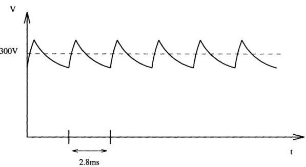
The role of the bus capacitor, CW, in Fig. 4-1, is to hold the output voltage steady at 300V. It needs to be large enough such that the bus voltage does not fluctuate significantly when the inverter is processing full current.
The capacitor is charged through the six-pulse rectifier. An illustration of how the capacitor voltage varies over time is shown in Fig. 4-2. In order to simplify the analysis, it is assumed that the capacitor is recharged to its full voltage by six impulses during each cycle. It is possible to solve for the capacitor value needed to
300V
I
I
t
2.8ms
Figure 4-2: Illustration of the variations in bus capacitor voltage over time
limit the ripple to a desired value by applying the following equation:
IA t
C =A
A V
(4.1)
Here, C is the bus capacitor value, At is the time between two pulses from the
rectifier, AV is the maximum voltage deviation allowed from the desired 300V in the
bus voltage, and I is the average current drawn by the inverter. Since Irma of the
inverter is specified to be 15A, the maximum current the inverter would ever draw
would be approximately 20A. If the bus voltage is allowed to fluctuate by 10% around
the 300V specified, the calculated bus capacitor value comes out to be approximately
10001tF. The value of the bus capacitor in the actual system was chosen to be 1600
11F,
simply because that particular value capacitor happened to be available.
It is worth noting that by increasing the capacitance of the bus capacitor, the
voltage bus will deviate less from the desired 300V. The disadvantages in making the
bus capacitor too large, however, are that it increases the stresses on the three-phase
diode bridge, and it makes it more difficult to discharge the capacitor when the system
is shut down.
4.2.2
Sizing the Resistors
The resistors are added for safety reasons only. They are included in the design so
that the energy stored in the capacitor can be dissipated safely. The resistor Raman
is the fastest means for dissipating the energy stored in the capacitor. By throwing
the switch to connect the small resistor in parallel with the capacitor, the capacitor
will discharge very quickly through Rmall. The discharge time was set to be less
than one second. This means that five times the RC time constant, r, must be less
than one second. In order to satisfy this condition, a resistor value of less than 125fI
is required. A suitable power resistor with a resistance of 9110 was available. It is
important to realize that this resistor must have a instantaneous current carrying
capacity of V,,, / R,malz=300/91=3.3A.
The resistor Rubi is needed to ensure that if the user turns off the variac but forgets
to discharge the energy stored in the capacitor manually through Rmait, the capacitor
energy will eventually discharge through Rbi, but over a longer time span. The upper
constraint on the resistance of Rbig is determined by the maximum allowable time to
fully discharge the bus capacitor. The lower limit is set by on-state power dissipation
limits, since Rbig dissipates power while the system is running. It was decided that
no more than 1W should be dissipated in
Rbig.
Then, from the equation,
Vs
Pdiss =
(4.2)
R
where V=Vb,, and R=Rbiu, it is clear that Rbig must be larger than 90kO. Picking
Rbig
to be 100k[ results in a discharge time of 5RbgCb, = 13 minutes.
4.2.3
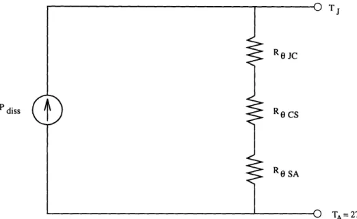
Sizing the Heatsink
As was mentioned above, the three-phase diode bridge was bolted to a heatsink.
The reason for this is that the losses in the bridge appear as heat, which then must
be removed from the system. The design of the heatsink is based on conservative
estimates as well as on information provided by the manufacturer.
RU JC
P
diss
Re
CS
RSA
T -27C'
'A=
Figure 4-3: The thermal system used for modeling the rectifier device, the device
casing, and the heat sink.
Idmax=6A0A Re.rc=0.3C/W
Recs=O.06'C/W VoN=1.3V
Table 4.2: Information about the rectifier available from the manufacturer
device, the device casing, and the heatsink as shown in Fig. 4-3 was used. Here,
TA represents the ambient temperature and
Tj
represents the junction temperature.
The three resistors model the thermal resistance between the junction and the case
(RoJc), between the case and the heatsink (Recs), and the heatsink and the ambient
temperature
(ROSA).
The information available from the manufacturer concerning
the three-phase diode bridge is summarized in table 4.2.3.
The information about the heatsink specifies that the thermal resistance between
the heatsink and the ambient is 0.350C/W. The only thing missing from the model is
then the value for Pdis, which is found by using the fact that two bridge diodes will
be conducting at any given time. From this:
SVbus
11
I-1_
I-Figure 4-4: Schematic of the RPI inverter
Assuming that the heatsink is sized to 6" results in a maximum junction
temper-ature of:
TJ = TA
+
Pdiss * (Resc+
Recs+
ReSA)TJ = 27 + 156 * (0.3 + 0.06 + 0.35)
(4.4)
Ti = 138°C
The three-phase rectifier device is rated to operate at 1500C, so this is clearly a
sufficient heatsink. While the inverter system will never process 60A, the heat sink
has been overrated to match the limits of the rectifier devices for future applications.
4.3
The Inverter
The inverter was designed in conjunction with David Perreault at LEES, MIT. A
schematic of the RPI is shown in Fig. 4-4. The power devices used in the RPI are
IXYS IXGH24N60AU1 IGBT's with internal diodes. In parallel with each IGBT is
the CD30FD103JO3 silvered mica resonant capacitor from Cornell Dubilier. The gate
signals for the IGBT's are provided by an IR2110 high voltage mos gate drive. The
low side channel (LO) is referenced to ground and the high side (HO) is referenced
to a floating rail Vs. The charging of the top capacitor is achieved by means of a
bootstrap technique, implemented by a resistor and a fast recovery diode BYV26C.
The conditions determining which switch is turned on are set by the control system,
the zero voltage detection system, and a startup signal. The startup signal is a simple
RC-network shorted by a switch. The startup signal starts at +5V, and the IR2110
will not receive HIN/LIN unless the startup signal goes low (achieved by throwing the
switch). The HISET signal is provided by the output of the control system. LOSET
is simply HISET inverted. Finally, the zero voltage detection signals for the low and
high side are provided by the zero voltage detection scheme outlined below.
During normal operation the startup signal will remain off. Assuming that the
bottom device is conducting, the output current will be decreasing. When the output
current reaches the level set by the control system, the control system will tell the
RPI to turn off the bottom switch and turn on the top switch by setting LOSET low
and HISET high. The RPI will turn off the bottom switch, but the top switch will
remain off. The bridge output node will then ring from zero to
Vb~.
When the top
device voltage reaches zero, the zero voltage signal for the high side will go low, and
the top switch will turn on. The same logic is used for top to bottom transitions.
4.3.1
Zero Voltage Detection
The zero voltage detection system detects whenever there is zero voltage across a
device. This information is required by the RPI in order to ensure zero voltage
turn-on/off. It is also used to detect zero current in some of the current sensing schemes
described in chapter 5.
The zero voltage detection schematic for the high side device is shown in Fig. 4-5.
It is implemented using a MAX913 comparator and a HCPL2611 opto-coupler. The
MAX913 and the input side of the opto-coupler are referenced with respect to the
V,
pin on the IR2110, while the output side of the opto-coupler is referenced to ground.
The positive input to the MAX913 is kept constant at 2.5V. Whenever the power
diode is conducting, the negative input to the MAX913 goes low, and the output (Q)
of the MAX913 goes high. The negative input could potentially go below zero, which
+5H +5H
Figure 4-5: Schematic of the zero voltage detection system.
is outside the operating region of the MAX913. The zener diode 1N749A prevents
this from happening by clamping the negative input at 0.7V. When the IGBT is
conducting, the negative input will go to at least 3.4V (2.6V from the IGBT, and
0.8V from the BYV26C). This will make the MAX913 output
(Q)
go high. The
HCPL2611 provides the required isolation, and also inverts the signal. Subsequently,
the zero voltage sensing system's output will be low whenever the power diode is
conducting, and will otherwise remain high.
The low side zero voltage detection scheme does not require the opto-coupler, but
in order to simplify debugging, it was constructed in the same manner as the high
side system.
4.4
The Load
The RPI was assembled in its entirety as shown in Fig. 2-1. A 30LH output inductor
was constructed by winding 21 turns on the Arnold Engineering core A-123068-2.
The load was a 2f power resistor, in parallel with a 36
1zF filter capacitor.
4.5
Testing the RPI
The RPI was successfully tested at low power levels. However, since neither the
control system nor the current sensing systems require an RPI during the design and
evaluation process, the RPI was not used to test either the control system or the
current sensing schemes.
Chapter 5
Current Sensing
5.1
Introduction
There are many different methods available to sense currents. Based on the cur-rent levels to be sensed in the system, and the cost and performance constraints, five different current sensing schemes have been selected as promising for this par-ticular application. Sensing current by resistive methods, by current transformer, by Rogowski coil, by Hall-effect, and via a secondary winding on the output induc-tor are considered. These schemes are evaluated with respect to three fundamental characteristics: Their accuracy, their bandwidth and their total cost.
5.2
The Hall Effect Sensor
5.2.1
Introduction
Out of the five different schemes that are being evaluated here, the Hall effect sensor is the most commercially available. It is also very accurate: The LEM50-A from LEM USA measures currents of up to 70A with an accuracy of 0.5% of full scale and can follow waveforms up to 100A/ts. Furthermore, it is also simple, non-intrusive, small, requires no additional circuitry and has a high bandwidth (0-150kHz). Unfortunately, it is also very expensive. Therefore, the Hall-effect sensor will be used primarily as a
Figure 5-1: The Hall effect sensor.
reference, and its performance will serve as a benchmark for the other current sensing schemes.
The Hall-effect sensor is built around a phenomena discovered by Edwin H. Hall in 1879. He showed that it is possible to deflect conduction electrons traveling in a conductor by means of a magnetic field. Consider a strip of silicon with a known level of doping. If a current is sent through the silicon while applying a magnetic field Bappi transverse to the direction V,e the electrons are traveling, the electrons will experience a deflecting force inside the conductor, as illustrated in Fig. 5-1. The magnetic deflection force, denoted as Fb in Fig. 5-1, pushes the electrons to the bottom of the strip, leaving uncompensated positive charges on the top edge. Therefore, a constant electric field will build up at all points inside the silicon strip, which acts on the electrons in the opposite direction from the magnetic force. An equilibrium will eventually develop where the magnetic force is exactly offset by the electric force, and the charge carriers will no longer be deflected. At this equilibrium, there will be a constant potential between the top and bottom of the silicon strip,
p
/
+
Lr Rload
V bus
[i
O
Figure 5-2: The setup for testing the current sensing systems.
called the Hall potential difference. This potential can be used to deduce the current going through the silicon strip as the current and the Hall potential difference are related through the following equation:
VHall te
I = (5.1)
Bapp,
Here, VHal denotes the Hall potential difference, t is the thickness of the strip, and e is the charge of an electron [13]. The equilibrium is established very rapidly, which makes this method very suitable for current measurements at elevated frequencies.
5.2.2
Testing the Hall-Effect Sensor
The five different current sensing methods were all tested under similar conditions. The test setup consisted of two inverter legs connected in an H-bridge as shown in Fig. 5-2. The specifications for the inverter cells are outlined in Appendix A. The control system was set up to generate dc-level hysteresis bands at 3 1,m and -Im by
simply connecting I, to the I, pin. This results in an output current waveform whose frequency and magnitude can be altered by changing I,, (implemented by means of
Figure 5-3: Output waveform for Hall-effect sensor (top waveform) as compared to a current probe measurement (bottom waveform). The setting is 2A/div, and the switching frequency 85.5kHz.
a 1KQ pot between +5V and ground). It also has the advantage that the magnitude and frequency stays fixed, unlike the RPI output waveform.
The Hall-effect sensor was tested at high and low current levels, as well as at high and low frequencies. First, the general output waveform of the Hall-effect sensor was examined. The switching frequency was set to about 85kHz in order to test high frequency behavior. The resulting oscilloscope picture is shown in Fig. 5-3. It is clear that the Hall-effect sensor measures current accurately even at the elevated frequency of 85kHz. In order to measure just how accurate the Hall-effect sensor is, two more measurements were made: One at low current levels, and one at high current levels. Figure 5-4 shows a measurement made at 1A/div and 60kHz. There are actually two traces superimposed which is evident if one examines the tip of the switching waveform: The waveform put out by the Hall-effect sensor contains some switching noise at the peak, while the current probe measurement is clean. Figure 5-4 shows that the Hall-effect sensor provides a very accurate current measurement at this current level and switching frequency. In fact, it is so accurate that any errors are difficult to discern. However, an error of approximately 0.5% can be seen in the
Figure 5-4: Output waveform for Hall-effect sensor (contains some switching noise) as compared to a current probe measurement (clean) at a high switching frequency. The setting is 1A/div and the switching frequency is 60kHz.
last measurement. The same turned out to be true for high current levels (and low switching frequency). Figure 5-5 shows the same measurement as in Fig. 5-4 except that now the switching frequency is only 13.3 kHz, and the oscilloscope is set to display 5A/div. The peak current can be seen to be about 30A.
5.2.3
Conclusion
On the basis of the measurements presented above, it is clear that the Hall-effect sensor possesses the required bandwidth and accuracy required for the control of an RPI. It is also small, and requires no additional components. The only disadvantage is the cost. The Hall-effect sensors used in these experiments cost about $34 each ($25 if bought in bulk), which is too expensive if the PRPI system is to become economically feasible. A summary of the findings for the Hall-effect sensor is shown in Table 5.1. The worst case error is the specified error from the manufacturer added to the 1% error from the resistor value. The measured error is the maximum approximate error found during the experiments documented above. The cost and the bandwidth were specified by the manufacturer.