HAL Id: hal-01887159
https://hal.archives-ouvertes.fr/hal-01887159
Submitted on 15 Oct 2018
HAL is a multi-disciplinary open access
archive for the deposit and dissemination of
sci-entific research documents, whether they are
pub-lished or not. The documents may come from
teaching and research institutions in France or
abroad, or from public or private research centers.
L’archive ouverte pluridisciplinaire HAL, est
destinée au dépôt et à la diffusion de documents
scientifiques de niveau recherche, publiés ou non,
émanant des établissements d’enseignement et de
recherche français ou étrangers, des laboratoires
publics ou privés.
Power Efficiency and EMI Attenuation Optimization in
Filter Design
Moises Ferber, Roberto Mrad, Florent Morel, Gaël Pillonnet, Christian
Vollaire, Angelo Nagari
To cite this version:
Moises Ferber, Roberto Mrad, Florent Morel, Gaël Pillonnet, Christian Vollaire, et al.. Power
Ef-ficiency and EMI Attenuation Optimization in Filter Design. IEEE Transactions on
Electromag-netic Compatibility, Institute of Electrical and Electronics Engineers, 2018, 60 (6), pp.1811 - 1818.
�10.1109/TEMC.2017.2765921�. �hal-01887159�
Power Efficiency and EMI Attenuation
Optimization in Filter Design
Moises Ferber, Roberto Mrad, Florent Morel, Senior Member, IEEE, Ga¨el Pillonnet, Member, IEEE,
Christian Vollaire, Member, IEEE and Angelo Nagari, Senior Member, IEEE
Abstract—This paper presents a discrete conducted electro-magnetic interference filter optimization procedure, based on a Genetic Algorithms. A macro-modeling technique taking into account the load impedance, the source emissions and the filter parasitic components, including the filter layout, is used to obtain an accurate solution for the optimization process. The latter searches among supplier passive component databases and provides, for a given filter topology, an optimal set of components available on the market. This approach has been applied to a differential Class-D audio amplifier for validation. By considering the EMI, the additional power losses introduced by the filter and the audio gain, two different optimization formulations have been tested. The first corresponds to maximizing the power efficiency of the system while respecting a determined level of electromagnetic emissions. The second corresponds to minimizing the EMI without exceeding a determined level of power loss. The optimized filters are built and measurements are carried out. The results show a remarkable power efficiency improvement and a significant EM emission reduction when compared to a reference filter.
Index Terms—Conducted immunity and emissions, Filtering, Passive component modeling and measurement techniques, Power electronics, Printed circuit board EMC.
I. INTRODUCTION
Nowadays, electronic devices demand high power due to the diversity of applications in the same device. Switching power converters and power management circuits are therefore widely used. Generally, such circuits have high electromag-netic (EM) emissions, because they deal with switching signals and they provide higher power, compared to their surrounding electronics. To avoid any system dysfunction, electromagnetic interference (EMI) filters are used in most cases. A filter’s performance is measured by its high frequency insertion loss. Therefore, stray elements have a direct impact on the filter’s effectiveness [1]. Moreover, EMI filters are in the electrical power path and if they are not adequately designed, they can lead to high power losses due to parasitic resistances. Thus, they can reduce the overall power efficiency.
To confirm this issue, power measurements on a low power Class-D amplifier for a hands-free mobile phone application have been made, with zero and low audio signal level (-20 dB full scale). At the supply pin, we recorded an average of 10 mW and 50 mW of power consumption when the amplifier is used without and with an EMI filter, respectively. Therefore, due to the EMI filter, the system consumes 5 times more at low output power. In [2], it has been shown that in a real audio signal (i.e. Jazz song), there are more amplitude levels lower than -20 dB full scale than the higher amplitudes for
a 10 s recording. Thus, it can be deduced that a Class-D amplifier runs most of the time at low signal levels. As a result, the additional power losses due to the EMI filter is a crucial parameter in filter design for battery-powered, audio applications.
Some electromagnetic compatibility experts rely on expe-rience to design EMI filters. Other designers refer to the classical filter design methodology, which consists in de-termining the required attenuation of conducted emissions relative to a given EMI standard or system specification, and then computing the values of inductances and capacitances analytically for a given topology [3]–[9]. These procedures may lead to sub-optimal solutions for EMC, volume, area and specially power efficiency. Thus, the filter design formulated as an optimization problem can be advantageous. Even though one can find many papers about EMI filter design, to the best knowledge of the authors, no work has investigated yet the problem of maximizing the power efficiency of an EMI filter, while keeping a determined level of EMI attenuation or maximizing EMI attenuation, while keeping a determined level of power efficiency.
A continuous optimization procedure has already been ap-plied to EMI filter design for power electronics [10], [11], for aerospace applications [12], [13] and for signal process-ing [14]. However, this type of optimization can be improved. Passive filters are constituted of standard components available on the market, such as surface mounted technology (SMT) components. These have discrete nominal values. Component nominal values given by a continuous optimization are most of the time unavailable from suppliers. Additionally, SMT component suppliers provide component libraries that take into account high frequency behavior. Therefore, optimizing a filter according to the available components on the market is much more realistic.
The number of available components on the market, con-sidering all suppliers, is very high. For instance, a filter of 5 components and 100 items per component, which is a fairly small problem, corresponds to a discrete design space of size (102)5 = 1010. Considering that each function evaluation
takes about 1 s, the time required for an exhaustive search would be more than three hundred years, thus, impractical. Discrete optimization methods are able to explore a very small subset of the design space and find the global optimal or a design which is near to the global optimal.
Previous work in filter optimization such as [15]–[19], neglect or give less importance to the parasitic effects of com-ponents and printed circuit board (PCB) tracks. Nevertheless,
this part is essential in high frequency EMI modeling. In [20], the equivalent series resistance, capacitance and inductance of passive components are modeled with lumped circuit el-ements as an attempt to increase accuracy in EMC analysis and optimization. However, there is no simple expression that links these parasitic effects to the component nominal value. Therefore, using the component models provided by the supplier is the most adequate choice.
In [21], the authors propose an automated filter design based on discrete optimization by Genetic Algorithms (GAs). The optimization runs on a sub-system level macro-modeling technique in the frequency domain which relies on impedance matrix manipulation. The approach is presented in [22], [23]. It allows the source emissions and the load impedance to be included for a fast and accurate electromagnetic emission computation. The filter, having a fixed topology [24], is implemented in Advanced System Design (ADS) software. Therefore, most of the filter imperfections such as the PCB layout and PCB stray components are taken into account. The filter components are replaced by their models provided by the suppliers in a library of models referring to their products. The GA searches among these components and generates an impedance matrix from the ADS filter model. Finally, based on the criterion calculated using the macro-model, the optimization process extracts a set of components corresponding to the optimal solution. Note that the component references are given and they can be found on the market.
The present paper extends [21], by giving more details about the optimization and testing two different problem formulations. The first formulation aims to maximize the filter power efficiency while respecting the EM emission limit. The second formulation aims to reduce the system EM emissions without decreasing the system power efficiency. Both formulations are solved numerically and validated with experimental measurements. Finally, a comparison between the two formulations is made to highlight the existing trade-off between power efficiency and EMC performance.
The remainder of this paper is organized as follows: in Section II, the problem formulation is presented. Then, in Section III, the modeling method, the power computation expressions and the optimization methodology are depicted. In Section IV, the application on a Class-D amplification system is presented. Section V presents the experimental results. Finally, in Section VI, a conclusion is presented.
II. PROBLEMFORMULATION
A simplified block diagram of a system composed of a source of EM emissions, an EMI filter and a load is pre-sented in Fig. 1 and will be used in the following problem formulations as optimization problems.
A. Formulation I: Power efficiency maximization
The first problem consists of maximizing the power effi-ciency of an arbitrary filter topology, such that a determined level of EMI attenuation is achieved and there is no significant impact on the audio signal caused by a voltage drop in the audio band. The decision variables in the input vector x are the
𝑍𝐹 𝑍𝐿
EMI Filter Load Class-D Amplifier 𝑉𝑆 𝐼𝐼𝑁1 𝑉𝐼𝑁1 𝐼𝐼𝑁2 𝐼𝑂𝑈𝑇1 𝐼𝑂𝑈𝑇2 𝑉𝐼𝑁2 𝑉𝑂𝑈𝑇1 𝑉𝑂𝑈𝑇2
Fig. 1. System block diagram.
component models available in the libraries of the suppliers. Thus, the entries of x are black-box models of resistors, inductors and capacitors, which are accurate up to at least 100 MHz.
The maximization of power efficiency can be formulated as a minimization of the system’s power losses, here denoted as PSY S. The constraints related to the EMI level and the
audio quality are implemented as penalty factors in the fitness function f (x), which is given by the following expression:
f (x) = PSY S+ PEM I+ PA (1)
where PEM I and PA are equivalent power losses penalty
associated with EMI level and audio quality, respectively. For instance, given a x, if the EMI attenuation is achieved, then PEM I = 0. Otherwise, PEM I is a high number relative to
PSY S. The same criterion is applied to PA.
Thus, the problem is formulated as: minimize
x f (x)
such that x ∈ L
(2) where L is the collection of components from all supplier libraries.
B. Formulation II: EMI attenuation maximization
The second problem consists of maximizing the EMI atten-uation of an arbitrary filter topology, such that a determined power efficiency is achieved, without impact on the audio sig-nal. The maximization of EMI attenuation can be formulated as a minimization of EMI level, after the filter is introduced, here denoted as EM ISY S. The EMI level EM ISY Sis defined
as:
EM ISY S =
X
|IINk,F(jω)|>|IINk,REF(jω)|
|IINk,F(jω) − IINk,REF(jω)|
+ X
|IOU Tk,F(jω)|>|IOU Tk,REF(jω)|
|IOU Tk,F(jω) − IOU Tk,REF(jω)|
such that ω ∈ Ω and k ∈ {1, 2},
(3) where IINk,F(jω) and IINk,REF(jω) are the input currents
with an arbitrary filter and the reference filter, respectively, and IOU Tk,F(jω) and IOU Tk,REF(jω) are the output currents with
an arbitrary filter and with the reference filter, respectively, ω is the angular frequency and Ω is the set of considered
frequencies. In other words, EM ISY S is the sum of the
differences between the module of the current spectrum peaks of a given filter and those of the reference filter when the peaks are lower then the ones of the reference filter.
If no reference filter exists, one may use IINk,DES and
IOU Tk,DES instead of IINk,REF and IOU Tk,REF, respectively,
where the subscript DES refers to a maximum desired value for the current flowing in the power path.
The constraints related to the power efficiency level and the audio quality are also implemented as penalty factors in the fitness function f (x), which is given by the following expression:
f (x) = EM ISY S+ EM Iη+ EM IA (4)
where EM Iηand EM IAare equivalent EMI penalties
associ-ated with power efficiency level and audio quality, respectively. For instance, given a x, if a determined power efficiency is achieved, then EM Iη = 0. Otherwise, EM Iη is a high
number relative to EM ISY S. The same criterion is applied
to EM IA. The penalties are applied if any current peak of
the given filter spectrum exceeds the one obtained with the reference filter.
Here, the problem formulation is identical to (2) with f (x) given by (4).
III. METHODOLOGY
The methodology developed in this paper is presented in three subsections as follows.
A. Modeling approach
A frequency-domain modeling approach presented in [22] was used. This method was chosen because it is a subsystem level macro-modeling technique. It can be easily applied on single phase systems such as DC-DC converters [25], differen-tial systems such as the integrated Class-D amplifiers [23] or even N-phase systems. This approach is particularly interesting for studying the filter in the final application, according to a specific EMI source and load with a good accuracy at high frequencies.
An accuracy limitation of this modeling approach is related to not taking into account the electric and magnetic coupling between components and between component and PCB tracks, which can be very important [26], [27]. However, this model has a short simulation time compared to the traditional tran-sient simulations, which is a great advantage when integrated in an optimization loop in EMI filter design.
The considered frequency modeling approach consists in decomposing the system into functional blocks, as shown in Fig. 1. Three blocks can be seen in this figure: the Class-D amplifier, the filter and the load. The Class-Class-D amplifier is modeled by electric sources and an impedance matrix that corresponds to the Class-D amplifier output impedance. The load is modeled by an impedance matrix if it is a passive load or by electric sources and an impedance matrix if it is an active load. The sources and impedance matrices of the Class-D amplifier and load can be measured or simulated. Finally, the
filter is modeled by an impedance matrix that can be obtained by a dedicated analytical model or an implemented model in a simulation software. The model of each filter component, if not given by the supplier, can be obtained by, an impedance measurement, a scattering parameter measurement, or by their equivalent analytical or fitting models. More details can be found in [22].
Many possibilities can be used to compute the filter impedance matrix. The filter high frequency behavior depends on the filter parasitic stray elements. In this work, the ADS software [28] is used to model the filter. The model includes the filter layout design and all the PCB physical characteristics. Thus, the stray elements related to the filter layout such as track impedance are taken into account. In this model, the components are black-box models provided by the suppliers. Hence, the passive component stray elements related to the technology and packaging of each component are taken into account. Finally, the ADS generates an impedance matrix including most of the filter stray elements and non-ideal impedance behavior for better accuracy at high frequencies.
B. Power computation
Using the model presented earlier, it is possible to compute voltages and currents at any system node. Hence, the power losses of a system (PSY S), composed of a Class-D amplifier,
filter and load losses are computed as follows: PSY S= PP S + PF L− PA
| {z }
filter and load losses
(5)
where PP S represents the losses in the power stage, PF L
represent the power delivered to the filter and the load, PA
is the power of the audio signal. They can be obtained by equations (6), (7) and (8), respectively.
PP S= RDSon(IIN2 1+ I
2
IN2) (6)
where RDSon is the power switch-on resistor, IIN1 and IIN2
are the RMS input currents of the filter, which are the same as the power stage output currents.
PF L= n X k=1 Real{VIN1(fk) · I ∗ IN1(fk)} + Real{VIN2(fk) · I ∗ IN2(fk)} (7)
where VIN1 and VIN2 are the filter input voltages and k is the
index of the frequency vector of size n. Note that PF L also
includes the power in the audio band. Therefore, PAmust be
computed and deduced from the total power loss PSY Sin (5).
PA= Real{[VOU T1(fA) − VOU T2(fA)] · I
∗
OU T1(fA)} (8)
where VOU T1(fA) and VOU T2(fA) are the filter output
volt-ages and IOU T1(fA) is the filter output current, all at the audio
frequency fA. Here, the considered audio signal is a pure sine
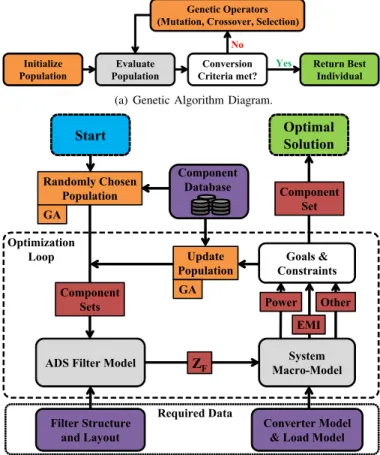
InitializeY Population Evaluate Population ReturnYBest Individual GeneticYOperators (Mutation,YCrossover,YSelection) ConversionY CriteriaYmet? Yes No
(a) Genetic Algorithm Diagram.
GoalsUq Constraints EMI Power Other RandomlyUChosenU Population SystemU Macro-Model ZF Update Population Component Database ADSUFilterUModel Optimal Solution GA GA Start FilterUStructureU andULayout ConverterUModel qULoadUModel RequiredUData Optimization Loop Component Sets Component Set
(b) Optimization by using the Genetic Algorithm. Fig. 2. Optimization methodology
C. Design by Optimization
The design of an EMI filter can be summarized by two main steps: (i) determine a filter topology, (ii) choose the components. Generally, the filter structure can be found by using common structures in the literature, or in some cases, a complex design can be made following the specifications of the application itself. Once the filter topology is decided upon, the choice of the components can be made by experience, by an analytical approach or by optimization, which is the method considered in this work.
Genetic Algorithms are an appropriate method for the problem considered in this paper, due to the following reasons:
• no initial point is available;
• the problem is discrete and multi-modal;
• there is no need for the fitness function to be analytical. The general diagram representing the optimization by GAs and the application to the present study are shown in Fig. 2(a) and Fig. 2(b), respectively. The initial population is generated randomly, over the input range. In the context of this paper, the input range is defined as the set of indices of the available components in the database of resistors, inductors and capac-itors. The population is then evaluated using a circuit analysis methodology. Here, the component set of each individual is transmitted to the ADS filter model where it generates an impedance matrix referring to an individual from the current population. When fed to the macro modeling, the impedance matrix allows a current and voltage spectrum computation
R L C 1 121 201 R L C 1 101 201 Mutation Crossover Individual 1 Individual 2 R L C 1 121 201 R L C 1 101 201 Individual 1 Individual 1 Individual 1 Individual 2 R L C 1 101 201 R L C 1 121 201
Fig. 3. Mutation and crossover examples.
directly in the frequency domain, as well as the attenuation of the signal at the audio frequency. Thus, the power consumption and EMI level can be computed.
The convergence criteria are then evaluated. A maximum number of generations is defined, based on the number of cores available for the computation and clock frequency of each core, and also a tolerance of the fitness function. For instance, if the EMI objective has not changed in the last generations, then this convergence criterion has been met. If all convergence criteria have not been met in the current generation, then the genetic operators are applied to update the population.
The mutation operator consists in changing an index of an arbitrary component. This usually happens with a low probability, which is defined by the user. For example, with a probability of 1%, an arbitrary inductor may be changed from a catalog reference Ref xxx1 to a Ref xxx2. Fig. 3 shows an example of mutation applied to a filter with 3 components to be optimized, in which the inductor was changed.
The crossover operator consists in considering two individ-uals, each having their components indices, and exchanging an arbitrary index between them, with a probability also defined by the user. For example, consider two filters having inductors of a catalog reference Ref xxx1 (Filter A) and Ref xxx2 (Filter B), respectively. If the crossover operator is applied, then Filter A has now an inductor reference Ref xxx2 instead of Ref xxx1. Similarly, Filter B has an inductor of reference Ref xxx1 instead of Ref xxx2. Fig. 3 shows an example of applying a crossover operator.
The selection operator consists in selecting the individuals with a probability based on the fitness evaluation. Thus, individuals with a better fitness have a higher probability of being selected to be part of the population in the next generation.
Finally, after several generations, the best individual of the current population is expected to be an improvement relative to the best individual of the initial population.
IV. APPLICATION
Embedded systems, such as cellphones, tablets and music players, are often used in everyday life. Reducing power consumption is a major challenge in order to increase the device autonomy. For audio applications, Class-D amplifiers present an interesting solution to increase the power efficiency. In general, the speaker and amplifier are far from each other
VIn VRamp VCM VOut VBat VBat VPWM-p VPWM-n + -+ + -+
-Fig. 4. Class-D amplifier differential architecture [29] without EMI filter.
due to their placement on the PCB. Therefore, as the Class-D amplifier is a switching circuit, an EMI filter is used to mitigate the flow of high frequency currents through the long PCB tracks that connect the amplifier to the loudspeaker. These currents may be the cause of radiated emission problems. Thus, this application is a good example for the validation of the proposed method.
In the next subsection we start by giving an overview of Class-D amplifiers. The filter architecture, the SMT compo-nent libraries and the load in use are then presented. Finally, the additional power losses introduced by the EMI filter are then exposed and their calculation is explained.
A. Class-D amplifier
A Class-D amplifier is a switching device composed of a switching power stage controlled by Pulse Width Modula-tion (PWM) [29]. Generally, in integrated soluModula-tions such as cell phones, differential architectures are used due to higher power delivery characteristics. The modulation is obtained by comparing the audio signal to a ramp at around a 400 kHz. Two alternating opposite width PWM signals are obtained (see Fig. 4), that control two switching cells which form the power stage. The latter feeds the speaker load by the amplified switched audio signal. Note that this type of amplifier, also called filterless Class-D amplifier, does not need a filter to reconstitute the audio signal due to the inductive nature of the micro-speakers [30] and because the switching harmonics are outside the audio frequency band. A filter is only needed for EMC reasons.
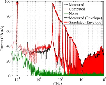
In this work, a test chip of a classical PWM differential Class-D amplifier is used. The amplifier output voltages have been measured for the same operating points in three different load conditions. The first is the operation with an open circuit, the second is the operation with a speaker load and the third is the operation with an EMI filter and a speaker load. Only two cases are shown in Fig. 5 for a clearer presentation of the results. The spectra are identical over the considered frequency band. Thus, it can be deduced that the amplifier voltage is independent of the load and the amplifier output impedance is negligible over the frequency range.
Fig. 5. Amplifier output voltage for two different load conditions.
Several simulations and measurements of the output volt-ages of the Class-D amplifier aforementioned were carried out. The worst-case scenario of audio signal considering EMI level is when the amplifier is operating with low input audio. Therefore, this scenario was used in the optimization. The Class-D amplifier output voltages considered are shown in Fig. 5.
B. Load
The load has been chosen as a dummy load that emulates the speaker. It is composed of an 8 Ω resistor and two 15 µH inductors mounted on a PCB. As a passive load, it can be modeled as an impedance matrix. Therefore, it has been measured using an impedance analyzer as explained in [22]. C. EMI filter and passive components
In [24], an EMI filter topology for Class-D amplifiers is presented, which is also shown in Fig. 6. It has been chosen as a reference filter to validate our optimization approach. This common and differential mode filter has nine components which include two inductors, two resistors and five capacitors. To ensure the symmetrical nature of the filter, thus, avoiding any differential to common mode conversion, and vice versa, some components must be identical. Hence, the problem consists of choosing the components L1, R1, C1, C3 and
C4, the five parameters to be optimized. The parameters R2,
L2, C2 and C5 are automatically chosen by symmetry. This
topology has been implemented in the ADS [31] software, for the optimization routine. The PCB tracks have been modeled as microstrip lines. The PCB characteristics have also been taken into account.
The libraries of SMT components have been chosen in the following manner: the inductors can be selected from TDK [32] and Murata [33] suppliers whereas the capacitors only from Murata. The resistors are chosen from a set of discrete values, since their impact on the results are much smaller than the other components. Thus, a database has been
L1 L2 C3 C2 C1 R1 R2 C4 C5 Vin2 Vin1 Vout2 Vout1 Iin1 Iin2 Iout1 Iout2
Fig. 6. Class-D EMI filter in use.
𝑳𝟏 𝑳𝟐 𝑪𝟑 𝑪𝟒 𝑪𝟓 𝑹𝟏 𝑹𝟐 𝑪𝟏 𝑪𝟐
Fig. 7. Filter layout.
created in MATLAB referring to these three libraries to be included in the optimization routine. Note that as the footprint of each filter component must be chosen for the layout, the capacitors have been defined as a 1005 (metric) SMT package and the inductors as a 7045 (metric) SMT package. In total, there are 718 capacitors, 8 inductors and 93 resistors in the database, with ranges of 0.1 pF to 10 µF, 1.5 µH to 22 µH and 1.0 Ω to 10 kΩ, respectively.
V. EXPERIMENTALRESULTS
The optimization routine based on Genetic Algorithms was executed in the MATLAB-ADS framework. The computer used is an Intel Quad Core i7 2.50 GHz with 16 GB of RAM memory. The entire optimization process required 3 hours, 5 minutes and 7 seconds for the power efficiency case and 3 hours, 5 minutes and 26 seconds for the EMI attenuation case. There is no reason to explain the differences between these optimization processes except variable computer back-ground processes. The reference filter as well as the optimized filters according to power efficiency and EMI attenuation are presented in Table I.
Prototypes for all filters shown in Table I have been built and used in the measurement validation. The filter layout is the same for all the filters and is shown in Fig. 7. The measurement bench with the prototypes (see Fig. 8) has been placed in an anechoic chamber to reduce the ambient EM noise. The input currents, output voltages and output currents are measured with a current probe [34] and voltage probe connected to a high resolution oscilloscope [35]. The measurement probes have an impact on the spectra results, since they add parasitic stray components when connected to the circuit. Therefore, the parasitic effect of the probes were taken into account when comparing simulation and measurement results.
In Fig. 9, it is shown a comparison between measured and simulated input currents for the reference filter, in order to
Fig. 8. Hardware for experimental results.
Fig. 9. Filter input current.
validate the accuracy of the modeling approach. The input current is chosen, as it has a higher spectrum level than the measurement noise floor. Thus, it is possible to make a good comparison over the entire frequency range. In Fig. 9, it is shown that the measured and the simulated input currents are in good agreement well up to 100 MHz, which is the measurement setup accuracy and model validity limit.
The output currents of the optimized filters are very low, in fact lower than the measurement noise floor. Therefore, the measured output voltages are shown for comparison. In Fig. 10, it is shown the envelopes of the output voltages, which are the voltages on the load, in the following cases: (1) no filter is used, (2) the reference filter is used and (3) the power efficiency optimized filter is used (formulation I) and finally, (4) the EMI attenuation optimized filter (formulation II) is used.
It can be seen that no significant variations occur in the au-dio signal level at 10 kHz which is due to the auau-dio constraint in the objective functions. In addition, the spectrum peaks are higher when there is no EMI filter. A considerable emission reduction can be observed when introducing any filter. In particular, the optimized filters offer a significant reduction in the spectrum compared to the reference filter, specially at around 400 kHz. The output spectrum has approximately 20 dB of additional reduction compared to the reference filter. Between 5 MHz and 50 MHz, the voltage level is lower than the measurement noise floor, and so no comparison is possible. Beyond 50 MHz, the reference filter has a better EMI behavior.
TABLE I FILTER COMPONENT VALUES
Reference Filter [24] Power Efficiency Optimized EMI Attenuation Optimized
Component Value Reference Code Value Reference Code Value Reference Code
L1, L2 15 µH CLF 7045T − 150M 22 µH CLF 7045T − 220M 22 µH CLF 7045T − 220M
C1, C2 0.033 µF GRM 155R71C333KA01 0.74 µF GRM 155R60J 474KE19 0.1 µF GRM 155R61H104KE19 C4, C5 0.068 µF GRM 155R61A683KA01 1.2 pF GRM 1535C1H1R2CDD5 0.1 µF GRM 155R61H104KE19
C3 0.15 µF GRM 155R61A154KE19 0.1 µF GRM 155R61H104KE19 0.47 µF LLL153C70G474M E17 R1, R2 22 Ω CP F 0402B22RE1 1.6 Ω M C0.0625W 04021%1R60 1.3 Ω M C0.0625W 04021%1R30 104 105 106 107 108 30 40 50 60 70 80 90 100 110 120 130 FCHz) dB µ V NofFilterfCEnvelope) ReferencefFilterfCEnveloppe) PowfLossfOptfCEnvelope) EMCfOptfCEnvelope) NoisefCEnvelope)
Fig. 10. Measurement comparison of filter’s output voltage envelopes.
This can be expected as the optimization process does not consider this frequency band in the EMI criterion. Finally, it can been seen that both of the optimized filters have a similar filtering effect. This can be explained by the fact that, with the considered component database, it is not possible to obtain better results.
In Fig. 11, it is plotted a percentage comparison for the additional power losses introduced by each filter, relative to the audio output power. The additional power losses percentage (PADD) is calculated using (9)
PADD= 100 ∗
PSY S− PSY S−N F
PSY S−N F
(9) where PSY Sis the power consumption measured at the supply
pin when using an EMI filter and PSY S−N F is that measured
at the supply pin when no filter is used.
As it can be seen in Fig. 11, the reference filter can introduce up to 500 % of additional power losses at low audio signal level when compared to the EMI attenuation optimized filter, and 520 % when compared to the power efficiency optimized filter. Thus, the optimization routine was effective in designing a much better filter than a classical methodology. Moreover, the power efficiency formulation proposed a filter more efficient than the EMI attenuation formulation. This result is in agreement to the theory.
It can also be deduced, from Fig. 11, that an EMI filter adds less power dissipation at high audio output power. This
0.1 1 10 100 1000 0.00 0.01 0.10 1.00 Ad dit ional Pow er Los ses (% )
Audio Output Power (W)
Reference Filter Pow Loss Optimized EMC Optimized
500 %
40 %
Fig. 11. Power losses introduced by the different EMI filters.
can be explained by the fact that at a high output power, which corresponds to a high differential audio signal level, the output currents have less common mode. In consequence, the common mode capacitors contribute less to the total power losses.
VI. CONCLUSION
A new perspective in EMI filter design, which is the reduction of power efficiency after a filter is introduced to a system, has been presented and discussed. It was shown that the impact of an EMI filter on power efficiency is significant and, therefore, it should be taken into account in design methodologies.
In this context, two optimization formulations for EMI filter design that consider power efficiency have been presented. The first formulation focus on maximizing power efficiency given a desired EMI level whereas the second formulation focus on maximizing EMI attenuation given a desired power efficiency. Both formulations address the considered problem, but each give emphasis on different requirements.
In addition, the proposed methods utilize components from libraries of suppliers instead of unrealistic values. The main advantage of this approach is that the result of the optimization routine is a list of components, which can be directly ordered from the suppliers. This is a very convenient characteristic of a filter design method.
The methodologies were presented in detail and the results were validated experimentally. Both formulations proposed
filters with higher inductances and capacitances (except the differential capacitor) but with lower resistances. The proposed method designed filters with at least 500% power losses reduc-tion and 20 dB addireduc-tional EMI attenuareduc-tion when compared to a reference filter, which shows the effectiveness and relevance of this work.
REFERENCES
[1] R. L. Ozenbaugh and T. M. Pullen, EMI Filter Design, third edition ed., 2011.
[2] P. Russo, F. Yengui, G. Pillonnet, S. Taupin, and N. Abouchi, “Dynamic voltage scaling for series hybrid amplifiers,” Microelectronics Journal, vol. 44, no. 9, pp. 753 – 763, 2013. [Online]. Available: http://www.sciencedirect.com/science/article/pii/S0026269213000864 [3] C. Jettanasen and A. Ngaopitakkul, “Reduction of Common-Mode
Con-ducted Noise Emissions in PWM Inverter-fed AC Motor Drive Systems using Optimized Passive EMI Filter,” in American Institute of Physics Conference Series, ser. American Institute of Physics Conference Series, vol. 1285, Oct. 2010, pp. 450–460.
[4] J. Kotny, T. Duquesne, and N. Idir, “EMI Filter design using high frequency models of the passive components,” in Signal Propagation on Interconnects (SPI), 2011 15th IEEE Workshop on, may 2011, pp. 143 –146.
[5] F. Viani, F. Robol, M. Salucci, and R. Azaro, “Automatic EMI filter design through particle swarm optimization,” IEEE Transactions on Electromagnetic Compatibility, vol. 59, no. 4, pp. 1079–1094, Aug 2017. [6] X. C. Wang, Y. Y. Sun, J. H. Zhu, Y. H. Lou, and W. Z. Lu, “Folded feedthrough multilayer ceramic capacitor EMI filter,” IEEE Transactions on Electromagnetic Compatibility, vol. 59, no. 3, pp. 996–999, June 2017.
[7] D. Shin, S. Kim, G. Jeong, J. Park, J. Park, K. J. Han, and J. Kim, “Analysis and design guide of active EMI filter in a compact package for reduction of common-mode conducted emissions,” IEEE Transactions on Electromagnetic Compatibility, vol. 57, no. 4, pp. 660–671, Aug 2015.
[8] V. Tarateeraseth, “EMI filter design: Part iii: Selection of filter topology for optimal performance,” IEEE Electromagnetic Compatibility Maga-zine, vol. 1, no. 2, pp. 60–73, Second 2012.
[9] H. Chen, P. Meng, J. Li, and Z. Qian, “Series-connected grounding of common-mode EMI filter,” IEEE Transactions on Electromagnetic Compatibility, vol. 52, no. 4, pp. 1066–1068, Nov 2010.
[10] L. Gerbaud, B. Toure, J.-L. Schanen, and J.-P. Carayon, “Modelling pro-cess and optimization of EMC filters for power electronics applications,” COMPEL: The International Journal for Computation and Mathematics in Electrical and Electronic Engineering, vol. 31, no. 3, pp. 747 – 763, 2012.
[11] Y. Poire, O. Maurice, M. Ramdani, M. Drissi, and A. Sauvage, “SMPS Tools for EMI Filter Optimization,” in Electromagnetic Compatibility, 2007. EMC Zurich 2007. 18th International Zurich Symposium on, sept. 2007, pp. 505 –508.
[12] A. Griffo and J. Wang, “Design optimization of passive DC filters for aerospace applications,” in Power Electronics, Machines and Drives (PEMD 2010), 5th IET International Conference on, april 2010, pp. 1 –6.
[13] F. Barruel, J. Schanen, and N. Retiere, “Volumetric optimization of passive filter for power electronics input stage in the more electrical aircraft,” in Power Electronics Specialists Conference, 2004. PESC 04. 2004 IEEE 35th Annual, vol. 1, june 2004, pp. 433 – 438 Vol.1. [14] S. Dhabal and P. Venkateswaran, “An Efficient Nonuniform Cosine
Modulated Filter Bank Design Using Simulated Annealing,” Journal of Signal and Information Processing, vol. 3, no. 3, pp. 330 –338, 2012.
[15] M. Caponet, F. Profumo, and A. Tenconi, “EMI filters design for power electronics,” in Power Electronics Specialists Conference, 2002. pesc 02. 2002 IEEE 33rd Annual, vol. 4, 2002, pp. 2027 – 2032.
[16] J. Le Bunetel, D. Gonzalez, A. Arias, and J. Gago, “A case study of design improvement based on EMI simulation,” in Compatibility in Power Electronics, 2007. CPE ’07, 29 2007-june 1 2007, pp. 1 –4. [17] S. Busquets-Monge, J.-C. Crebier, S. Ragon, E. Hertz, D. Boroyevich,
Z. Gurdal, M. Arpilliere, and D. Lindner, “Design of a boost power factor correction converter using optimization techniques,” Power Elec-tronics, IEEE Transactions on, vol. 19, no. 6, pp. 1388 – 1396, nov. 2004.
[18] S. Mandray, J.-M. Guichon, J.-L. Schanen, S. Vieillard, and A. Bouzourene, “Automatic layout optimization of a double sided power module regarding Thermal and EMC constraints,” in Energy Conversion Congress and Exposition, 2009. ECCE 2009. IEEE, sept. 2009, pp. 1046 –1051.
[19] M. Ali, E. Labour´e, F. Costa, and B. Revol, “Design of a Hybrid Inte-grated EMC Filter for a DC-DC Power Converter,” Power Electronics, IEEE Transactions on, vol. 27, no. 11, pp. 4380 –4390, nov. 2012. [20] ´A. Leibinger and ´A. Hajdu, “Proposal for scalable models in EMC
simulation,” Advances in Radio Science, vol. 9, pp. 329–334, Aug. 2011. [21] M. Ferber, R. Mrad, F. Morel, C. Vollaire, G. Pillonnet, A. Nagari, and J. A. Vasconcelos, “Discrete optimization of EMI filter using a genetic algorithm,” in 2014 International Symposium on Electromagnetic Compatibility, Apr. 2014.
[22] R. Mrad, F. Morel, G. Pillonnet, C. Vollaire, P. Lombard, and A. Nagari, “N-conductor passive circuit modeling for power converter current prediction and EMI aspect,” IEEE Transactions on Electromagnetic Compatibility, vol. 55, no. 6, pp. 1169–1177, Dec 2013.
[23] R. Mrad, F. Morel, G. Pillonnet, C. Vollaire, and A. Nagari, “Integrated class-d audio amplifier virtual test for output EMI filter performance,” in Proceedings of the 2013 9th Conference on Ph.D. Research in Microelectronics and Electronics (PRIME), June 2013, pp. 73–76. [24] “MAXIM : MAX9700B Evaluation Kit,” https://datasheets.
maximintegrated.com/en/ds/MAX9700BEVKIT.pdf, accessed: 09/26/2017.
[25] M. S. Tabbakh, F. Morel, R. Mrad, and Y. Zaatar, “High frequency bat-tery impedance measurements for EMI prediction,” in Electromagnetic Compatibility (EMC), 2013 IEEE International Symposium on, 2013, pp. 763–767.
[26] S. Wang, F. C. Lee, D. Y. Chen, and W. G. Odendaal, “Effects of parasitic parameters on emi filter performance,” IEEE Transactions on Power Electronics, vol. 19, no. 3, pp. 869–877, May 2004.
[27] J. Bernal, M. J. Freire, and S. Ramiro, “Use of mutual coupling to de-crease parasitic inductance of shunt capacitor filters,” IEEE Transactions on Electromagnetic Compatibility, vol. 57, no. 6, pp. 1408–1415, Dec 2015.
[28] [Online]. Available: http://www.home.agilent.com/
[29] A. Nagari, E. Allier, F. Amiard, V. Binet, and C. Fraisse, “An 8Ω ; 2.5W 1%-THD 104dB(A)-dynamic-range Class-D audio amplifier with an ultra-low EMI system and current sensing for speaker protection,” in Solid-State Circuits Conference Digest of Technical Papers (ISSCC), 2012 IEEE International, feb. 2012, pp. 92 –94.
[30] Texas Instruments, AN-1497 Filterless Class D Amplifiers, ser. Applica-tion Note 1497, May 2006.
[31] “ADS Advenced Design System,” accessed: 07/02/2014.
[32] “TDK: Components Library for Agilent ADS,” http://www. tdk-components.de/en/designtools, accessed: 12/04/2013.
[33] “Murata: Components Library for Agilent ADS,” http://www.murata. com/products/design\ support/lib, accessed: 12/04/2013.
[34] “Tektronix : current probe, 100 MHz, website = http://www1.tek.com/ products/accessories/current.html, note = Accessed: 08/01/2012,.” [35] “LeCroy : WaveRunner HRO 64 Zi 12-bit oscilloscopes, 400 MHz,
website = http://www.lecroy.com/oscilloscope/, note = Accessed: 08/01/2012,.”

![Fig. 4. Class-D amplifier differential architecture [29] without EMI filter.](https://thumb-eu.123doks.com/thumbv2/123doknet/13599404.423762/6.918.475.834.81.372/fig-class-d-amplifier-differential-architecture-emi-filter.webp)