Université de Batna 2 – Mostefa Ben Boulaïd
Faculté de Technologie
Département d’Electronique
Thèse
Préparée au sein du Laboratoire d’Automatique Avancée et d’analyse des systèmes
Présentée pour l’obtention du titre de :
Docteur en Sciences en Electronique
Option : Microélectronique
Sous le Thème :
Modeling and simulation of power MOSFETs based on 4H-SiC
Présentée par :
BENCHERIF Hichem
Devant le jury composé de :
M. SAIDI Lamir Prof. Université de Batna 2 Président
M. DEHIMI Lakhdar Prof. Université de Batna 1 Rapporteur
M. ATHAMENA Noureddine MCA. Université de Batna 2 Co-Rapporteur
M. OUSSALAH Slimane DR. CDTA Alger Examinateur
M. SENGOUGA Nouredine Prof. Université de Biskra Examinateur
First of all, I thank ALLAH almighty who armed me with determination, patience and courage during all these years of study.
I would like to express my sincere gratitude to Pr. Lamir Saidi for having agreed to preside this jury.
It is anything but easy to thank all the people who contributed to my personal and professional development during my Ph.D. studies. More than anyone else, my advisor, Pr. Lakhdar DEHIMI, for his guidance and personal support throughout my doctoral study, for the privileges he gave me to work on various challenging and interesting areas. I am always impressed and inspired by his sharp insight, deep wisdom and profound knowledge.
I also want to thank my co-advisor, MCA. Noureddine ATHAMENA, for his solid technical guidance, continuous support and encouragement in my work and for his responsiveness to my requests.
I am also grateful to Pr. Nouredine SENGOUGA and Dr. Slimane OUSSALAH, who accepted to be my jury members, and devoted their precious time to review my thesis. I would like to thank Pr. Fortunato Pezzimenti for his orientations and his judicious advice.
A particular gratitude to Pr. Francesco Giuseppe DELLA CORTE for his solid technical guidance, orientations and his judicious advice.
Dedication
This work is for you, Dad. As good men you embodied the role of the ideal father in so manyways: in personality, love of family, devotion to the work, and passion for your children. You were well-loved everywhere you served. As you look down from heaven, I hope you’re proud of your little boy.
devices, the analysis of 4H-SiC MOSFETs is the main topic of this Ph.D document. In particular, the thesis concerns the investigation using numerical and analytical, physics based models, for accurately replicating the power MOSFET behavior.
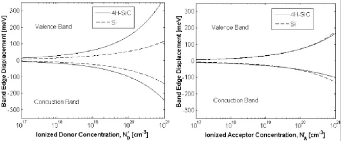
At the present, the fabrication of SiC devices with the given performances is not completely obvious. This fact is due to the lack of knowledge still existing in parameters related to SiO2/4H-SiC interfacial region and the sensitivity of some physical parameters
to temperature changes. Therefore, a set of investigative tools, designed especially for SiC devices, cannot be regarded as secondary objective. Following this need, in our research activity firstly predictive, numerical and analytical models, including temperature dependence, are used. This models able to explain the carrier transport in diffused regions and turns also useful for better understanding the influence of physical parameters, which depend in a significant way from the processed material, on device performances. These models are then assumed as objective functions in MOGA to determine the optimized physical and geometrical device parameters for a specific application. The models include also the device characterization at high temperatures to analyze the influence of thermal issues on the overall behavior up to temperature of 250°C. Secondly, with the aim to properly account for a realistic device, a combined model of both defect energy levels inside the 4H-SiC bandgap (deep and tail centers) and oxide-fixed traps has been incorporated in a more general, self-consistent model, allowing the analysis of the device behavior under the temperature and carrier-trapping effects.
Finally, with the imposition of right physical models, it is possible to use the versatility of the 2D Silvaco tool for extending the analysis and obtaining a physical insight on the
forward current regime (i.e. blocking voltage, threshold voltage, channel mobility, drain current, and on-state resistance).
dispositifs de puissance, l'analyse des MOSFETs à base de 4H-SiC est le sujet principal de ce document de doctorat. La thèse concerne en particulier la recherche utilisant des modèles numériques et analytiques, pour reproduire avec précision le comportement du MOSFET de puissance.
À l’heure actuelle, la fabrication de dispositifs en SiC avec les performances données n’est pas tout à fait évidente en raison du manque de connaissances concernant les effets des paramètres physiques et géométriques sur les performances du dispositif, en particulier de ceux liés à la région interfaciale SiO2 / 4H-SiC et la sensibilité de certains paramètres physiques aux changements de température. Par conséquent, un ensemble de simulateur conçus spécialement pour l’investigation des dispositifs SiC, ne peut être considéré comme un objectif secondaire. Pour répondre à ce besoin, notre activité de recherche utilise d’abord des modèles prédictifs, numériques et analytiques, y compris la dépendance à la température. Ces modèles capables d'expliquer le transport des porteurs s'avèrent également utiles pour mieux comprendre l'influence des paramètres physiques, qui dépendent de manière significative du matériau traité, sur les performances du dispositif. Ces modèles sont ensuite supposés être des fonctions objectives dans MOGA pour déterminer les paramètres optimisés des dispositifs physiques et géométriques pour une application spécifique. Les modèles incluent également la caractérisation du composant à haute température pour analyser l'influence des problèmes thermiques sur le comportement global jusqu'à une température de 250 ° C. En outre, dans le but de rendre compte correctement d'un dispositif réaliste, un modèle combiné des niveaux d'énergie des défauts à l'intérieur de la bande interdite 4H-SiC (centres profonds et de la queue) et des pièges fixés à l'oxyde a
Enfin, avec l’imposition de modèles physiques appropriés, il est possible d’utiliser la polyvalence de l’outil 2D Silvaco pour étendre l’analyse et obtenir un aperçu physique de l’effet de la concentration non uniforme de la région p-base et des propriétés de matériaux à K élevé pour déterminer le facteur de mérite fondamental du MOSFET 4H-SiC, (c'est-à-dire tension de blocage, tension de seuil, mobilité de canal, courant de drain et résistance à l'état passant).
ب فاشكتسا صئاصخلا ةيئابرهكلا ةزيمملا ل ديبرك نوكيليسلا ( SiC ) لمعتسملا رصانع ةعانص يف ةعاطتسلاا ، ربتعي ليلحت ةيبطقلا يداحلاا ةعاطتسلاا لحقم 4H-SiC MOSFETs وه عوضوملا يسيئرلا ةحورطلأ هاروتكدلا . ىلع هجو ،صوصخلا قلعتت ةحورطلأا ب يجهنملا ثحبلا مادختساب جذامنلا ةيددعلا ةيليلحتلاو ليلحتل كولس ةعاطتسلاا لحقم ةقدب . ايلاح ، عينصت ةعاطتسلاا لحاقم نوكيليسلا ديبراك مادختساب ءادأب زيمم سيل اًحضاو اًمامت ببسب صقن لوح تامولعملا ريثأت صئاصخلا ةيداملا ةيسدنهلاو ىلع ءادأ ه ، ةصاخو كلت ةقلعتملا ةقطنملاب لا ةينيب SiO2 / 4H-SiC و ةيساسح ضعب صئاصخلا تاريغتل ةجرد ةرارحلا . كلذل لا نكمي رابتعا قيقحتلا يف ةعاطتسلاا لحقم ىلع تاريثاتلا هذه اًفده اًيوناث . ىلارظنلاب هذه ةجاحلا ، يف انطاشن يثحبلا متي ًلاوأ مادختسا جذامن ةيؤبنت ةيددعو ةيليلحت ، امب يف كلذ دامتعلاا ىلع ريثات ةجرد ةرارحلا . هذه جذامنلا ةرداق ىلع حرش ةيلمع لا لقن لوحتتو اًضيأ ىلإ مهف لضفأ ريثأتل صئاصخلا ةيداملا ىلع ءادأ لحقملا . مث متي ضارتفا هذه جذامنلا فئاظوك ةيعوضوم يف نيسحتلا ةبراقم MOGA ديدحتل صئاصخ لحقملا يداملا ة يسدنهلاو ة ىلثملا قيبطتل نيعم . لمشت جذامنلا اًضيأ ةاكاحم لحقملل يف تاجرد ةرارح ةيلاع ليلحتل ريثأت تلاكشملا ةيرارحلا ىلع كولسلا يلكلا ىتح ةجرد ةرارح 252 ةجرد ةيوئم . ًايناث ، فدهب ليلحت لحقم يعقاو لكشب حيحص ، مت جمد جذومن دحوم تايوتسمل ةقاطلا ةبيعملا ( زكارم قمعلا ليذلاو ) خاخفلاو ةتباثلا ديسكلأاب يف جذومن ماع رثكأ اًقاستا اًيتاذ ، امم حمسي ليلحتب كولس زاهجلا تحت ريثأت ةجرد ةرارحلا . ا ًريخأ ، عم ضرف جذامنلا ةحيحصلا ، مت للاغتسا ددعت تامادختسا 2D Silvaco عيسوتل ليلحتلا لوصحلاو ىلع ةيؤر ةيدام لوح ريثأت زيكرت ةباشلاا ريغ مظتنملا ة يف لا ةدعاق p صئاصخو داوملا ةيلاع ةيذافنلا K يف ديدحت ايازم لحقملا ( ىلع ليبس لاثملا ، رايهنلاا رتوت ، ةبتعلا رتوت ، لا كرح ي ة يف ةانقلا ةمواقملاو .)
Contents
Acknowledgments ... I Abstract ... III Contents ... VIII General Introduction ... 1 Thesis outline ... 1 References ... 3Chapter I: State of the Art of Power MOSFET Devices I.1. Introduction ... 4
I.2. Power MOS component structures and operating principle ... 5
I.2.1. Power MOS devices ... 6
I.2.2 Integrated devices ... 9
I.3. Static and dynamic characteristics of power VDMOS transistor... 12
I.3.1. Breakdown voltage... 13
I.3.2. On state resistance ... 20
I.3.3. Silicon limit of vertical DMOS transistors... 24
I.3.4. Silicon limit in DMOS transistors ... 25
I.4. Wide band gap semiconductor materials for power electronics ... 26
I.4.1. Introduction ... 26
I.4.2. Compromise "specific On resistance / breakdown voltage" ... 28
I.4.3. SiC MOSFETs ... 29
I.5. Conclusion ... 36
References... 37
Chapter II: Modeling of the Electrical Behavior of 4H-SiC MOSFET II.1. Introduction ... 41
II.2. 4H-SiC MOSFET structure ... 41
II.3. Physical models ... 42
II.3.1. Transport properties ... 42
II.3.3. The apparent bandgap narrowing ... 48
II.3.4. 4H-SiC/SiO2 interface... 50
II.4. 4H-SiC MOSFET figure of merits ... 52
II.4.1. Breakdown voltage... 52
II.4.2. On-state resistance ... 53
II.4.3. Threshold voltage and drain current ... 54
II.5. Conclusion ... 55
References... 55
Chapter III: Physical and Geometrical parameters effect III.1. Introduction ... 60
III.2. Simulation analysis... 61
III.2.1. Analysis of temperature effect ... 62
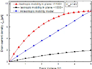
III.2.2. Isotropic and anisotropic mobilities study ... 64
III.2.3. Physical and geometrical parameters effect ... 65
III.3. MOGA-based optimization approach ... 69
III.3.1. 4H-SiC DMOSFET optimized design ... 71
III.4. Conclusion ... 75
References... 76
Chapter IV: Temperature and SiO2/4H-SiC interface trap effects on the electrical characteristics IV.1. Introduction ... 80
IV.2. MOSFET structure ... 81
IV.3. Characteristics in absence of trap effects... 82
IV.4. Analysis of trap effects at the SiO2/4H-SiC interface ... 85
IV.4.1. Tail traps ... 85
IV.4.2. Deep level traps ... 88
IV.4.3. Oxide-fixed traps ... 90
IV.5. Conclusion ... 93
References... 93
Chapter V: Effect of Nonuniform doped P base region and High-k Dielectrics V.1. Introduction ... 98
V.3. Results and discussion ... 99
V.3.1. Test of simulations setup ... 102
V.3.2. Impact of a non-uniform p-base doping concentration ... 103
V.3.3. High k/4H-SiC MOSFET analysis ... 107
V.3.4. Oxide/4H-SiC interfacial traps Effect ... 112
V.3.5. Temperature effect ... 115
V.3.6. Effect of fixed charge and thickness in HfO2 ... 118
V.3.7. Trap distribution model at HfO2/4H-SiC interface ... 120
V.3. Conclusion ... 123
References... 123
General Conclusion ... 129
During the last decade, use of 4H silicon carbide (4H-SiC)-based metal–oxide– semiconductor field-effect transistors (MOSFETs) for high-power, high temperature, and switching applications has been widely proposed.[1–5] Thanks to its outstanding physical and electronic properties (i.e., mechanical strength, thermal conductivity, and critical electric field) [6,7] silicon carbide has been recognized world wide as a promising material to improve device performance in terms of ON-state resistance, breakdown voltage, and switching capabilities. In particular, SiC MOSFETs are widely used as power devices in on board DC–DC converters for use in specific modules; For example, in Ref. [8], a boost based converter was proposed, describing the design of a zero-voltage zero-current switch (ZVZCS) suitable for high duty cycle and wide load currents; in Ref. [9], dual-SiC MOSFET modules were designed for use in the electric traction context; in Ref. [10], a dual active bridge (DAB) converter was implemented using 10-kV SiC MOSFETs; in Ref. [11] a high-frequency, 1-kW, 800 V output voltage boost DC–DC converter was developed. To meet the specific constraints related to modern power electronics, the design of 4H-SiC MOSFETs requires deployment of intensive modeling effort based in turn on numerical, analytical, and empirical calculations, carefully taking into account the different geometrical and physical parameters that affect device performance.[12–15].
Thesis outline
The aim of the work is to investigate, by means of a careful numerical simulation study, the electrical characteristics of a 4H-SiC MOSFET designed for low voltage ratings (150 V) over a wide range of temperatures. Without loss of generality with respect to different designs dimensioned for higher blocking voltages, explicit interface trap effects
temperature and neglecting defect and trap effects were presented in [16, 17] in order to emphasize, as stated previously, the use of fast and rugged 100-V-class switches. The obtained results clarify the role of the interface traps in reducing the carrier mobility in the channel region.
In the first chapter, we will present the state of the art of power MOS transistors with both vertical and lateral structures. The theoretical limit, called the "limit of silicon", the calculated specific on state resistance as a function of the breakdown voltage will be given in each case.
The second chapter describes the fundamental physical models taken into account during the simulations of the investigated 4H-SiC MOSFET and their reference parameters.
The third chapter will be devoted to the investigation of an optimized design of a 4H-SiC dual implanted MOSFET (DMOSFET) well suited for a specific application by means of a multiobjective genetic algorithm (MOGA). In more detail, starting from combined analytical and numerical analysis of the device current–voltage (ID–VDS) characteristic, both analytical and numerical models are used as objective functions in MOGA to determine fundamental design parameters that minimize the ON-state resistance of a device dimensioned for a blocking voltage (BVDS) in the range from 150 V to 800 V. The fourth chapter will be devoted to the investigation, by means of a careful numerical simulation study, the electrical characteristics of a 4H-SiC MOSFET designed for low voltage ratings ( BVDS = 150 V) over a wide range of temperatures. Without loss of generality with respect to different designs dimensioned for higher blocking voltages,
In chapter 5, after a short overview on the High-K material physics, a comparative evaluation of the gate deielectrics effect on the 4H-SiC MOSFET performances is carried out. This study is focused on the impact of thickness and fixed charge density. For this purpose, 2-D numerical simulations using a commercial two- dimensional (2D) technology computer-aided design (TCAD) physical simulator that provides the solution of Poisson’s equation and carrier continuity equations is performed.
We will conclude this manuscript by presenting some perspectives concerning the electrical modeling study of the 4H-SiC power MOSFET (Super Junction, Trench MOSFET,..).
[2] S. Mori, M. Aketa, T. Sakaguchi, Y. Nanen, H. Asahara, T. Nakamura, and T. Kimoto, IEEE Trans. Electron Devices 64, 4167 (2017).
[3] D. Bharti and A. Islam, IEEE Trans. Electron Devices 65, 615 (2018).
[4] K. Han, B.J. Baliga, and W. Sung, IEEE Electron Device Lett. 38, 1437 (2017).
[5] Y. Mikamura, K. Hiratsuka, T. Tsuno, H. Michikoshi, S. Tanaka, T. Masuda, K. Wada, T. Horii, J. Genba, T. Hiyoshi, and T. Sekiguchi, IEEE Trans. Electron Devices 62, 382 (2015).
[6] B.J. Baliga, Silicon Carbide Power Devices (Singapore: World Scientific, 2005). [7] B.J. Baliga, Fundamentals of Power Semiconductor Devices (New York: Springer,
2008).
[8] B.H. Choi, S.W. Lee, V.X. Thai, and C.T. Rim, IEEE Trans. Power Electron. 29, 5181 (2014).
[9] J. Fabre, P. Ladoux, and M. Piton, IEEE Trans. Power Electron. 30, 4079 (2015). [10] A.K. Tripathi, K. Mainali, S. Madhusoodhanan, A. Kadavelugu, K. Vechalapu, D.C.
Patel, S. Hazra, S. Bhattacharya, and K. Hatua, IEEE Trans. Power Electron. 32, 4231 (2017).
[11] X. Zhong, X. Wu, W. Zhou, and K. Sheng, IEEE Trans. Power Electron. 29, 5091 (2014).
[12] C.C. Hung, Y.S. Chen, C.T. Yen, C.Y. Lee, L.S. Lee, and M.J. Tsai, Mater. Sci. Forum 740, 711 (2013).
[13] A. Saha and J.A. Cooper, IEEE Trans. Electron Devices 54, 2786 (2007).
[14] G.D. Licciardo, S. Bellone, and L. Di Benedetto, IEEE Trans. Power Electron. 30, 5800 (2014).
[15] A. Merkert, T. Krone, and A. Mertens, IEEE Trans. Power Electron. 29, 2238 (2014).
[16] F. G. Della Corte, G. De Martino, F.Pezzimenti, G. Adinolfi, G. Graditi, IEEE Trans. Electron Dev. 65, 3352-3360 (2018).
[17] G. De Martino, F. Pezzimenti, F. G. Della Corte, G. Adinolfi, and G. Graditi, In Proc. IEEE Int. Conf. Ph. D. Research in Microelectronics and Electronics - PRIME, 221-224 (2017).
CHAPTER 1:
State of the Art of Power MOSFET Devices
Chapter1
State of the Art of Power MOSFET Devices
I.1. Introduction
In power electronics, bipolar transistors and thyristors were the first controllable power devices used in several power applications. However, these bipolar devices are not suitable for switching applications high frequency and require a complex control circuit providing non-energy negligible. The evolution of technologies in the field of MOS integrated circuits has allowed the development of families of power MOS transistors able to operate in high Frequency with simplified control through a grid insulated by a thin oxide. The conventional structure silicon power MOS transistor is a unipolar device which is widely used in high frequency switching power applications for breakdown voltages not exceeding 250 volts. The current in the power MOS transistor is a conduction current of a single type of carriers (the majority), there is therefore no evacuation delay due to the stored charge or to the recombination of the minority carriers as in the case of bipolar devices. Consequently, the switching speed of the power MOS transistors is much greater than that of the bipolar transistors. this property that makes the power MOS transistor the preferred device for high frequency switching applications.
The power MOS transistor consists of a multitude of elementary cells in parallel to allow the device to switch very large currents. Unlike bipolar transistors, paralleling MOS cells. Elementary is possible thanks to the coefficient of positive thermal drift of the on-state resistance of these cells. Therefore, the direct current distribution remains homogeneous between the constituent cells of the power MOS transistor. With respect to the power MOS technology, the power MOS transistor is fabricated using the P and N+
type planar dual diffusion process to realize the channel base P and N+ source areas.
Moreover, the name of these DMOS transistors is drawn directly from this double diffusion process, that is to say carrying out a P and N+ double diffusion through the
self-alignment of these diffusions makes it possible to adjust and control the length of the channel of the DMOS transistor to submicron dimensions.
For the first commercially available MOS power transistors, the power semiconductor manufacturers proposed several geometrical configurations of the source P cells of the transistor. The aim was to find the geometric shape of the source P scatter that allowed for the highest density of integration - the Z / S ratio of the perimeter to the surface of the chip - and hence the largest current per unit surface [1], [2]. For the same widths and depths of the source P diffusions, Hu [1] has demonstrated that the optimum resistances, representing the different zones of the passage of the current in the on state in the VDMOS structure, obtained by these different geometrical shapes are approximately the same if the ratios between the surface of the diffusion P and the surface of the cell are identical. On the other hand, technological progress has been made enabling the integration density to be increased by reducing the size of the constituent elementary cells of the power MOS transistor. There may be mentioned for example: the trench MOS transistor, also called UMOS [3] and the Motorola High Speed TMOS (HDTMOS) transistor [4].
In this chapter, we will discuss the main features of different power DMOS structures in the case of integrated and discrete devices. Specifically, we will give the so-called silicon limit that connects the breakdown voltage to the specific pass resistance, which is the product of the resistance in the on state by the active surface of the component, power DMOS transistors. Finally, given the technological progress made in the process of obtaining substrates made of wide-band gap semiconductor materials with better performances at very high temperatures, it seemed useful to recall here the impact of the use of these new materials on the compromise "specific pass resistance / breakdown voltage" of vertical power MOS transistors.
I.2. Power MOS device structures and operating principle
There are two types of power DMOS transistors: discrete transistors (vertical structures) and integrated transistors (lateral structures in general). LDMOS lateral structures (lateral DMOS) are used for low power radio frequency voltages applications [5].
I.2.1. Power MOS devices I.2.1.1. VDMOS transistor
Figure I.1 shows an elementary cell of the VDMOS transistor. This transistor is manufactured using the MOS dual diffusion process. The source and the gate are located on the surface of the chip while the drain is at the back of the chip. In the on state, the gate-source voltage Vgs is greater than the threshold voltage VT and an N-type inversion
channel is thus formed on the surface of the zone of the channel allowing the flow of current between the drain and the source. This current passes, in large part, in the volume of the structure through the N- drift zone. Part of this current goes to the surface in the channel and depends on the mobility of the electrons in the inverted layer. The inversion channel resistance is an additional limitation in the case of low voltage VDMOS transistors and is also important in the case of new power MOS made from silicon carbide because of the low mobility in the inverted layer. [6].
The N-drift zone assures the VDMOS transistor the ability to block the voltage in the off state. For a well optimized VDMOS structure [7, 8], the breakdown voltage depends on the doping and the thickness of the drift zone. In fact, to block very high voltages, the drift zone must be weakly doped and sufficiently wide to allow the space charge zone to expand. As a result, this wide and weakly doped zone becomes, in the on state, a very great resistance which can only be reduced by increasing the active surface of the device or by using new concepts such as the concept of superjunction by example. The use of high energy ionization materials can also to be a very good solution to this problem. There is therefore a compromise between the on-state resistance and the breakdown voltage of the VDMOS power transistors.
It may also be noted that the gate electrode here acts as a field plate and reduces the electric field at the surface of the "P-body / N-drift" junction. This is not without consequence because this gate electrode spread over the entire intercellular surface between the P source diffusions introducing a parasitic MOS capacitance between the gate and the drain. This capacitance, known as the Miller capacitance, causes a feedback between the output and input of the device and significantly reduces the transistor's transition frequency. To remedy this problem, it is possible for example to remove a portion of the grid [8, 9] above the epitaxial layer N-. In this case, a significant increase in the transition frequency of the transistor can be obtained. However, this elimination of a part of the gate causes a reduction in the breakdown voltage of the device, because of the strong electric field at the end of the gate metallization, and an increase in on state resistance because the length of the accumulated area is reduced. On the other hand, the equivalent resistance of the VDMOS transistor is composed of several resistors in series: channel resistance, accumulated resistance at the surface of the drift zone between the adjacent source P diffusions, JFET resistance of the region between the adjacent source P diffusions, resistance of the N-drift volume region, substrate resistance and contact resistances. The resistive effect of the JFET zone between the source P diffusions is all the greater as the doping of the epitaxial zone is weak, in the case of transistors intended to operate at high voltages, or if the distance between the source diffusions P is very weak. It is this last phenomenon, increasing the JFET resistance by decreasing the intercellular distance, which limits the integration density of power MOS devices
I.2.1.2. The trench MOS transistor
One solution to the problem of increasing the JFET resistance, limiting the integration density of the VDMOS structure, is the innovative structure, called the trench MOS structure, proposed by Ueda et al [10].to eliminate the JFET area and increase the integration density of the MOS elementary cells. This structure is widely used in the case of MOS low-voltage power transistors to reduce the on-resistance of the device and, therefore, increase the autonomy of nomadic systems of low power.
Figure I.2 shows a schematic section of the trench power MOS transistor. This structure is also called UMOS because of the U-shape of the buried grid under the source metallization. This structure makes it possible to increase the perimeter of the channel and to reduce the part of the N-drift zone under the source P diffusion which does not contribute to the passage of the current to the on state (problem of defocusing of the current lines, Figure I.1). Thus, the resistance of low voltage trench MOS transistors is very small, compared with VDMOS transistors of conventional structure with the same breakdown voltage.
The manufacturing technology of this type of transistor comes directly from the technology R.I.E (Reactive Ion Etching) [11] used in the manufacturing process of the memories DRAM.
Figure I.2: Schematic section of a cell of the trench MOS transistor [10].
The trench MOS transistor has a vertical configuration and current flows through the volume along the inverting channel which is now vertical. As in the case of the VDMOS transistor, the trench MOS transistor has a N-lightly doped zone to support the off-state voltage and is constituted by the paralleling of several MOS cells ensuring the passage of a strong current. in the passing state. At the level of the dynamic performances, one can notice that there is no improvement at the level of the Miller grid-drain capacity because of the part of grid, above the drain, buried under the diffusion P source. For the two types of vertical transistors mentioned here, there is no current limitation and it is possible, a priori, to set up as many elementary MOS cells in parallel to ensure the passage of the desired current in the on state. With regard to the breakdown voltage, there is no fundamental limitation, but the resistive effect of the drift zone, broad and
weakly doped in the case of high voltage MOS, can cause conductive losses which can cause the destruction of the power transistor.
I.2.2. Integrated devices
The advantage of these coplanar structures is that they can be integrated with the processing part of the analog or digital signal for the development of the system on a chip (System-on-Chip: SoC). The advantage of this integration lies in the elimination of parasitic elements due to the connecting wires in the discrete circuits, suppression of interface circuits between the power and the control and the reduction of the weight and the cost of the power electronic function performed on a chip. The most known technologies are: '' SmartMOS '' used by Freescale and ST Microelectronics. The most used integrated device is LDMOS because it is able to operate at very high frequencies [5] and because its three electrodes are at the surface, which facilitates its integration.
I.2.2.1. LDMOS transistor
Figure I.3 shows a schematic section of the conventional LDMOS transistor. The breakdown voltage is limited in this structure at voltages of the order of 250 volts. Indeed, the breakdown in this structure usually occurs at the end of the gate metallization (because of the small thickness of the gate oxide) or at the PN-cylindrical junction. It depends mainly on the doping of the drift zone and the distance Ld between the end of the gate metallization and the beginning of the opening of the drain diffusion [12, 13].
In addition, the presence of the three electrodes on the upper face of the chip does not facilitate the densification of the cells in parallel to form the power LDMOS transistor. The source and the drain are most often in the form of interdigitated parallel bands. The buried layer N + makes it possible to limit the extension of the space charge area in the region N- and to avoid the piercing of the substrate P. It can also make it possible to cancel the gain of the parasitic transistor PNP between the substrate and the source P diffusion of the power MOS transistor. The electric current passes on the surface of the structure and depends on the distance Ld; this distance is also called the length of the drift zone. The lower the distance, the weaker the resistance of the component. Unfortunately, the breakdown voltage decreases as Ld decreases and it has been demonstrated by two-dimensional numerical simulations [13] that there is an optimum drift distance providing a maximum breakdown voltage for a given drift doping. This therefore limits the integration density because the choice of the drift distance, which is on the surface of the structure, will be imposed by the compromise between the breakdown voltage and the specific passing resistance. Thanks to a very low Miller capacity compared to the vertical structure, the LDMOS is the device of choice for radio frequency applications [14].Many variants of the structure of the LDMOS transistor have been proposed to improve its breakdown voltage; we can cite for example:
a) LOCOS LDMOS transistor (LOCal Oxidation in Silicon): in this structure, the electric field at the end of the gate metallization is greatly reduced by local oxidation of the silicon. The major problem of this structure is the degradation of the current passing surface in the on state and, therefore, a significant increase in specific pass resistance compared to that of conventional LDMOS structures.
b) The LDMOS Resurf (Reduced Surface Field) (Figure I.4): this structure is obtained by replacing N-epitaxy on substrate N + by an N- epitaxial layer on a P- substrate.
The substrate P- must be connected to the source, through the source P diffusion, so
that the plane diode thus formed is polarized in reverse and supports, under certain conditions, the drain source voltage. If the Resurf structure is well designed, the N- zone must be completely depleted before the surface area has a point where the field reaches the critical breakdown field. If, in addition, the distance between the source and the N +
drain diffusion is such that the drilling of the N + drain zone is effective, the breakdown can take place at the plane junction NP - thus making it possible to significantly improve the voltage of breakdown compared to the classic LDMOS structure. Another advantage of this structure is that the resistance in the on state remains identical to that of the conventional LDMOS structure while the breakdown voltage is significantly improved. This technique has allowed monolithic power ICs to exceed 250 Volts breakdown voltages.
I.2.2.2. The VDMOS transistor up-drain
The structure of the VDMOS up-drain transistor (Figure I.5) resembles the structure of the vertical NPN bipolar transistor with the drain acting as the collector. This solution has been proposed to solve the problems of insulation appearing between two VDMOS manufactured on the same plate. In this structure, the current passes, in large part, between the drain and the source vertically. The buried layer N + serves to collect the electrons and drain them to the drain on the surface of the chip through the well N + of the drain. Unfortunately, this too long electron path increases the on-state resistance of this type of power MOS transistor and, therefore, the conduction losses of the component.
I.2.2.3. LUDMOS transistor
In order to improve the breakdown voltage of lateral MOS structures, M. Zitouni [13] proposed an LDMOS structure integrating an oxide trench in the drift zone at the end of gate metallization. This structure (figure I.6), called LUDMOS, makes it possible to reduce the electric field on the surface. Zitouni then proposed, trying to reduce the specific pass resistance, several variants [13] of this structure by eliminating the distance between the trench and the drain (structure 2), then filling the trench with the gate polysilicon (structure 3). ) and, finally, by overdoping the surface of the drift zone (structure 4).
Despite the path length of the current flow, this structure makes it possible to obtain a better compromise between the specific on resistance and the breakdown voltage compared to a conventional DMOS structure with the same breakdown voltage. Using two-dimensional simulations, it has been shown [13] that for a breakdown voltage of 60 volts, the specific pass resistance is only 0.6 mΩ.cm 2 against 1.57 mΩ.cm 2 for a conventional 60 V LDMOS structure, a reduction of more than 60%.
Figure I.6: Schematic section of a LUDMOS transistor [13].
I.3. Static and dynamic characteristics of power VDMOS transistor
As in the case of the other silicon power structures, the power MOS transistor must integrate in its structure a weakly doped zone, N- in the case of the N-channel VDMOS transistor, to support the voltage in the off state. The breakdown voltage depends on the thickness and doping level of this N-drift zone.
In this paragraph, we will focus on the study of the breakdown voltage, called the first breakdown voltage, equivalent to the maximum drain-source voltage Vds for a
gate-source voltage Vgs zero. The transistor is in the off state and no current flows between the drain and the source. Because doping of the source P diffusion is greater than doping of the N-drift zone, the depletion zone extends mainly in the weakly doped N - drift zone. If the structure is well designed [7, 8], we can consider that the breakdown takes place at the plane junction "P-body / N- drift '. In this case, we can assimilate the structure of the transistor VDMOS with a reverse biased PN-N+ diode.
I.3.1. Breakdown voltage
In the off state and for a zero Vgs voltage, the drain voltage cannot evolve beyond a
maximum voltage known as the first breakdown voltage. At the approach of this limit, the breakdown occurs by avalanche and the drain current increases inconsiderately.
The breakdown of the VDMOS structure has multiple origins -figure I.7-: 1) lateral zones where the effects of curvatures of the junctions are predominant, 2) frontal zones where the extension of the space charge can be or not be limited, 3) surface areas of the lightly doped region covered with gate oxide and 4) the oxide itself. These problems have been largely addressed by [7]. Several junction guarding techniques are used to avoid premature breakdown of the structure by attempting to minimize the surface effects and to lengthen the radius of curvature of the junctions, inevitable in the case of diffusions, to try to reach the theoretical breakdown. of the planar junction [7, 15, 16].It should be noted that the gate electrode spread over the entire intercellular surface also reduces the field to the surface of the structure. In addition, by a judicious choice of the intercellular distance, self-shielding can be obtained to protect the gate oxide [7, 8].In practice, junction guarding techniques are used to allow the structure to hold up to 90% of the breakdown voltage of the plane junction [7].
For a well-designed VDMOS structure, it can therefore be considered that the breakdown takes place in the volume of the structure at the plane junction "P-body / N-drift". This breakdown voltage depends on the thickness and the doping of the drift zone. For an inverse polarized one-dimensional PN diode, the breakdown conditions are governed by the avalanche multiplication mechanism. It is considered that these conditions are satisfied when the ionization integral (In or Ip) is equal to unity, ie:
dx dx I X W p n W n n
exp
0 (I.1)
dx dx I X p n W p p
0 0 exp
(I.2)where αn and αp are respectively the ionization coefficients of electrons and holes.
These coefficients αn and αp represent the probable number of ionizing collisions
experienced by an incident carrier, hole or electron, per unit of path length. According to Sze [17], these two equations are strictly equivalent as regards the determination of breakdown voltages; one or the other of them can be used indifferently because they reach unity for the same tension. For the VDMOS transistor that interests us, and using a two-dimensional simulation software such as ATLAS (SILVACO tool), the breakdown voltage is determined by calculating the ionization integral from the αn coefficients. and
αp whose values are different, depending on the model chosen.
For the analytical calculation, one of the major problems is that of the formulation of the ionization coefficients. Indeed, these coefficients are expressed as a function of the electric field in the following form:
(I.3) To facilitate this task, Mac Kay [18] has shown that the ionization coefficients can be approximated by simpler functions which are polynomial expressions of the type:
1 7 .E A cm n
(I.4)
1 7 .E A cm p
(I.5)where A' and A" are two constants whose values have been proposed respectively by: 35 10 . 8 , 1 A A A (I.6) 35 10 . 6 , 3 A (I.7) 35 10 . 3 , 0 A (I.8)
Note that the proposed values for A' and A'' by Fulop are identical. On the other hand, Gharbi proposes two different values for A' and A'' Other authors have proposed different values but we will retain the values proposed by Gharbi because they represent an average for these proposed values.
There are two cases before the breakdown of the PN-N+ diode :
1) case of the infinite junction in non-limiting or non-piercing (NPT): in this case, the space charge area is less than the thickness of the N- zone and the shape of the electric field is triangular -figure I.8-:
2) Punch-through case (PT): The space charge area is greater than the thickness of the N- zone and the shape of the electric field can be considered as' 'trapezoidal' -Figure I.9-.
Figure I.9: Case of limit junction or "Punch Through" (PT) drilling [8].
I.3.1.1. Case of an infinite plane junction in non-limitation '' No Punch Through ''
In the hypothesis of an abrupt flat P+ N dissymmetrical junction, the integration of the
Poisson equation makes it possible to determine the expression of the electric field:
2
. . h H x N q x E si n d (I.9)(H-h2) is, in this case, considered to be the maximum extension of the space charge area
(SCA) of an infinite plane junction -figure I.8-
Based on equations (I.4), (I.5) and (I.9), the calculation of the ionization integral using equation (I.1) or (I. 2) makes it possible to express the breakdown condition of the PN junction as a function of the parameters of the structure:
2
7 0 . . . . 8 ln A A qN H h A A si d (I.10)On the other hand, the maximum extension (H-h2) of the space charge of the abrupt
plane NP junction, that is to say at the moment of breakdown, is given by [17]:
2 1 0 2 . . . . 2 DBR d si V N q h H (I.11)By combining the expressions (I.10) and (I.11), the extension of the maximum space charge (H-h2) is thus obtained as a function of the breakdown voltage VDBR:
6 7 6 1 2 . ln . 16 VDBR A A A A h H (I.12)Then the breakdown voltage VDBR as a function of the Nd doping:
4 3 4 1 3 0 . ln . . . . . 2 1 si d DBR N A A q A A V (I.13)Using the values of A 'and A' 'proposed by Gharbi, we can calculate the expressions of the breakdown voltage and the maximum extension of the space charge as a function of the doping for an infinite plane junction with no limitation of the space charge area:
4 3 13 . 10 . 72 , 5 d DBRVolts N V (I.14)
8 7 10 2 2,7.10 . H h Nd cm W (I.15)I.3.1.2. Case of a plane junction in '' Punch Through '' limitation
Given relations (I.4) and (I.5), the integral (I.2) can be written as:
W x p A E A A E dx dx I 0 0 7 7 . exp . . (I.16)W is the space charge extension, in this case it is equal to (H-h2), according to figure
I.9. The electric field E is obtained by the one-dimensional integration of the Poisson equation and is written in the form:
x qN
W x
E SI d 1 0 . . . (I.17)W1 is the maximum extension of the space charge defined in Figure I.9 in the case of a
Since the integral (I.16) is equal to unity, its resolution leads to the following breakdown criterion:
A A N q A A h H W W d si ln . . . . . 8 7 7 0 8 2 1 8 1 (I.18) For convenience of writing, we assume:
A A N q A A C et h H W d si ln . . . . 8 7 7 0 2 (I.19)Equation (I.18) can then be written as:
W W
C W8 1 8 1 (I.20)
The expression (I.20) does not admit a "direct" analytical solution. To solve it, we use the following iterative procedure:
At first order: for W1 = W' we get the solution:
8 1 1
1 C
W (I.21)
Second order: replace the first solution in equation (I.20), which gives:
8 1 8 8 1 2 1 C C W W (I.22)
In the third order, replace the second relation in equation (I.20). We obtain as follows: 8 1 8 8 1 8 8 1 3 1 C C C W W W (I.23)
Which gives order n the following solution:
8 1 8 1 1 1 C W W W n n (I.24)To study the influence of this method of resolution on the resistance in tension, we calculate the curves of the resistance in tension as a function of the doping and this for several values of the thickness of epitaxial. The one-dimensional resolution of the Poisson equation leads to the following expression:
1 2
2 0 . 2 . 2 . . . h H W h H N q V si d DBR (I.25)figure I.10 shows the characteristics of the breakdown voltage as a function of doping and epitaxial thickness (H-h2) in the case of the planar junction in limitation. The curves
plotted for n = 1 have maxima whose existence is related to the approximation made on the order of the solution. When the order n increases, the curves have a horizontal asymptote which is the limit solution (n -> ∞), which can also be calculated analytically by extending the term of the Nd doping towards zero:
7 6 7 1 . ln 1 H A A A A VDBR (I.26)
Figure I.10: Breakdown voltage of the PN-N + junction "Punch Through" limitation [8].
The thickness of the N-epitaxial zone in the case of the limiting structure (PT) will be smaller than that in the case of non-limitation (NPT). Therefore, the on-state resistance will be lower in the case of depletion region limitation than in the case of non-limitation. In the case of IGBTs, there are two PT and NPT structures on the market. PT IGBTs have reduced conduction losses while NPT structures are faster with low switching losses.
New IGBT structures have emerged in recent years to try to combine the advantages of both PT and NPT structures (LPT: Light PT for Mitsubishi and SPT: Soft PT for ABB for example).
I.3.2. On state resistance
The on-state resistance of the power MOS transistor is defined as the total resistance that occurs between the source and the drain as the transistor drives in a linear, low-drain-source voltage regime. Its value can be calculated by determining the ratio:
0 ds V ds ds on I V R (I.27)
In practice, its value is given for a grid voltage of 10 volts.
This resistance (figure I.1) is equivalent to the sum of several resistors in series: the resistance of the source N+ diffusion, the resistance of the channel, the accumulated
resistance in surface of the intercellular zone under the gate, the resistance JFET of the zone drifting between the adjacent source P diffusions, the drift resistance, the substrate resistance, the metallization resistors and the resistances of the electrical connection wires to the housing. For high-voltage VDMOS devices, the drift resistance represents more than 90% of the component's on-state resistance. On the other hand, in the case of low voltage VDMOS transistors, the substrate resistance is not negligible and the channel resistance and the access resistance (accumulated resistance + JFET resistance) become comparable to the drift resistance.
I.3.2.1. Channel Resistance
The resistance of the channel is calculated by determining the ratio:
0 ch V ds ch ch I V R (I.28)
where Vch is the voltage between the drain and the source at the terminals of the
inversion channel and Ids is the drain current [20].
In the hypothesis of uniform doping in the channel, the expression of the resistance of the channel can be given by:
T gs F gs ox ch V V V L Z C R . . . . 2. 1 0 (I.29)
where μ0 is the low electric field mobility, Cox is the oxide capacity, ψ is the transverse
reduction potential of the mobility, Vgs 'is the effective gate voltage (Vgs' = Vgs + Qss /
Cox-φms), VT is the threshold voltage of the transistor and ΦF is the Fermi potential. Z is
the perimeter of the channel and L is the length of the channel. According to this expression, we can see the advantage of increasing the perimeter of the channel in the case of MOS structures of low voltage where the resistance of the channel is not negligible.
I.3.2.2. Accumulation resistance
The access Ra of a power MOS transistor is the equivalent resistance of two resistors in series: the resistance of the layer accumulated at the surface in the intercellular zone (Racc) and the resistance JFET (RJFET) between the diffusions P source adjacent.
Several authors have proposed formulas for calculating this resistance [8, 21, 22]. The expression of the access resistance can be written as [8]:
0
2 0 . 2 . . 2 . . . . 2 Z L W h V V V A C L k R a D T gs F gs ox acc a a (I.30)where La is the length of the accumulated zone, h2 is the depth of the source P diffusion
and W0 is the extension of the space charge area in the N-drift JFET zone. μ0acc is the low
field mobility in the accumulated layer,
Λ is the mobility reduction potential in the accumulated layer [22] and ρD is the
resistivity of the N- drift zone. K is a corrective factor that takes into account the
two-dimensional nature of the passage of the channel current to the drift zone through the JFET pinch zone.
In the expression (I.30), the first term is equivalent to the resistance of the accumulated zone, while the second term corresponds to the resistance of the JFET region.
T.P. Pham [21] and J-L. Sanchez [22] proposed a calculation method based on a distributed diagram of the access zone in vertical and horizontal directions. In this case, the expression of the access resistance Ra can be given by:
. . . . . . 2 2 a d n a L Z N q h R (I.31)
μn is the mobility in the volume of the drift zone N- and λ 'is a parameter which depends
on the gate-source voltage Vgs, the doping of the drift zone N-, the depth of the source
diffusions P and the mobility.
I.3.2.3. Drift resistance
It is the resistance of the layer that supports the voltage in the off state. As a first approximation, it can be considered that the current passes uniformly in this zone and the drift resistance is equivalent to an ideal drift resistance which can be calculated according to the conventional relation of a semiconductor bar:
. . . . 2 S N q h H R d n d (I.32)
where S is the surface of the elementary cell
The two-dimensional nature of the defocusing phenomenon of the current lines in the volume of the material does not allow an analytical approach adapted to the study of all the cases of surface geometry and thickness of the epitaxial layer. Considering the defocusing of current lines under source P scattering at a 45 ° angle (Figure I.1), B. J. Baliga [8] proposed the following expression:
0 2 0 ln . . . . 1 W L h H W L Z N q R a a d n a (I.33)There are other analytic expressions for calculating this resistance according to several elementary cell geometries. In our case, we will use the formula (I.33) which gives a good approximation of the drift resistance of the FLIMOS transistor. The current in the drift zone passes largely in the region under the grid (figure I.1) thus creating an unused zone under the source P scattering [23]. Thanks to the technological progress of densification of the elementary cells of the MOS transistor, this unused area has been greatly reduced and, consequently, the specific pass resistance of the power MOS device has been improved [23]. More recently, innovative structures, based on the concept of super junction and the concept of floating islands, have allowed a significant improvement in drift resistance. The drift resistance depends mainly on the doping and
the thickness of the drift zone which fixes the breakdown voltage of the component. It is therefore also possible to reduce this resistance by introducing broad bandgap semiconductor materials with high ionization energy. The higher this energy, the lower the drift resistance. This is one of the reasons why new materials with high ionization energy are being studied to develop MOS transistors of low resistance power in the on state and which can operate in addition to high temperature through their wide bandgap.
I.3.2.4. Other resistances
The other resistors of the VDMOS structure are: N+ source scattering resistance,
substrate resistance and contact resistances. The resistance of the N+ source scattering
is negligible in the face of other resistances because of high N+ doping. On the other
hand, the resistance of the substrate is not negligible in the case of low voltage transistors because the substrate must be sufficiently thick to allow the robustness of the wafer during the manufacturing steps of the component. The resistance of the substrate can be calculated using the formula for calculating the resistance of a Nsub semiconductor doping bar and thickness Esub:
S N q E R sub nsub sub sub . . . (I.34)
In the case of small power MOS transistors intended for portable applications (breakdown voltage of the order of 30 volts), the connection resistances are no longer negligible in the face of the silicon resistors thanks to the new high power density MOS structures. integration such as trench MOS transistors for example. It is for this reason that several power device manufacturers have changed how to connect their chips, in the case of small power devices, in order to solve the various problems due to the standard housings used: connection resistance, parasitic inductance and thermal resistance.
I.3.3. Silicon limit of vertical DMOS transistors
In theory, it can be assumed that the on-state resistance of the power MOS transistor depends on the number of cells elementary elements in parallel constituting this component. This implies that by increasing the number of cells in parallel, the on-state
resistance of the power MOS transistor can be reduced. But this reduction will be accompanied by a chip surface too important. It is therefore the product (Ron.S) of the
resistance in the active state by the active surface, called specific resistance-resistance or "specific on-resistance", which is the parameter the most important for power MOS devices. Considering that the on-state resistance is equivalent to the ideal drift resistance, ie neglecting the other resistances, the ideal specific pass resistance can be given by: . . . . 2 d n on N q h H S R (I.3)5
The relation linking the mobility to the breakdown voltage can be given by [24]:
2 1 1
2 0,1 . 10 . 1 , 7 . . DBR n cm V S V (I.36)In the case of the limitation of the ECA, Gharbi [7] considered that the electrical breakdown field at the main junction remains equal to that of the non-limiting junction and expressed the "thickness-doping" torque of the drift zone according to the following relationships:
6 7 6 2 cm 1,87.10 .VDBR h H (I.37)
3 4 18 3 . 10 . 85 , 1 DBR d cm V N (I.38)We considered the case of the limitation which gives the smallest thickness of the epitaxial zone and thus the lowest resistance in the on state.
Using equations (I.35), (I.36), (I.37) and (I.38), we find:
2
9 2,4 . 10 . 9 , 8 . . DBR on S cm V R (I.39)This equation expresses for a vertical MOS component, or more generally for vertical unipolar power devices, the minimum resistance that cannot be exceeded for a given breakdown voltage.
B.J. Baliga gave [8] a formula different from equation (I.39), with a calculation based on non-uniform drift doping, in which the breakdown voltage is at power 2.5:
2
9 2,5 . 10 . 3 , 8 . . DBR on S cm V R (I.40)However, the values of the specific pass resistance calculated by formulas (I.39) and (I.40) are very close. As a result, we will use equation (I.39).
By protecting the main junction of the vertical DMOS structure, new structures have significantly reduced the drift resistance and, consequently, the specific pass resistance of the unipolar power devices. However, equation (I.39) is a very difficult limit to overcome or "break" in the case of VDMOS transistors of low voltage power because the drift resistance represents, in this case, only 30 to 40% of the total resistance of these conventional structures. On the other hand, this limit can be exceeded by new structures in the case of high voltage MOS devices because the drift resistance represents, in this case, more than 90% of the total resistance in the on state. Several research projects, on new silicon structures or new silicon substitution materials, have been conducted in recent years to try to approach or "break" this so-called silicon limit. Thus, new power MOS structures have been introduced; for example, superjunction structures [25] and floating-island structures [26, 27, 28, 29].
I.3.4. Silicon limit in DMOS transistors
The conventional LDMOS structure is intrinsically limited to breakdown voltages not exceeding 250 volts. To exceed this limit, the LDMOS Resurf structure is used in general. We will therefore retain this last structure to define the so-called silicon limit in the case of lateral DMOS structures. Fujihira [25] proposed an estimation of the silicon relation for conventional Resurf structures:
12 2 5 6 2 . . 10 . 04 , 2 . . epi DBR on S cm W V R (I.41)Wepi is the thickness of the epitaxial zone (Figure I.4). This thickness depends on the
I.4. Wide band gap semiconductor materials for power electronics
I.4.1. IntroductionThe need for new applications of power electronics, for example in hybrid vehicles, requires reliable, fast electronics, low conduction and switching losses and can operate at very high temperatures. Silicon, currently the most used microelectronic material, can not meet these requirements because of these physical and thermal characteristics that limit its use in many power applications and in particular in automotive electronics. It is therefore to new semiconductor materials with a wide bandgap that research has focused in recent years to meet the requirements mentioned above. Indeed, several research projects are currently being conducted to promote broad bandgap semiconductor materials that can improve the static and dynamic performance of power devices. It is well known that, due to the thermal agitation in the crystal lattice of a semiconductor material, the height of the band gap decreases as the temperature increases and, therefore, this material can become conductive at high temperature. The choice of wide bandgap semiconductor materials is therefore the solution to have an electronics capable of continuing to operate at high temperature. In addition, the critical field of breakdown of the semiconductor material is related to the height of the forbidden band. The higher the height of the band gap, the greater the critical field of breakdown. Therefore, these large bandgap semiconductor materials will be very interesting for power electronics applications because to maintain high voltages in the off state, the operation of the drift zone will be greatly improved and the thickness of this zone will be very thin. In this case, the drift resistance will no longer be a handicap for high voltage (> 250 Volts) MOS devices in wide bandgap semiconductor materials. It can also be noted that the resistance of the connection wires and the resistance of the channel will no longer be negligible for breakdown voltages below 1 kV because of the sharp reduction in drift resistance.
Among the promising silicon substitution materials in high temperature power applications are silicon carbide (SiC), gallium nitride (GaN) and diamond. In the case of silicon carbide power MOS devices, for example [6], [30], the low mobility in the inversion layer remains one of the major problems to be solved for high voltage MOS
devices. It has been shown [30] that the channel resistance can represent 44% of the on-state resistance whereas the drift resistance only represents 17% of this resistance for a silicon carbide power MOS transistor 660 volts. This experiment shows the need for a new definition of the material limit in the case of unipolar devices made from wide bandgap semiconductors because the drift resistance no longer represents the important device up to the voltages of the order of 10 kV.
In practice, Schottky diodes made of silicon carbide are marketed for breakdown voltages exceeding 500 volts with a high current in the on state. For example, the company Infineon offers Schottky diodes 600 volts silicon carbide with a maximum current in the passing state of 100 amps (characteristics of this diode can be found on the website of the company: device under reference IDT02S60C).The electron saturation velocity of wide-bandgap semiconductor materials is much greater than that of silicon and, therefore, it is possible that the devices made from these materials are capable of operating at high frequencies. In addition, the stored load and the recovery time will be considerably reduced thanks to the small thickness of the drift zone.
A last important parameter for these silicon substitution materials is the thermal conductivity. The higher the thermal conductivity, the lower the thermal resistance and, therefore, the material can easily transmit heat to the outside. This allows a slow increase in temperature in the power device. Table I.1 gives the main physical characteristics of broad bandgap semiconductor materials. There are two types of silicon carbide substrates: 4HSiC and 6H-SiC. Prior to the introduction of 4H-SiC in 1994, the only available silicon carbide substrate was 6H-SiC. These two materials have similar properties except the mobility of electrons which is in the case of isotropic 4H-SiC and greater than the anisotropic mobility of electrons in the case of 6H-SiC.
According to Table I.1, diamond is the reference semiconductor material due to its high critical breakdown field, higher electron mobility than other materials and the highest thermal conductivity. Gallium Nitride has the lowest thermal conductivity, compared to other semiconductor materials, including silicon, but it can be very interesting for optoelectronic power applications thanks to its direct gap and its critical field of breakdown 6 times higher than critical field of silicon.
Table I.1: Key characteristics of SiC vs. other semiconductor materials [8].
Si GaAs 4H-SiC GaN Diamond
Eg@300K (ev) 1.1 1.4 3.2 3.4 5.45 EC (MV/cm) 0.3 0.4 2.2 2 10 Vsat (×107 cm/s) 1.0 2.0 2 2.5 2.7
µn@N=1016 cm-3
(cm2/VS) 1500 8500 720 1000 2200µp@N=1016 cm-3
(cm2/VS) 480 400 120 30 850 εr 11.9 13.1 9.7 8.9 5.5 λ (W/cm K) 1.5 0.5 5 1.3 22I.4.2. Compromise "specific On resistance / breakdown voltage"
For a PN-junction, the breakdown voltage depends on the critical field of breakdown of the semiconductor material used:
d c r DBR N q E Volts V . . 2 . . 2 0 (I.42)where ε0 (F/cm) and εr represent the permittivity of the vacuum and the semiconductor
material used respectively, q the elementary charge of the Coulomb electron, Nd the
doping of the N-zone in cm-3 and Ec the critical field of breakdown in V/cm.
The ideal specific passing resistance of drift in the on state can be given by the following relation [25]:
![FIGURE I.12 - Schematic sectional view of a vertical SiC MOSFET structure with a trench gate [3]](https://thumb-eu.123doks.com/thumbv2/123doknet/14896621.651867/43.892.292.653.468.735/figure-schematic-sectional-view-vertical-mosfet-structure-trench.webp)

![Figure III.2: Gate-source voltage versus the forward drain current for [300 K- 500 K]](https://thumb-eu.123doks.com/thumbv2/123doknet/14896621.651867/77.892.268.667.599.896/figure-gate-source-voltage-versus-forward-drain-current.webp)