The MIT Faculty has made this article openly available.
Please share
how this access benefits you. Your story matters.
Citation
Chakraborty, Chitraleema et al. “Advances in quantum light
emission from 2D materials.” Nanophotonics, 8, 11 (August 2019):
2017–2032 © 2019 The Author(s)
As Published
10.1515/NANOPH-2019-0140
Publisher
Walter de Gruyter GmbH
Version
Final published version
Citable link
https://hdl.handle.net/1721.1/129643
Terms of Use
Creative Commons Attribution 4.0 International license
Review
Chitraleema Chakraborty*, Nick Vamivakas and Dirk Englund
Advances in quantum light emission from 2D
materials
https://doi.org/10.1515/nanoph-2019-0140
Received May 10, 2019; revised June 26, 2019; accepted July 12, 2019
Abstract: Two-dimensional (2D) materials are being actively researched due to their exotic electronic and opti-cal properties, including a layer-dependent bandgap, a strong exciton binding energy, and a direct optical access to electron valley index in momentum space. Recently, it was discovered that 2D materials with bandgaps could host quantum emitters with exceptional brightness, spec-tral tunability, and, in some cases, also spin properties. This review considers the recent progress in the experi-mental and theoretical understanding of these localized defect-like emitters in a variety of 2D materials as well as the future advantages and challenges on the path toward practical applications.
Keywords: 2D materials; defects; single-photon emission; quantum-confined exciton; transition metal dichalcoge-nides; hexagonal boron nitride.
1 Introduction
Two-dimensional (2D) materials exhibit strong light-matter interaction, giving rise to their large exciton binding energy, linear and nonlinear optical properties, and spin-valley coupling [1]. They are a highly attractive plat-form for fundamental science as well as for applications. Further, the seamless integration of 2D materials with a wide variety of photonic platforms offers opportunities for engineering nanoscale light-matter interaction [2–4]. In
parallel, five independent teams of researchers had iden-tified isolated quantum emitters in a monolayer transition metal dichalcogenide (TMDC) at low temperatures [5–9]. Thereafter, room temperature single-photon emission was also discovered in hexagonal boron nitride (hBN), an insu-lating 2D material [10]. Solid-state quantum emitters are at the forefront of quantum computing and sensing, owing to their prospects of scalability, robustness, and ease of handling [11–13]. Graphene quantum dots (QDs) have also attracted interest in the scientific community due to their high transparency and large surface area. A number of remarkable applications in energy conversion, display, and biomedicine have been proposed [14]. In addition, semiconducting 2D materials offer an extra advantage such that confinement can be designed via an electro-static field [15] or strain field [16, 17] that would locally modify the bandgap. Furthermore, TMDCs have several isotopes with vanishing nuclear spin compared to III to V semiconductors [18, 19], thus lacking hyperfine interac-tions with the electronic spin. Owing to the stronger spin-valley coupling in monolayer TMDCs, spin-valley hybridization in TMDC quantum emitters should be quenched and the localized emitters can inherit the valley physics of the host 2D material [20]. Quantum emitters in 2D materials would provide a smaller footprint than most conventional solid-state quantum emitters, making them easier to inte-grate with existing photonic and optoelectronic structures with better light extraction and efficient modulation. This review discusses the recent advances made in the field of quantum optics of these localized emitters since their discovery.
2 Quantum light from 2D
semiconductors and insulators
Quantum light emission in 2D semiconductor platform was first demonstrated in monolayer tungsten
disele-nide (WSe2) by five independent research groups in 2015
[5–9]. Before that, valley excitons in 2D materials were studied for 5 years since the discovery of optically active
*Corresponding author: Chitraleema Chakraborty, Electrical
Engineering and Computer Science, Massachusetts Institute of Technology, Cambridge, MA 02139, USA; and John A. Paulson School of Engineering and Applied Sciences, Harvard University, Cambridge, MA 01238, USA, e-mail: [email protected]. https://orcid.org/0000-0003-2393-0481
Nick Vamivakas: The Institute of Optics, University of Rochester,
Rochester, NY 14627, USA
Dirk Englund: Electrical Engineering and Computer Science,
Massachusetts Institute of Technology, Cambridge, MA 02139, USA
Open Access. © 2019 Chitraleema Chakraborty et al., published by De Gruyter. This work is licensed under the Creative Commons Attribution 4.0 Public License.
atomically thin MoS2 [21]. However, when studied at low temperature (4 K) and very low laser excitation power (approximately nanowatts), spatially localized emis-sions (Figure 1A) exhibiting spectrally narrow lines of ~50 to 500 μeV (10 μeV with resonant excitation [22]) were observed in photoluminescence (PL) emission from certain locations of the flake near edges, wrinkle, or nano-bubbles in the monolayer [23]. Although the detailed microscopic origin of the quantum emission in 2D TMDCs is still not understood, highly localized strain gradients are often correlated with the physical origin of these emit-ters (see details in Section 3.1). One plausible explanation is that excitons can become trapped into such localized strain gradients created by these imperfections in the
flake. Crystallographic defects may also play a role in sin-gle-photon emission in 2D TMDCs because, although the strain gradient helps to funnel the exciton, the localiza-tion of the exciton at the length scale of the exciton Bohr radius is believed to be possible via point defects [17, 24]. An exemplary spectrum of 2D quantum emitters is pre-sented in Figure 1B. The spectral linewidth of these local-ized emitters was almost two orders of magnitude smaller than the delocalized excitons, which motivated these groups to study the photon statistics from these indi-vidual spectral features. A strong photon antibunching in second-order photon autocorrelation measurements [g2(0) ≈ 0.2] was observed, which ultimately attested the
quantum nature of the emission (Figure 1C). Resonant
–40 –30 –20 –10 0 10 20 30 40 Delay (ns) 0 40 80 120
Coincidence counts (a.u.)
160 0 5 10 15 Length (µm) Length (µ m) 1.80 1.75 Energy (eV) 1.70 1.66 1.60 1.714 1.716 1.718 1.76 1.78 1.80 ×60 ~10 meV Monolayer exciton 122 µeV 112 µeV Localized emitters 200 300 400 500 600 700 Intensity (counts s –1) 20 25 0 5 10 15 20 25 A B C
Figure 1: Fluorescence from quantum emitters in 2D semiconductors.
(A) Scanning confocal PL image of the spectrally narrow emitters. (B) PL spectrum of localized emitters. Left inset, high-resolution spectrum of the highest-intensity peak; right inset, zoom-in of the monolayer valley exciton emission integrated for 60 s. The emission of the localized emitters exhibits a red shift and much sharper spectral lines. (C) Second-order correlation measurement of the PL from a typical localized emitter. Reproduced with permission from Ref. [6], Nature Publishing Group.
1.700 0
1 2
Normlized intensity (a.u.)
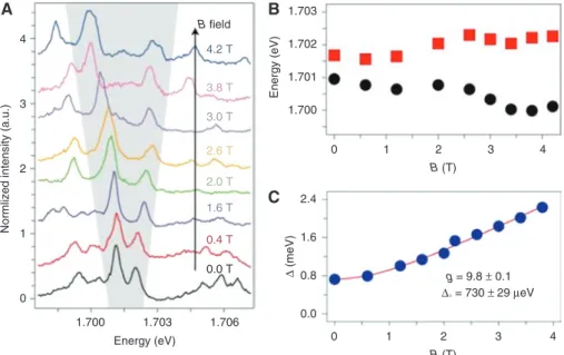
3 4 1.703 1.706 0.0 T 0.4 T 1.6 T 2.0 T 2.6 T 3.0 T 3.8 T 4.2 T 0 0.0 0.8 1.6 2.4 1.700 1.701 1.702 B field 1.703 Energy (eV) 1 2 3 g = 9.8 ± 0.1 ∆° = 730 ± 29 µeV B (T) ∆ (meV) 4 0 A B C 1 2 3 B (T) 4 Energy (eV)
Figure 2: Zeeman effect.
(A) Magnetic field dependence of emission spectra from an exemplary quantum emitter in WSe2 in the Faraday configuration. The gray
shading identifies the studied emitter. (B) Spectral location of two emission peaks associated with the emitter. (C) Spectral separation of the emission peaks (blue circles) as a function of magnetic field fitted with a hyperbolic function (red curve). Reproduced with permission from Ref. [8], Nature Publishing Group.
laser spectroscopy has been shown to further reduce the value of g2(0) to 0.02 [22]. Their excited state lifetime was
measured to be of the order of a few nanoseconds, three orders of magnitude higher than the delocalized excitons. Recently, much longer lifetimes (>200 ns) were reported in
defects in chemical vapor deposition (CVD)-grown WSe2
that are encapsulated by hBN [25]. The PL intensity also exhibited saturation with increasing power, as expected for an atom-like emitter. The zero-phonon line (ZPL) con-sists of at least 60% of the emission [22].
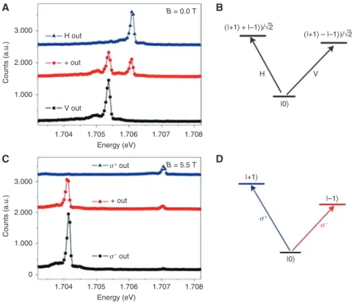
Highly resolved PL spectra revealed a doublet-like feature in their emission spectra. This is believed to be its fine-structure splitting (FSS) from the anisotropic electron-hole exchange interaction due to an asymmet-ric confinement potential of the single trapped exciton [5–8]. The magnitude of the FSS ranged between 600 and 900 μeV with nearly orthogonal polarization between the two peaks of the doublet [6]. This is illustrated by the energy level diagram with linearly polarized optical selection rules at zero magnetic field (Figure 3B). The application of a magnetic field in Faraday geometry led to a strong splitting of the doublets exhibiting the Zeeman effect with a g-factor ranging between ~5 and
13 [5, 6, 8, 26]. Figure 2A presents the increase in the splitting of an exemplary doublet as a function of the applied magnetic field. The magnetic field-dependent Zeeman splitting was fit to a hyperbolic dispersion func-tion (Figure 2B). At higher magnetic field, Zeeman energy also superseded the exchange energy, leading to the restoration of the circularly polarized emission from the doublets (Figure 3C and D). The change of the degree of circular polarization with magnetic field has not been studied in detail yet, which could further shed some light about the symmetry of quantum emitters [27]. On apply-ing a magnetic field parallel to the direction of the flake, no splitting was observed. The anisotropic behavior with the magnetic field direction is also observed in the case of delocalized excitons and is attributed to the fact that the orbital magnetic moment of a 2D material will point in the out-of-plane direction and will thus only couple to the magnetic field in the out-of-plane direction. This striking similarity with the delocalized excitons showed that 2D quantum emitters can inherit the optical valley selection rules from the delocalized exciton [5]. This demonstrated a promise in using the valley degree of freedom as an information carrier in these quantum emitters as well.
1.708 H V |0〉 |0〉 (|+1〉 + |–1〉)/√2– |+1〉 |–1〉 (|+1〉 – |–1〉)/√2– 1.707 Energy (eV) 1.706 1.705 V out + out H out 1.704 1.708 1.707 Energy (eV) σ– out σ– σ+ out σ+ + out B = 5.5 T B = 0.0 T Counts (a.u.) 1.706 1.705 1.704 0 1.000 2.000 3.000 Counts (a.u.) 1.000 2.000 3.000 A B C D
Figure 3: Polarization-resolved photoluminescence.
(A) Polarization-resolved PL spectra of an exemplary quantum emitter in WSe2 at zero magnetic field showing a cross-linearly polarized
doublet. (B) Zero-field energy-level diagram with linearly polarized optical selection rules. (C) At a magnetic field of 5.5 T, the doublet becomes cross-circularly polarized. (D) Its energy-level diagram. H, V, σ+, σ−, and + denote the horizontal, vertical, left-circular,
Although below the bandgap a spectrally narrow
emission was observed in other TMDCs such as MoSe2,
antibunching was only confirmed in WSe2 and WS2,
raising the question if quantum emitters are only limited to tungsten-based compounds. Moreover, the g-factor of localized emitters in tungsten-based compounds strongly matches the g-factor of the lowest lying dark exciton state in W-based compounds [26, 28–30], whereas the g-factor of the localized emitters in MoSe2 (~4) matches their lowest lying bright exciton state [31]. This observation also raises the question if these single excitons are trapped dark exci-tons in W-based compounds, which could, in fact, be also
related to the reason behind the large g-factor of WSe2
emitters (g ~ 5–13) compared to the bright exciton (g ~ 4). Time-dependent spectral wandering due to random charge and/or electric field fluctuations in the neigh-bourhood of the emitter are an issue for most solid-state quantum emitters and are also observed for the single-photon emitters in 2D materials. For example, charge fluctuation in the environment leads to the broadening of the linewidth of emitters in TMDC to several meVs [5, 8]. Even in quantum emitters hosted by insulating 2D mate-rials such as hBN, a photon coherence time of 81 ps was measured, which is less than the lifetime limited value due to the ultrafast spectral wandering in these emitters [32]. However, using different substrates such as Al2O3 [33] or GaInP [34, 35] has improved the quality and reduced the random spectral fluctuations of quantum emitters in both insulating [~45 μeV full width at half-maximum (FWHM) with nonresonant excitation] and semiconducting (70 μeV FWHM with nonresonant excitation) 2D materials. While resonant excitation was used to stabilize the ZPL for few tens of seconds [36], anti-Stokes excitation of quantum emitters in hBN was also used to suppress the spectral wandering [37]. Improving material quality [38] and/ or active electrical [39–41] or strain-based feedback can further help to minimize unwanted spectral wandering.
One of the major drawbacks of 2D quantum emitters was that they were only active at cryogenic temperatures. They demonstrated a nonlinear behavior with temperature
and their intensity strongly quenched above ~30 K [5, 8, 42]. Only recently, single-photon emission up to 160 K was achieved by a combination of nonradiative defect-free growth techniques and coupling to plasmonic nano-structures that increased the quantum yield to 44% with an activation energy of 92 meV [43]. This advance has led to a promise of using noncryogenic methods to activate these emitters. Furthermore, defect emission from bilayer
WS2 can survive up to 180 K [44]. Single-photon emitters
are also observed at room temperature [10] up to 800 K [45] from defects in hBN. Defect centers in hBN have the characteristics of an atomically sized defect center and at the same time share the advantages of a layered struc-ture, which sets an ultimate limit of miniaturization due to their atomic thickness and high mechanical robustness. The transition energy of the ZPL also varies over a large spectral range (1.6–2.5 eV) [46, 47]. The excited state energy of these emitters has also been extensively studied experi-mentally [10, 48] and theoretically from first-principles calculation [49–52]. A number of different defects in hBN were created in hBN using techniques, including electron/ ion irradiation [46, 53, 54], plasma treatment [55], laser ablation [56], controlled edge created via focused ion beam (FIB) milling [57], and strain engineering [58]. From first principles, it was inferred that the CBVN defect (substitu-tion of carbon in place of a boron atom and the opposite nitrogen atom is removed) is a potential emission source with a Huang-Rhys (HR) factor of 1.66, which is in good agreement with the experimental HR factor. The calculated PL line shape for this defect also reproduced a number of key features in the experimental PL lineshape [51]. Another density functional theory study elucidated the possibility of oxygen-related defects in hBN formed via plasma irra-diation [55]. Both carbon and oxygen are readily incorpo-rated in hBN during the growth process [51]. Owing to the 2D nature of the material, a combination of high-resolution atomic imaging combined with optical spectroscopy could be used to confirm the atomic origin of the defect [59].
At first, the promise of spin/valley manipulation upon the application of a magnetic field was only demonstrated
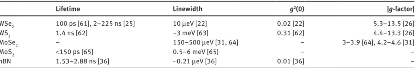
Table 1: Comparison of experimental values of emission lifetime, linewidth, g2(0), and g-factor values of localized emitters in different
monolayer materials.
Lifetime Linewidth g2(0) |g-factor|
WSe2 100 ps [61], 2–225 ns [25] 10 μeV [22] 0.02 [22] 5.3–13.5 [26]
WS2 1.4 ns [62] ~3 meV [63] 0.31 [62] 4.4–13.3 [26]
MoSe2 – 150–500 μeV [31, 64] – 3–3.9 [64], 4.2–4.6 [31]
MoS2 <150 ps [65] 0.5–6 meV [65] – –
by the emitters in WSe2 and WS2. No clear Zeeman effect was observed for the emitters in hBN. However, aniso-tropic PL pattern was recently observed upon the applica-tion of a magnetic field in hBN defects [60], suggesting the availability of optically addressable spin qubits [60] even in this platform. Table 1 presents a comparison of some of the physical parameters of different localized emitters in 2D materials.
3 Deterministic creation of
quantum traps
Scalability via the accurate positioning of quantum emit-ters has been one of the major challenges in quantum photonics. This requires designing emitters with identical properties that can be positioned at predetermined loca-tions on a chip. Single-photon emission from seemingly random locations in TMDCs and hBN made it challenging to locate and study these quantum emitters. Therefore, the natural strategy was to introduce artificial confinement
potentials in pristine materials using nanofabrication approaches. These include engineering the local strain, electrostatic field, and composition of the 2D material. Below we will describe some of the recent techniques used to achieve 3D localization in 2D materials.
3.1 Strain
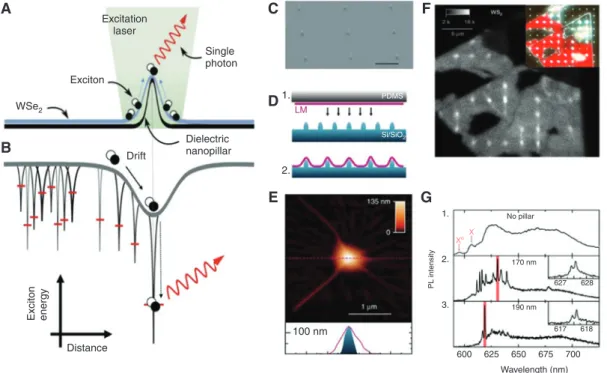
The large Young’s modulus and high elastic strain limit of 2D materials offer an interesting platform to strain engineer their optical and electronic properties. Several research groups [63, 66–68] used local strain engineering to demonstrate single exciton funneling (Figure 4A and B) in tungsten-based dichalcogenides that can create arrays of quantum emitters on the surface of 2D materials spaced a few microns apart. To create these arrays of emitters, a monolayer flake was transferred onto lithographically pat-terned nanopillars. Figure 4C presents a scanning electron micrograph (SEM) of an exemplary pillar array on a sub-strate and Figure 4D illusub-strates the transfer scheme. An atomic force microscopy (AFM) profile (Figure 4E) presents
Single photon Exciton Drift Distance 100 nm 600 3. 2. 1. 625 650 675 700 617 627 628 618 190 nm 170 nm PL intensity No pillar XoX ’ Wavelength (nm) Dielectric nanopillar 2. 1. PDMS Si/SiO2 LM Exciton energy WSe2 Excitation laser A B C D E F G
Figure 4: Deterministic generation of strain defined quantum emitters in 2D semiconductors.
(A and B) Schematic and band energy diagram of exciton funneling at a nanopillar. (C) SEM micrograph of the nanopillars. (D) Dry transfer technique of the TMDC on nanopillar. (E) AFM image of the TMDC over a nanopillar. (F) Integrated PL intensity raster scan of a 1L-WS2 flake
deposited on top of a 3 μm spaced, 170-nm-high nanopillar array, taken at 300 nW μm−2, 532 nm laser excitation at 10 K. The color-scale bar
maximum is 18 kcounts s−1. Inset, true-color dark-field micrograph of the same area. The red region corresponds to the WS
2 monolayer. (G) PL
spectra of 1L-WS2 at 10 K. Panel 1 shows a spectrum taken from a flat region away from nanopillars. Red arrows indicate unbound monolayer
neutral (X0) and charged (X−) excitons. Panels 2 and 3 show the representative spectra of WS
2 on 170 and 190 nm nanopillars, respectively.
Insets, high-resolution PL spectra of the red highlighted spectral regions, showing the FSS of the peaks. Reproduced with permission from Refs. [53, 54], Nature Publishing Group.
a tent-like appearance of the flake at the nanopillars with pleats emerging from the side of the nanopillars, creating highly strained points at the flake on the top of the pillar. The periodic strain via the nanopillars creates a periodic map of bandgap over the entire surface. The distinct gradi-ent and strain minima can be used to funnel a single exciton to the point of maximally applied strain through the nano-structure. An inhomogeneous distribution of 33 meV was observed from the different measured quantum emitters [66]. Palacios-Berraquero et al. [63] reported a red shift dis-tributed within 50 to 280 meV from the delocalized neutral exciton. They also observed an FSS over a range of 200 to 730 μeV and linewidths of ~180 μeV (Figure 4G), which are very similar to previously observed randomly distributed quantum emitters [5–8]. To study the influence of the local strain, the height of the nanopillars was varied. The net PL intensity was enhanced by increasing the height of the nan-opillar due to the enhanced funneling of the excitons. More-over, a higher aspect ratio pillar tended to produce a better yield of quantum emitters. A near-unity yield of quantum emitter (each pillar had at least one quantum emitter) was reported on the pillars having an aspect ratio of 0.3 and 0.52. Further, Palacios-Berraquero et al. [63] observed that increasing the nanopillar height reduces the spread in the number of peaks arising at each pillar. Spectral time traces of the emitters also displayed a strong dependence on the nanopillar height. Spectral wandering as low as 100 μeV was observed for pillar heights of 190 nm. For 60 nm pillar height, it increases to 2.5 meV. This technique was further extended to insulating hBN layers, which also presented deterministic activation of single-photon emitters in hBN at room temperature [58]. Excellent positioning accuracy with nanometer-scale resolution was also achieved recently by
nanoindentation using an AFM tip in a monolayer WSe2
placed on top of a deformable polymer that would retain the shape of the indentation [69]. This approach also increased the working temperature of the strain-defined emitters to 60 K. Even with this approach, no clear depend-ence of the emission energy could be derived from the indentation depth. However, the authors achieved nearly identical indentation shapes that would have more uniform strain profiles than dry transfer techniques on nanopillars that tend to create random pleats and folds in the flake from the nanopillar tip. Recently, such defect excitonic states in the presence of a nonuniform strain were also theoretically confirmed as the most likely candidate for quantum emit-ters in TMDCs [17]. The authors stated that weakly localized excitons are formed at the nonuniform strain gradient in the nanostructures. This strain forms a hybrid state with a localized point defect with broken valley symmetry that allows for radiative decay of the single hybrid exciton.
Simple point defects such as a single-Se or di-Se vacancy also fulfilled these criteria. Many other defects have been proposed as possible candidates [70–72], and as long as they satisfy the criteria of valley symmetry breaking, they can generate single photons as long as the localized state of the defect is energetically close enough to hybridize due to the strain.
3.2 Electrostatic traps
2D materials provide a novel approach toward engineering artificial lattices via van der Waals heterostructure where a small twist between two monolayers forms a periodic geo-metric lattice known as moiré pattern. The moiré pattern creates an array of nanoscale electrostatic potential that can trap quasiparticles including excitons. Four independ-ent groups [73–76] have reported the observation of optical emission from moiré-trapped excitons that confirm some of the theoretical predictions on moiré excitons [77] (see also Figure 5). The energy states and the periodicity of the superlattice can be controlled by the twist angle. Such modulation of the band structure has been also recognized previously, which lead to exotic transport properties such as correlated insulating states [78] and unconventional superconductivity [79]. If the variation in the band energy is sufficiently large and localized in space, a single exciton can get trapped in the moiré potential. Moiré excitons were possibly also generated while studying interlayer excitons in heterobilayers of TMDCs, but strong laser excitation would provide a broad background obscuring the observa-tion of the spectrally narrow emission from the moiré exci-tons. However, exploring the heterobilayer samples with different twist angles and lower excitation power revealed signatures of moiré-trapped excitons. Whereas all the four studies presented evidence of moiré excitons, Seyler et al. [73] demonstrated spectrally narrow emission from these twisted heterobilayers at low temperature (1.5 K) and low excitation power (approximately nanowatts). The emission spectra from these trapped excitons were highly circularly polarized (70%) and demonstrated a Zeeman effect under an applied magnetic field. The circular polarization proper-ties of the trapped interlayer excitons are distinct from those of the quantum emitters reported in monolayer TMDCs. The single-photon emitters in TMDC exhibit linearly polarized emission with a zero-field splitting known as the FSS due to anisotropic coulomb exchange interaction. Am FSS was not observed within the resolution of the measurement setup described by Seyler et al. This suggested that the confinement centers form at local atomic configurations
polarization, which is broken for strain/defect-induced quantum-confined exciton unless a magnetic field or doping is applied [5–8, 80, 81]. Furthermore, there is a dis-tribution in the g-factor for the strain-trapped exciton, but all trapped moiré excitons in similar stacking configuration have a similar g-factor. The extracted g-factor in Figure 6 is the same as the free interlayer excitons at the given twist angle. However, photon antibunching measurements will be necessary to confirm the quantum nature of the trapped moiré exciton. Apart from interlayer exciton trapping in moiré-based electrostatic potential, lateral electrostatic confinement can also be created using patterned gates in TMDC [15, 82] similar to III to V heterostructures [18]. A unique type II band alignment is predicted for gate-defined TMDC-based QDs [20]. 3D and 1D confinements of exci-tons were demonstrated in lithographically defined elec-trostatic traps in monolayer TMDC [82]. Moreover, lateral heterostructures between different 2D materials can also be grown to realize QD-like confinement potential [20, 83]. However, moiré potentials provide scalability via the seam-less generation of arrays of such confinement potential just by using different twist angles between stacked bilayers,
thus eliminating the need for time-consuming and costly nanofabrication. The periodicity of the moiré pattern can
be achieved up to ~10 nm in mixed MS2/MSe2 (M=Mo or W)
and can be increased up to ~100 nm in MoS2/WS2 or WSe2/ MoSe2 [77]. Furthermore, external strain can also be used to tune the moiré lattice constant. The absorption features associated with the moiré excitons were also tunable via an applied electric field [76]. Resolving individual interlayer excitons confined within a supercell using scanning probe optical spectroscopy would further establish the influence of a single moire confinement of excitons. However, a chal-lenge remains if the rotation of the materials toward an energetically favourable position can be controlled in such twisted bilayers. Furthermore, controlled CVD growth of 2D materials with predetermined twist angle will also be nec-essary for large-scale integration.
3.3 Direct manipulation at the atomic scale
One of the most revolutionary technologies in solid-state physics is the ability to manipulate individual atoms in a
1.3 + – x 1.30 0 10 20 30 A C B D –0.5 PL intensity 0 0.5 1.32 1.34 1.36 10 µW 0 5 10 1.4 1.5 1.6 Energy (eV) Energy Energy (eV) PL intensity (a.u. ) Energy (meV) ×130 θ ×7 20 nw θ = 20° θ = 2° PL intensity (a.u. ) 1.7
Figure 5: Exciton trapping by Moiré superlattice.
(A) Illustration of the moiré superlattice formed in a heterobilayer with twist angle θ. (B) Schematic of an exciton trapped in a moiré potential site. (C) Comparison of interlayer exciton PL from a heterobilayer with a 2° twist angle at excitation powers of 10 μW (dark red) and 20 nW (blue; intensity scaled by 7×). Inset, a Lorentzian fit to a representative PL peak indicates a linewidth of approximately 100 μeV (20 nW excitation power). (D) PL spectra from heterobilayers with twist angles of 2° (green) and 20° (blue; intensity scaled by 130×) at an excitation power of 5 μW. a.u., arbitrary units. Reproduced with permission from Ref. [73], Nature Publishing Group.
crystal. The previously used imaging techniques like scan-ning probe and electron microscopies can be reconfigured to not only provide atomic resolution imaging but also change the configuration of the crystal in the atomic scale.
Recently, an FIB was used to deterministically create edge defects in hBN resulting in single-photon emitters in hBN with 31% yield [57]. This approach created quantum emitters with an inhomogeneous distribution of the ZPL of ~350 meV similar to that observed in earlier studies. A low-pressure CVD method of producing large-scale hBN with possible preferential formation of one type of structural defect produced 86% of the emitters having ZPL within a ~74 meV bandwidth, the lowest spread reported so far in 2D material-based quantum emitters [84], which is almost an order of magnitude higher than that obtained for color centers in nanodiamond [85]. Whereas the former tech-nique offers nanometer-scale resolution of positioning
emitters, the latter offers a step forward in creating iden-tical emitters. Furthermore, each quantum emitter could have a slightly different local environment in the 2D lattice that could lead to the spectral inhomogeneity from the defects. In 2D materials, variation in local strain environ-ment can add to spectral inhomogeneity in addition to the variation in its local charge environment. Recently, Doppler-free spectroscopy in nitrogen-vacancy centers in diamond demonstrated that local magnetic fields are the main cause of the inhomogeneous broadening [86]. Such techniques could also be extended to hBN to determine the physical picture behind spectral inhomogeneity. To achieve a deterministically positioned source of indistin-guishable single-photon emitters in the 2D material plat-form, one could use a more localized probe approaching the atomic scale using techniques such as scanning tun-neling electron microscopy to generate identical defects.
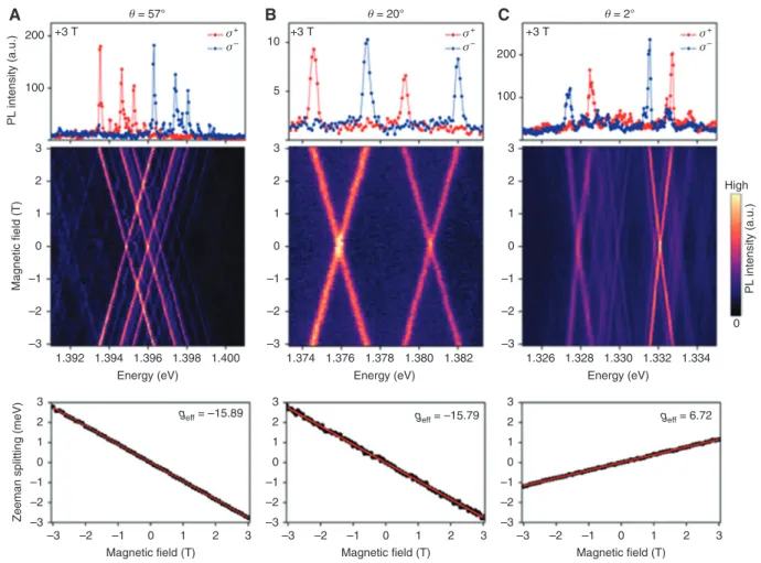
1.334 0 PL intensity (a.u.) PL intensity (a.u.) High Energy (eV) Energy (eV) Energy (eV) Magnetic field (T) 1.332 1.330 1.328 1.326 1.374 1.392 1.394 1.396 1.398 1.400 3 Magnetic field (T)
geff = –15.89 geff = –15.79 geff = 6.72
Zeeman splitting (meV)
2 1 0 –1 –2 –3 3 2 1 0 –1 –2 –3 3 100 200 A B C +3 T +3 T +3 T 2 1 0 –1 –2 –3 3 5 10 θ = 57° θ = 20° θ = 2° 100 200 2 1 0 –1 –2 –3 3 2 1 0 –1 –2 –3 3 2 1 0 –1 –2 –3 3 2 1 0 –1 –2 –3 3 Magnetic field (T) 2 1 0 –1 –2 –3 3 Magnetic field (T) 2 1 0 –1 –2 –3 1.376 1.378 1.380 1.382 σ– σ+ σ– σ+ σ– σ+
Figure 6: Zeeman effect of excitons trapped in moiré superlattice.
(A–C) Magnetic field-dependent PL from interlayer excitons in the MoSe2/WSe2 heterobilayer with twist angles of 57° (A), 20° (B), and 2° (C).
Top, helicity-resolved PL spectra at 3 T. The excitation is linearly polarized, and the σ+ and σ− components of the PL are shown in red and blue,
respectively. Middle, plot of total PL intensity as a function of magnetic field, showing a linear Zeeman shift of the σ+ and σ− polarized PL.
Bottom, Zeeman splitting of the polarization-resolved PL [Δ = Eσ+–Eσ−, where Eσ+ (Eσ−) is the peak energy of σ+ (σ−) polarized peak] as a function
of the applied magnetic field. The effective g-factors for the three samples (−15.89 ± 0.02, −15.79 ± 0.05, and 6.72 ± 0.02 for A–C, respectively) are extracted from a linear fit of Δ versus magnetic field (B; solid red line). Reproduced with permission from Ref. [73], Nature Publishing Group.
It has been demonstrated that a combination of electron irradiation and annealing results in the formation of a variety of defect centers in hBN [53]. Further, high-energy electron irradiation (~2 MeV) has also been demonstrated to increase single emitter concentration in a variety of hBN flakes without the need of annealing the flake [54]. Optimizing this to the atomic level using scanning trans-mission electron microscopy (STEM) could produce array of atom-like emitters in 2D materials. Further, a combina-tion of super-resolucombina-tion optical imaging [87, 88] together with STEM techniques can help in the complete character-ization of these emitters. A correlation between the local atomic configuration and their emission properties can address the intriguing question regarding the nature and origin of quantum emitters in 2D materials. Recent pro-gress has been made along these lines by demonstrating a correlation between PL and cathodoluminescence of sin-gle-photon emitters with local strain and crystallographic arrangement in hBN [89]. Several defects were found in a single diffraction-limited spot, which are believed to be the origin of the large spectral variability in the optical spectra instead of strain-induced variation in the ZPL. The probability of formation of these defects was much higher at multiple stacking-fault and fault dislocations, which was confirmed by high-resolution electron imaging. In
another study using Re-doped MoS2, a 3D scanning atomic
electron tomography was developed to map the spatial coordinates of each atom in the crystal with 4 pm resolu-tion. This technique was able to map the local strain of the crystal at the atomic level. This approach could also revolutionize ab initio calculations where experimental coordinates could be used as direct inputs for theoretical determination of the optical and electronic properties of the crystal [90]. Furthermore, this technique could also help quantify, resolve, and map the local strain in the quantum emitters in TMDC, which could not only help understand the atomic origin of these emitters but also help in engineering and scale these quantum emitters in the TMDC platform.
4 Integration with photonic
structures
A major step toward fully integrated quantum optics is the deterministic incorporation of high-quality single-photon sources in on-chip optical circuits. A lack of spatial control in QDs and color centers has impeded scalability with these systems [91–94]. Purcell enhancement is rather low in site-controlled QDs [95, 96] integrated with dielectric cavities;
however, nanoplasmonic cavity coupled quantum emit-ters [97, 98] present highly enhanced light-matter inter-action. Irrespective of plasmonic or dielectric photonic platforms, the 2D nature of the quantum emitters in 2D layered materials offer seamless incorporation of single-photon emitters into hybrid single-photonic structures for effi-cient light-matter interaction and integrated photonics. Because the emitters are not embedded in a dielectric host unlike most solid-state quantum emitters, a strong coupling efficiency can be achieved by coupling to near-field plasmonic structures as well as dielectric photonic components, opening the prospect of a strong light-matter interaction. This also strongly determines our ability of perfect extraction of single photons from this platform. In Section 2, we have seen that spatially controlled stress-ors such as lithographically defined nanostructures give us the ability to create single-photon emitters at any given location in the 2D material. Spontaneous emission enhancement was first presented in quantum emitters in
WSe2 generated from localized strain induced from the
surface roughness of a silver film that doubled as the active plasmonic material [61]. A single dipole emitter close to a plasmonic nanoparticle experiences a modified photonic mode density, leading to enhanced radiative decay rates and thus a spontaneous emission enhancement. Tem-porary stability and enhanced emission feature such as enhanced generation rate (lifetime down to hundreds of picoseconds from nanoseconds on silicon substrate) were demonstrated on a metallic surface than a dielectric. This approach was extended by other groups where an orderly grown array of plasmonic nanopillars were coupled with quantum emitters in 2D materials such as TMDC [99, 100] and hBN [101]. Recently, Luo et al. [99] conceived an approach that allowed to measure the same quantum emitter before and after coupling to a plasmonic cavity at 3.8 K. Coupling was achieved using the corners of a metal-lic nanocube that not only forms vertical plasmonic gap modes against a planar gold mirror but also acts as strain points for the autogeneration of a quantum emitter in the plasmonic gap cavity (Figure 7A–D). On the average, about four spectrally isolated emitters were found per site, further confirming the four corners of the nanocube that offers maximally localized strain on the transferred monolayer (Figure 7E). Antibunching data also confirmed the single-photon nature of the emitters (Figure 7G). An average g2(t = 0) value of 0.22 was obtained from all
studied emitters. A well-defined wavelength distribution of 35 nm facilitated matching their resonance with that of the designed nanocavity as the cavity resonance peak width is comparable to this distribution bandwidth (cavity
lifetimes of almost an order of magnitude was observed (Figure 7F) in the cavity coupled emitter, which was also accompanied by a commensurate increase in the PL inten-sity. Overall, Purcell factors of up to 551 and single-photon generation rate of 42 MHz with a linewidth of as low as
55 μeV were demonstrated for WSe2 emitters coupled to
plasmonic nanocavities [99]. Further, on using a flux
growth technique to synthesize WSe2, the quantum yield
of the emitters could also be increased from 1% to 65% on integration with these plasmonic nanocavities. With this demonstration, a directional outcoupling of the quantum light is also necessary for collection. The routing of single photons was successfully demonstrated in plasmonic [102, 103] as well as dielectric waveguide [104–106]. Statis-tical analysis of the position of different quantum emitters coupled to plasmonic waveguides showed that they are more likely to form close to the edges of the waveguides [103] with Purcell factor up to 15 ± 3, thus negating the need for pick and place. The coupling of single localized defects in a WSe2 monolayer was shown to self-align to the
surface plasmon mode of a silver nanowire, thus present-ing an average couplpresent-ing efficiency of 26 ± 11%. In general, QDs in nanophotonic waveguides also serve as a powerful platform for dramatically enhancing light-matter interac-tions. A QD in a photonic crystal waveguide can emit more than 98% of the emitted photons into the propagating mode of the waveguide [107]. QDs sitting in a nanobeam waveguide have also been demonstrated to emit single photons with high indistinguishability [108, 109], which is a key ingredient in quantum information processing [110]. Single photons from the 2D platform could also benefit from such integration.
5 Quantum light manipulation
Given that 2D material-based quantum emitters can be deterministically created and integrated with photonic components, a major outstanding question concerns if their emission properties can be controllably tuned via
10 100 1000 0 100 |E | 2/|E 0 | 2 |E | 2/|E 0 | 2 200 300 1 1 0 0 10 20 30 40 2 4 6 8 Emitters per site
Occurrenc e 0.1 1 10 2 3 Uncoupled Au mirror Au cube WSe2 Au mirror Sapphire wafer Coupled A B C E F G D T1 (ns) Fp (2) g (τ ) 4 5 6 7 8 9 10 11 12 –100 0.0 0.5 1.0 0 100 Time (ns) 200 0 1 2 0 100 200 300 Strain |εzz | (%) Quantum emitter
Figure 7: Quantum emitters coupled to plasmonic nanostructure.
(A) Schematic of monolayer WSe2 coupled to a plasmonic Au nanocube cavity array. The WSe2 is separated from the plasmonic Au cubes and the planar Au layer by a 2 nm Al2O3 spacer layer on each side to prevent optical quenching and short circuiting of the nanoplasmonic
gap mode (depicted by gray shading in the inset). The transparent sapphire wafer allows the optical addressing of the quantum emitters. (B) Side view of the simulated intensity enhancement (|E|2 / |E
0|2) distribution profile illustrating the confinement of the plasmon across the
vertical gap containing the WSe2. Scale bar, 50 nm. (C) Top view of simulated |E|2 / |E
0|2 showing four plasmonic hotspots at cube corners.
Scale bar, 100 nm. (D) Simulation of the strain profile induced in the WSe2 layer when stamped onto a nanocube, showing that the highest
strain occurs at cube corners coinciding with plasmonic hotspots. Scale bar, 100 nm. (E) Histogram of quantum emitter occurrence on the array, demonstrating the high success rate for creating four isolated quantum emitters per nanocube location. (F) Distribution of spontaneous emission lifetimes T1 times (left y-axis) recorded before (uncoupled) and after (coupled) closing the cavity. Diamonds represent the corresponding FP for each quantum emitter (right y-axis). (G) Second-order photon correlation function g2(τ) recorded under pulsed
external fields. The controlled manipulation of photonic and spin degrees of freedom of such quantum emitters could enable the generation of quantum entanglement across networks of such emitters, setting the bases of quantum technologies such as quantum repeater net-works. The first step along this direction was via a back-gated monolayer that presented a modulation of the intensity and lifetimes of the quantum emitters as a function of applied voltage [8]. The promise of electri-cally controlling the single-photon emitters in 2D mate-rials opened up many possibilities. Engineering van der Waals heterostructure with a wide range of unique atomically thin layers has been instrumental in revealing novel physical phenomenon as well as in the develop-ment of 2D material-based optoelectronic devices [74, 76, 79, 111, 112].
Figure 8A presents an exemplary device illustrating an assembled van der Waals heterostructure. Such devices were also used to demonstrate all electrical generation of quantum light from individual emitters in 2D materials [62, 114, 115]. This made the 2D quantum emitters among the very few single-photon sources that can be electrically activated [116–119]. Both vertical [62, 114, 115] and lateral [114] van der Waals heterostructures were assembled where a monolayer or bilayer TMDC was the active optical material hosting single emitters and graphene served as the source and drain and hBN as the dielectric spacer layers for engineered tunneling contacts. At low current densities and low temperatures (~5 K), spectrally narrow lines were observed in the electroluminescence from spa-tially localized regions in the monolayer semiconductor.
van der Waals heterostructure-based devices were also used to demonstrate the quantum-confined Stark effect in both localized [113, 115, 120] and delocalized excitons [121–123] in 2D materials. Both quadratic and linear Stark effects were observed from quantum emitters with a maximum energy control of ~21 meV. Further, a modula-tion of the FSS owing to electric field-induced change in the electron-hole wave-function of the confined exciton was observed, accompanied by a restoration of their cir-cular polarization [120]. Stark effect-based modulation at room temperature was also observed in hBN defects along with a modulation of the fluorescence lifetimes [84, 124–128]. A maximum Stark shift of 48 meV was observed for hBN defects in an ionic liquid device [84], which, however, is not quite as high as the inhomogeneous dis-tribution of the spectral frequencies but does exceed the typical resonance linewidths of most optical resonators and hence can be used for strong coupling. Apart from electrical control, external parameters such as pressure (15 meV/GPa) [129] and strain (6 meV/%) [130] have also been used to control the optical properties of these active defects in hBN.
Engineering coherent quantum-confined single-spin states for single and two qubit operations has also been proposed using 2D material-based QDs [20, 131–134]. The bulk valley and spin optical selection rules can be inher-ited in different forms by 2D TMDC-based quantum emit-ters, allowing the definition of spin-valley qubit with desired optical and electrical controllability [20, 132, 135– 137]. Various experimental efforts have also been demon-strated in electrically charging the quantum emitters with
100 0 200 Energy (eV) 300 1.611 –20 –40 –60 1.616 1.621 D1 S1 D2 10 meV ∆E = 21 meV µ = –2.4 D Field (MV/m) V –100 1.670 1.680 FLG h-BN WSe2 1.690 A B C Energy (meV) Gate voltage (V)
Figure 8: Voltage controlled emission.
(A) Illustration of a van der Waals heterostructure device used for the electrical manipulation of quantum emitters in 2D materials. (B) Stark effect of a typical quantum emitter in a van der Waals heterostructure exhibiting a spectral shift of 21 meV. (C) PL intensity maps as a function of electrostatic doping via a gate voltage (Vg) from a typical QD in WSe2. S1 and D1 have correlated spectral jittering patterns (highlighted by
solid symbols) and the same turn-on voltage (dashed line), respectively. As a result, they are assigned to the same QD groups. The energy spacing between the S- and D-peaks is about 10 meV for all QDs. S1 corresponds to a single charged exciton and D1 corresponds to a single neutral exciton. Reproduced with permission from Ref. [113], American Chemical Society (A and B) and Ref. [81], Nature Publishing Group (C).
a single electron or hole, marking a first important step in the realization of a 2D material-based qubit [80, 81, 138]. Electrostatically doped monolayer was used to demo-nstrate both positively [81] and negatively [80] charged single trion. A tunnel coupling device with a tunable Fermi reservoir demonstrated the formation of both negatively and positively charged trions in localized emitters [138]. Both positive [80, 138] and negative binding [81] energies of these confined trions were demonstrated. A negative binding energy due to the different confining potential for electron and holes was also reported in InGaAs QD [139]. Furthermore, the electron-hole exchange interac-tion responsible for valley mixing is reduced in singly charged QDs, leading to the recovery of valley polarization and enabling optical initialization and read out of its spin valley [80, 81]. The spin or valley degree of freedom of this single charge in a QD can be used to store information or perform calculations through optical control [140, 141]. The valley polarization selection rules inherited by the local-ized trions provide a pathway toward realizing a locallocal-ized spin-valley-photon interface. In the future, theoretical models and experimental techniques should be explored to allow the rotation of an electron spin/valley state into a superposition of up and down or K and K′, the measure-ment of the quantum state of an individual spin, and the coherent control of the interaction between two neighbor-ing spins [18]. The lifetime after initialization, relaxation, and dephasing mechanisms for the spin/valley state of 2D quantum emitters also need to be studied in detail to deter-mine their suitability for practical applications.
6 Conclusion
In conclusion, many different types of quantum emitters have been discovered in recent years with exceptional properties including high brightness, high internal effi-ciency, spectral tunability, and first signatures of quantum interfaces to spin quantum memories. They raise the pros-pect of atomic-scale control, and they are promising for efficient integration with electronic and optical circuits. Recent experimental and theoretical research is begin-ning to elucidate their atomic structure and optoelectronic properties, as the study of these localized emitters is still in its experimental infancy. A focus on the following issues should give valuable basic scientific insights into these emitters and their mesoscopic quantum environment while also illuminating the path toward practical applications in emerging quantum technologies: understanding disorder and decoherence to drive toward Fourier transform-limited linewidth in quantum emitters hosted by insulating [142]
and semiconducting 2D materials, ideally at room tempera-ture; unraveling the origin of the emission for designing stable spin-valley-photon interface at the single-photon level [143]; the development of fabrication and spectro-scopy methods at the atomic scale; and the development of techniques to seamlessly integrate and scale quantum emitters with well-controlled spectral and spin properties into electro-optic devices and systems. For single-photon emitters specifically in TMDCs, engineering a stronger strain could improve quantum yield (2D materials can be stretched up to 10% [144]; the present applied strain is up to 2% [145]) and increase their operating temperature. It could also be interesting to study the differences in W- and Mo-based 2D semiconductors that led to the confirma-tion of antibunched photon emission only in the former type of TMDC [31, 64]. Generating single-photon emitters in different 2D materials can likely cover wide spectral ranges. Investigating quantum emitter candidate systems with long-lived spin states could open new applications in quantum sensing possibly to offer a better alternative, in some instances, to systems such as the nitrogen-vacancy center in diamond and in quantum repeaters. This is also of considerable interest in the field of optomechanics as 2D materials can be used for sensing weak forces and small dis-placements because of their low mass and mechanical res-onances with high Q-factor [146–149]. Further, high-speed quantum state transfer between a microwave photon, a phonon, and an optical photon has also been proposed by coupling the optical vibration of a mechanical 2D resonator with a single-photon emitter in its host that could be tuned by Stark effect or strain [150]. Quantum emitters in 2D mate-rials may couple to mechanical vibration of the membrane via vacuum dispersive forces [151]. Furthermore, interfac-ing hybrid quantum systems via distributed or on-chip photonic channels have also been proposed as the widely spectrally tunable emission of 2D quantum emitters would facilitate spectral matching to quantum memories such as Rb atoms or diamond SiV centers [62].
Funding: D.E. acknowledges partial support from Army Research Office (ARO) Multidisciplinary Uni-versity Research Initiative (MURI) program, grant no. W911NF-18-1-0431. N.V. acknowledges support from air force office of Scientific Research, grant number AFOSR FA9550-19-1-0074.
References
[1] Mak KF, Shan J. Photonics and optoelectronics of 2D semi-conductor transition metal dichalcogenides. Nat Photonics 2016;10:216–26.
[2] Liu X, Galfsky T, Sun Z, et al. Strong light-matter coupling in two-dimensional atomic crystals. Nat Photonics 2014;9:30. [3] Wu S, Buckley S, Schaibley JR, et al. Monolayer
semicon-ductor nanocavity lasers with ultralow thresholds. Nature 2015;520:69–72.
[4] Dhara S, Chakraborty C, Goodfellow KM, et al. Anomalous dis-persion of microcavity trion-polaritons. Nat Phys 2017;14:130. [5] Srivastava A, Sidler M, Allain AV, Lembke DS, Kis A, Imamoğlu A. Optically active quantum dots in monolayer WSe2. Nat
Nano-technol 2015;10:491–6.
[6] He Y-M, Clark G, Schaibley JR, et al. Single quantum emitters in monolayer semiconductors. Nat Nanotechnol 2015;10:497–502. [7] Koperski M, Nogajewski K, Arora A, et al. Single photon
emitters in exfoliated WSe2 structures. Nat Nanotechnol
2015;10:503–6.
[8] Chakraborty C, Kinnischtzke L, Goodfellow KM, Beams R, Vami-vakas AN. Voltage-controlled quantum light from an atomically thin semiconductor. Nat Nanotechnol 2015;10:507–11. [9] Tonndorf P, Schmidt R, Schneider R, et al. Single-photon
emis-sion from localized excitons in an atomically thin semiconduc-tor. Optica 2015;2:347–52.
[10] Tran TT, Bray K, Ford MJ, Toth M, Aharonovich I. Quantum emis-sion from hexagonal boron nitride monolayers. Nat Nanotech-nol 2016;11:37–41.
[11] Awschalom DD, Hanson R, Wrachtrup J, Zhou BB. Quantum technologies with optically interfaced solid-state spins. Nat Photonics 2018;12:516–27.
[12] Atatüre M, Englund D, Vamivakas N, Lee S-Y, Wrachtrup J. Mate-rial platforms for spin-based photonic quantum technologies. Nat Rev Mater 2018;3:38–51.
[13] Gao WB, Imamoglu A, Bernien H, Hanson R. Coherent manipu-lation, measurement and entanglement of individual solid-state spins using optical fields. Nat Photonics 2015;9:363. [14] Li X, Rui M, Song J, Shen Z, Zeng H. Carbon and graphene
quan-tum dots for optoelectronic and energy devices: a review. Adv Funct Mater 2015;25:4929–47.
[15] Song X-X, Liu D, Mosallanejad V, et al. A gate defined quantum dot on the two-dimensional transition metal dichalcogenide semiconductor WSe2. Nanoscale 2015;7:16867–73.
[16] Brooks M, Burkard G. Theory of strain-induced confinement in transition metal dichalcogenide monolayers. Phys Rev B Condens Matter 2018;97:195454.
[17] Linhart L, Paur M, Smejkal V, Burgdörfer J, Mueller T, Libisch F. Localized inter-valley defect excitons as single-photon emitters in WSe2. arXiv preprint arXiv:1904 03217. 2019. Available at:
https://arxiv.org/abs/1904.03217.
[18] Hanson R, Kouwenhoven LP, Petta JR, Tarucha S, Vandersypen LMK. Spins in few-electron quantum dots. Rev Mod Phys 2007;79:1217–65.
[19] Ciorga M, Sachrajda AS, Hawrylak P, et al. Addition spectrum of a lateral dot from coulomb and spin-blockade spectroscopy. Phys Rev B Condens Matter 2000;61:R16315–8.
[20] Liu G-B, Pang H, Yao Y, Yao W. Intervalley coupling by quantum dot confinement potentials in monolayer transition metal dichalcogenides. N J Phys 2014;16:105011.
[21] Mak KF, Lee C, Hone J, Shan J, Heinz TF. Atomically thin MoS2: a new direct-gap semiconductor. Phys Rev Lett
2010;105:136805.
[22] Kumar S, Brotóns-Gisbert M, Al-Khuzheyri R, et al. Resonant laser spectroscopy of localized excitons in monolayer WSe2.
Optica 2016;3:882–6.
[23] Shepard GD, Ajayi OA, Li X, Zhu X-Y, Hone J, Strauf S. Nano-bubble induced formation of quantum emitters in monolayer semiconductors. 2D Mater 2017;4:021019.
[24] Zheng YJ, Chen Y, Huang YL, et al. Point defects and localized excitons in 2D WSe2. ACS Nano 2019;13:6050–9.
[25] Dass CK, Khan MA, Clark G, et al. Ultra-long lifetimes of single quantum emitters in monolayer WSe2/hBN heterostructures.
Adv Quant Technol 2019;4:1900022.
[26] Koperski M, Molas MR, Arora A, et al. Orbital, spin and valley contributions to Zeeman splitting of excitonic resonances in MoSe2, WSe2 and WS2 Monolayers. 2D Mater 2018;6:015001.
[27] Bayer M, Ortner G, Stern O, et al. Fine structure of neutral and charged excitons in self-assembled In(Ga)As/(Al)GaAs quan-tum dots. Phys Rev B Condens Matter 2002;65:195315. [28] Li Z, Wang T, Jin C, et al. Emerging photoluminescence from the
dark-exciton phonon replica in monolayer WSe2. Nat Commun
2019;10:2469.
[29] Zhou Y, Scuri G, Wild DS, et al. Probing dark excitons in atomi-cally thin semiconductors via near-field coupling to surface plasmon polaritons. Nat Nanotechnol 2017;12:856–60. [30] Zhang X-X, You Y, Zhao SYF, Heinz TF. Experimental
evi-dence for dark excitons in monolayer WSe2. Phys Rev Lett
2015;115:257403.
[31] Chakraborty C, Goodfellow KM, Nick Vamivakas A. Localized emission from defects in MoSe2 layers. Opt Mater Express
2016;6:2081–7.
[32] Sontheimer B, Braun M, Nikolay N, Sadzak N, Aharonovich I, Benson O. Photodynamics of quantum emitters in hexagonal boron nitride revealed by low-temperature spectroscopy. Phys Rev B Condens Matter 2017;96:121202.
[33] Li X, Shepard GD, Cupo A, et al. Nonmagnetic quantum emitters in boron nitride with ultranarrow and sideband-free emission spectra. ACS Nano 2017;11:6652–60.
[34] Iff O, He Y-M, Lundt N, et al. Substrate engineering for high-quality emission of free and localized excitons from atomic monolayers in hybrid architectures. Optica 2017;4:669–73. [35] He Y-M, Iff O, Lundt N, et al. Cascaded emission of single
photons from the biexciton in monolayered WSe2. Nat Commun
2016;7:13409.
[36] Dietrich A, Bürk M, Steiger ES, et al. Observation of Fourier transform limited lines in hexagonal boron nitride. Phys Rev B Condens Matter 2018;98:081414.
[37] Tran TT, Bradac C, Solntsev AS, Toth M, Aharonovich I. Suppres-sion of spectral diffuSuppres-sion by anti-Stokes excitation of quantum emitters in hexagonal boron nitride [Internet]. arXiv [physics. optics]. 2019. Available at: http://arxiv.org/abs/1902.03711. [38] Greentree AD, Olivero P, Draganski M, et al. Critical
compo-nents for diamond-based quantum coherent devices. J Phys Condens Matter 2006;18:S825.
[39] Schmidgall ER, Chakravarthi S, Gould M, et al. Frequency con-trol of single quantum emitters in integrated photonic circuits. Nano Lett 2018;18:1175–9.
[40] Acosta VM, Santori C, Faraon A, et al. Dynamic stabilization of the optical resonances of single nitrogen-vacancy centers in diamond. Phys Rev Lett 2012;108:206401.
[41] Hansom J, Schulte CHH, Matthiesen C, Stanley MJ, Atatüre M. Frequency stabilization of the zero-phonon line of a quan-tum dot via phonon-assisted active feedback. Appl Phys Lett 2014;105:172107.
[42] He Y-M, Höfling S, Schneider C. Phonon induced line broadening and population of the dark exciton in a deeply
trapped localized emitter in monolayer WSe2. Opt Express
2016;24:8066–73.
[43] Luo Y, Liu N, Hone JC, Strauf S. Single photon emission in WSe2 up 160 K by quantum yield control [Internet]. arXiv
[cond-mat.mtrl-sci]. 2019. Available at: http://arxiv.org/ abs/1903.00126.
[44] Tan Q-H, Ren S-L, Shen T, et al. Unraveling the defect emission and exciton-lattice interaction in bilayer WS2. J Phys Chem C
2019;123:4433–40.
[45] Kianinia M, Regan B, Tawfik SA, et al. Robust solid-state quantum system operating at 800 K. ACS Photonics 2017;4:768–73. [46] Tran TT, Elbadawi C, Totonjian D, et al. Robust multicolor single
photon emission from point defects in hexagonal boron nitride. ACS Nano 2016;10:7331–8.
[47] Wigger D, Schmidt R, Del Pozo-Zamudio O, et al. Phonon-assisted emission and absorption of individual color centers in hexagonal boron nitride. 2D Mater 2019;6:035006.
[48] Jungwirth NR, Fuchs GD. Optical absorption and emission mechanisms of single defects in hexagonal boron nitride. Phys Rev Lett 2017;119:057401.
[49] Abdi M, Chou J-P, Gali A, Plenio MB. Color centers in hexagonal boron nitride monolayers: a group theory and ab initio analy-sis. ACS Photonics 2018;5:1967–76.
[50] Grinyaev SN, Konusov FV, Lopatin VV. Deep levels of nitrogen vacancy complexes in graphite-like boron nitride. Phys Solid State 2002;44:286–93.
[51] Tawfik SA, Ali S, Fronzi M, et al. First-principles investigation of quantum emission from hBN defects. Nanoscale 2017;9: 13575–82.
[52] Wu F, Galatas A, Sundararaman R, Rocca D, Ping Y. First-principles engineering of charged defects for two-dimensional quantum technologies. Phys Rev Mater 2017;1:071001. [53] Exarhos AL, Hopper DA, Grote RR, Alkauskas A, Bassett LC.
Optical signatures of quantum emitters in suspended hexago-nal boron nitride. ACS Nano 2017;11:3328–36.
[54] Ngoc My Duong H, Nguyen MAP, Kianinia M, et al. Effects of high-energy electron irradiation on quantum emitters in hexagonal boron nitride. ACS Appl Mater Interfaces 2018;10:24886–91. [55] Xu Z-Q, Elbadawi C, Tran TT, et al. Single photon emission
from plasma treated 2D hexagonal boron nitride. Nanoscale 2018;10:7957–65.
[56] Hou S, Birowosuto MD, Umar S, et al. Localized emission from laser-irradiated defects in 2D hexagonal boron nitride. 2D Mater 2017;5:015010.
[57] Ziegler J, Klaiss R, Blaikie A, Miller D, Horowitz VR, Alemán BJ. Deterministic quantum emitter formation in hexagonal boron nitride via controlled edge creation. Nano Lett 2019;19:2121–7. [58] Proscia NV, Shotan Z, Jayakumar H, et al. Near-deterministic
activation of room-temperature quantum emitters in hexagonal boron nitride. Optica 2018;5:1128–34.
[59] Dyck O, Ziatdinov M, Lingerfelt DB, et al. Atom-by-atom fabrication with electron beams. Nat Rev Mater 2018;30:e1707281.
[60] Exarhos AL, Hopper DA, Patel RN, Doherty MW, Bassett LC. Magnetic-field-dependent quantum emission in hexagonal boron nitride at room temperature. Nat Commun 2019;10:222. [61] Tripathi LN, Iff O, Betzold S, et al. Spontaneous emission
enhancement in strain-induced WSe2 monolayer-based
quantum light sources on metallic surfaces. ACS Photonics 2018;5:1919–26.
[62] Palacios-Berraquero C, Barbone M, Kara DM, et al. Atomi-cally thin quantum light-emitting diodes. Nat Commun 2016;7:12978.
[63] Palacios-Berraquero C, Kara DM, Montblanch AR-P, et al. Large-scale quantum-emitter arrays in atomically thin semiconduc-tors. Nat Commun 2017;8:15093.
[64] Branny A, Wang G, Kumar S, et al. Discrete quantum dot like emitters in monolayer MoSe2: spatial mapping,
magneto-optics, and charge tuning. Appl Phys Lett 2016;108:142101. [65] Klein J, Lorke M, Florian M, et al. Atomistic defect states
as quantum emitters in monolayer MoS2 [Internet]. arXiv
[cond-mat.mes-hall]. 2019. Available at: http://arxiv.org/ abs/1901.01042.
[66] Branny A, Kumar S, Proux R, Gerardot BD. Deterministic strain-induced arrays of quantum emitters in a two-dimensional semiconductor. Nat Commun 2017;8:15053.
[67] Kumar S, Kaczmarczyk A, Gerardot BD. Strain-induced spatial and spectral isolation of quantum emitters in mono- and bilayer WSe2. Nano Lett 2015;15:7567–73.
[68] Kern J, Niehues I, Tonndorf P, et al. Nanoscale positioning of single-photon emitters in atomically thin WSe2. Adv Mater
2016;28:7101–5.
[69] Rosenberger MR, Dass CK, Chuang H-J, et al. Quantum cal-ligraphy: writing single-photon emitters in a two-dimensional materials platform. ACS Nano 2019;13:904–12.
[70] Zhang S, Wang C-G, Li M-Y, et al. Defect structure of localized excitons in a WSe2 monolayer. Phys Rev Lett 2017;119:046101.
[71] Zheng YJ, Chen Y, Huang YL, et al. The origin of single photon emission in 2D WSe2 [Internet]. arXiv [cond-mat.mtrl-sci]. 2018.
Available at: http://arxiv.org/abs/1811.00221.
[72] Zheng YJ, Quek SY. First principles study of intrinsic and extrin-sic point defects in monolayer WSe2 [Internet]. arXiv [cond-mat.
mtrl-sci]. 2019. Available at: http://arxiv.org/abs/1901.05238. [73] Seyler KL, Rivera P, Yu H, et al. Signatures of moiré-trapped
valley excitons in MoSe2/WSe2 heterobilayers. Nature
2019;567:66–70.
[74] Alexeev EM, Ruiz-Tijerina DA, Danovich M, et al. Resonantly hybridized excitons in moiré superlattices in van der Waals heterostructures. Nature 2019;567:81–6.
[75] Tran K, Moody G, Wu F, et al. Evidence for moiré excitons in van der Waals heterostructures. Nature 2019;567:71–5.
[76] Jin C, Regan EC, Yan A, et al. Observation of moiré excitons in WSe2/WS2 heterostructure superlattices. Nature 2019;567:
76–80.
[77] Yu H, Liu G-B, Tang J, Xu X, Yao W. Moiré excitons: from programmable quantum emitter arrays to spin-orbit-coupled artificial lattices. Sci Adv 2017;3:e1701696.
[78] Kim K, DaSilva A, Huang S, et al. Tunable moiré bands and strong correlations in small-twist-angle bilayer graphene. Proc Natl Acad Sci U S A 2017;114:3364–9.
[79] Cao Y, Fatemi V, Fang S, et al. Unconventional superconductiv-ity in magic-angle graphene superlattices. Nature 2018;556: 43–50.
[80] Chakraborty C, Qiu L, Konthasinghe K, Mukherjee A, Dhara S, Vamivakas N. 3D localized trions in monolayer WSe2 in
a charge tunable van der Waals heterostructure. Nano Lett 2018;18:2859–63.
[81] Lu X, Chen X, Dubey S, et al. Optical initialization of a single spin-valley in charged WSe2 quantum dots. Nat Nanotechnol
[82] Wang K, De Greve K, Jauregui LA, et al. Electrical control of charged carriers and excitons in atomically thin materials. Nat Nanotechnol 2018;13:128–32.
[83] Huang C, Wu S, Sanchez AM, et al. Lateral heterojunctions within monolayer MoSe2-WSe2 semiconductors. Nat Mater
2014;13:1096–101.
[84] Mendelson N, Xu Z-Q, Tran TT, et al. Engineering and tuning of quantum emitters in few-layer hexagonal boron nitride. ACS Nano 2019;13:3132–40.
[85] Jantzen U, Kurz AB, Rudnicki DS, et al. Nanodiamonds carry-ing silicon-vacancy quantum emitters with almost lifetime-limited linewidths. N J Phys 2016;18:073036.
[86] Rosenzweig Y, Schlussel Y, Folman R. Probing the origins of inhomogeneous broadening in nitrogen-vacancy centers with Doppler-free-type spectroscopy. Phys Rev B Condens Matter 2018;98:014112.
[87] Feng J, Deschout H, Caneva S, et al. Imaging of optically active defects with nanometer resolution. Nano Lett 2018;18: 1739–44.
[88] Kianinia M, Bradac C, Sontheimer B, et al. All-optical control and super-resolution imaging of quantum emitters in layered materials. Nat Commun 2018;9:874.
[89] Hayee F, Yu L, Zhang JL, et al. Correlated optical and electron microscopy reveal the role of multiple defect species and local strain on quantum emission [Internet]. arXiv [cond-mat.mtrl-sci]. 2019. Available at: http://arxiv.org/abs/1901.05952. [90] Tian X, Kim DS, Yang S, et al. Correlating 3D atomic defects
and electronic properties of 2D materials with picom-eter precision. Available at: https://arxiv.org/ftp/arxiv/ papers/1901/1901.00633.pdf.
[91] Aharonovich I, Englund D, Toth M. Solid-state single-photon emitters. Nat Photonics 2016;10:631.
[92] Senellart P, Solomon G, White A. High-performance semicon-ductor quantum-dot single-photon sources. Nat Nanotechnol 2017;12:1026–39.
[93] Zhang JL, Sun S, Burek MJ, et al. Strongly cavity-enhanced spontaneous emission from silicon-vacancy centers in dia-mond. Nano Lett 2018;18:1360–5.
[94] Riedel D, Söllner I, Shields BJ, et al. Deterministic enhance-ment of coherent photon generation from a nitrogen-vacancy center in ultrapure diamond. Phys Rev X 2017;7:031040. [95] Kaganskiy A, Gericke F, Heuser T, Heindel T, Porte X,
Reitzen-stein S. Micropillars with a controlled number of site-con-trolled quantum dots. Appl Phys Lett 2018;112:071101. [96] Schneider C, Heindel T, Huggenberger A, et al. Single photon
emission from a site-controlled quantum dot-micropillar cav-ity system. Appl Phys Lett 2009;94:111111.
[97] Russell KJ, Liu T-L, Cui S, Hu EL. Large spontaneous emis-sion enhancement in plasmonic nanocavities. Nat Photonics 2012;6:459.
[98] Akselrod GM, Argyropoulos C, Hoang TB, et al. Probing the mechanisms of large Purcell enhancement in plasmonic nano-antennas. Nat Photonics 2014;8:835.
[99] Luo Y, Shepard GD, Ardelean JV, et al. Deterministic coupling of site-controlled quantum emitters in monolayer WSe2 to
plasmonic nanocavities. Nat Nanotechnol 2018;13:1137–42. [100] Cai T, Kim J-H, Yang Z, Dutta S, Aghaeimeibodi S, Waks E.
Radiative enhancement of single quantum emitters in WSe2
monolayers using site-controlled metallic nanopillars. ACS Photonics 2018;5:3466–71.
[101] Tran TT, Wang D, Xu Z-Q, et al. Deterministic coupling of quan-tum emitters in 2D materials to plasmonic nanocavity arrays. Nano Lett 2017;17:2634–9.
[102] Cai T, Dutta S, Aghaeimeibodi S, et al. Coupling emission from single localized defects in two-dimensional semiconductor to surface plasmon polaritons. Nano Lett 2017;17:6564–8. [103] Blauth M, Jürgensen M, Vest G, et al. Coupling single
photons from discrete quantum emitters in WSe2 to
lithographically defined plasmonic slot waveguides. Nano Lett 2018;18:6812–9.
[104] Peyskens F, Chakraborty C, Muneeb M, Van Thourhout D, Englund D. Integration of single photon emitters in 2D layered materials with a silicon nitride photonic chip [Internet]. arXiv [physics.optics]. 2019. Available at: http://arxiv.org/ abs/1904.08841.
[105] White D, Branny A, Chapman RJ, et al. Atomically-thin quantum dots integrated with lithium niobate photonic chips [Invited]. Opt Mater Express 2019;9:441–8.
[106] Tonndorf P, Del Pozo-Zamudio O, Gruhler N, et al. On-chip waveguide coupling of a layered semiconductor single-photon source. Nano Lett 2017;17:5446–51.
[107] Arcari M, Söllner I, Javadi A, et al. Near-unity coupling effi-ciency of a quantum emitter to a photonic crystal waveguide. Phys Rev Lett 2014;113:093603.
[108] Kiršanskė G, Thyrrestrup H, Daveau RS, et al. Indistinguish-able and efficient single photons from a quantum dot in a planar nanobeam waveguide. Phys Rev B Condens Matter 2017;96:165306.
[109] Huber D, Reindl M, Huo Y, et al. Highly indistinguishable and strongly entangled photons from symmetric GaAs quantum dots. Nat Commun 2017;8:15506.
[110] Pan J-W, Chen Z-B, Lu C-Y, Weinfurter H, Zeilinger A, Żukowski M. Multiphoton entanglement and interferometry. Rev Mod Phys 2012;84:777–838.
[111] Geim AK, Grigorieva IV. van der Waals heterostructures. Nature 2013;499:419–25.
[112] Withers F, Del Pozo-Zamudio O, Mishchenko A, et al. Light-emitting diodes by band-structure engineering in van der Waals heterostructures. Nat Mater 2015;14:301–6. [113] Chakraborty C, Goodfellow KM, Dhara S, Yoshimura A,
Meunier V, Vamivakas AN. Quantum-confined Stark effect of individual defects in a van der Waals heterostructure. Nano Lett 2017;17:2253–8.
[114] Clark G, Schaibley JR, Ross J, et al. Single defect light-emitting diode in a van der Waals heterostructure. Nano Lett 2016;16:3944–8.
[115] Schwarz S, Kozikov A, Withers F, et al. Electrically pumped single-defect light emitters in WSe2. 2D Mater 2016;3:025038.
[116] Yuan Z, Kardynal BE, Stevenson RM, et al. Electrically driven single-photon source. Science 2002;295:102–5.
[117] Mizuochi N, Makino T, Kato H, et al. Electrically driven single-photon source at room temperature in diamond [Internet]. Nat Photonics 2012;6:299–303.
[118] Lohrmann A, Iwamoto N, Bodrog Z, et al. Single-photon emit-ting diode in silicon carbide. Nat Commun 2015;6:7783. [119] Nothaft M, Höhla S, Jelezko F, Frühauf N, Pflaum J, Wrachtrup
J. Electrically driven photon antibunching from a single molecule at room temperature. Nat Commun 2012;3:628. [120] Chakraborty C, Jungwirth NR, Fuchs GD, Vamivakas AN.