HAL Id: hal-02011597
https://hal.univ-lorraine.fr/hal-02011597
Submitted on 14 Mar 2019HAL is a multi-disciplinary open access
archive for the deposit and dissemination of sci-entific research documents, whether they are pub-lished or not. The documents may come from teaching and research institutions in France or abroad, or from public or private research centers.
L’archive ouverte pluridisciplinaire HAL, est destinée au dépôt et à la diffusion de documents scientifiques de niveau recherche, publiés ou non, émanant des établissements d’enseignement et de recherche français ou étrangers, des laboratoires publics ou privés.
Electrical Initialization of Electron and Nuclear Spins in
a Single Quantum Dot at Zero Magnetic Field
Fabian Cadiz, Abdelhak Djeffal, Delphine Lagarde, Andrea Balocchi,
Bingshan Tao, Bo Xu, Shiheng Liang, Mathieu Stoffel, Xavier Devaux, Henri
Jaffrès, et al.
To cite this version:
Fabian Cadiz, Abdelhak Djeffal, Delphine Lagarde, Andrea Balocchi, Bingshan Tao, et al.. Electrical Initialization of Electron and Nuclear Spins in a Single Quantum Dot at Zero Magnetic Field. Nano Letters, American Chemical Society, 2018, 18 (4), pp.2381-2386. �10.1021/acs.nanolett.7b05351�. �hal-02011597�
This document is confidential and is proprietary to the American Chemical Society and its authors. Do not copy or disclose without written permission. If you have received this item in error, notify the sender and delete all copies.
Electrical initialization of electron and nuclear spins in a single quantum dot at zero magnetic field
Journal: Nano Letters Manuscript ID Draft
Manuscript Type: Communication Date Submitted by the Author: n/a
Complete List of Authors: Cadiz, Fabian; Laboratoire de Physique et Chimie des nano-Objets, Djeffal , abdelhak ; Université de Lorraine Institut Jean Lamour
Lagarde, Delphine; Toulouse University, INSA-CNRS-UPS, Genie Physique Balocchi, Andrea; Toulouse University, INSA-CNRS-UPS, Genie Physique Tao, BS; Université de Lorraine Institut Jean Lamour; Beijing National Laboratory of Condensed Matter Physics
Xu, Bo; Key Laboratory of Semiconductor Materials Science Liang, SH; Université de Lorraine Institut Jean Lamour Stoffel, Mathieu; Université de Lorraine, Institut Jean Lamour
Devaux, Xavier; Institut Jean Lamour, UMR 7198 CNRS - Université de Lorraine,
Jaffres, Henri; Unite mixte de physique CNRS/Thales, George, JM; Unite mixte de physique CNRS/Thales Hehn, Michel; Institut Jean Lamour, P2M
Mangin, Stéphane
Carrere, Helene; Toulouse University, INSA-CNRS-UPS, Genie Physique Marie, Xavier; Université de Toulouse ; LPCNO; INSA, CNRS, UPS, Departement de Genie Physique
Amand, Thierry
Han, Xiufeng; Institute of Physics, Chinese Academy of Sciences, State Key Laboratory of Magnetism
Wang, Zhanguo; Chinese Academy of Science,
Urbaszek, Bernhard; Toulouse University, INSA-CNRS-UPS, Genie Physique Lu, Yuan; Institut Jean Lamour, Departement P2M
Renucci, Pierre; Toulouse University, INSA-CNRS-UPS, Genie Physique
ACS Paragon Plus Environment
Electrical initialization of electron and nuclear spins in a single
quantum dot at zero magnetic field
F. Cadiz1, A. Djeffal2, D. Lagarde1, A. Balocchi1, B. S. Tao2,5, B. Xu4, S.H. Liang2, M.
Stoffel2, X. Deveaux2, H. Jaffres3, J.M. George3, M. Hehn2, S. Mangin2, H. Carrere1, X.
Marie1, T. Amand1, X. F. Han5, Z. G. Wang4, B. Urbaszek1, Y. Lu2, and P. Renucci1∗
1Universit´e de Toulouse, INSA-CNRS-UPS, LPCNO,
135 Avenue Rangueil, 31077 Toulouse, France
2Universit´e de Lorraine, UMR CNRS 7198, Institut Jean Lamour,
BP 70239, 54506 Vandoeuvre-les-Nancy, France
3Unit´e Mixte de Physique CNRS/Thales and Universit´e Paris-Sud,
1 Avenue Augustin Fresnel, 91767 Palaiseau, France
4Key Laboratory of Semiconductor Materials Science,
Institute of Semiconductors, Chinese Academy of Sciences, P. O. Box 912, Beijing 100083, China and
5Beijing National Laboratory of Condensed Matter Physics,
Institute of Physics, Chinese Academy of Sciences, Beijing 100190, China
Abstract
The emission of circularly polarized light from a single quantum dot relies on the injection of carriers with well-defined spin polarization. Here we demonstrate single dot electroluminescence (EL) with a circular polarization degree up to 35% at zero applied magnetic field. The injection of spin polarized electrons is achieved by combining ultrathin CoFeB electrodes on top of a spin-LED device with p-type InGaAs quantum dots in the active region. We measure an Overhauser shift of several µeV at zero magnetic field for the positively charged exciton (trion X+) EL emission, which changes sign as we reverse the injected electron spin orientation. This is a signature of dynamic polarization of the nuclear spins in the quantum dot induced by the hyperfine interaction with the electrically injected electron spin. This study paves the way for electrical control of nuclear spin polarization in a single quantum dot without any external magnetic field.
∗Electronic address: [email protected]; [email protected]; [email protected]
1 Page 1 of 13
ACS Paragon Plus Environment
Nano Letters 1 2 3 4 5 6 7 8 9 10 11 12 13 14 15 16 17 18 19 20 21 22 23 24 25 26 27 28 29 30 31 32 33 34 35 36 37 38 39 40 41 42 43 44 45 46 47 48 49 50 51 52 53 54 55 56 57 58 59 60
Introduction.— Efficient electrical spin injection into semiconductors is the prerequisite to operating any spintronic or spin-based quantum-computing scheme using semiconductors.
Spin Light Emitting Diodes (SpinLEDs) [1,2,3,4] allow efficiently generating and detecting
spin polarized currents up to room temperature [5] in a semiconducting active region. Here
a key issue is the injection in the so-called tunnel regime. This allows circumventing the conductivity mismatch problem between the ferromagnetic (FM) electrode and the
semi-conductor [6] by introducing MgO tunnel barriers [5, 7, 8]. Optically active semiconductor
nanostructures such as quantum dots are excellent model systems for various applications [9, 10]: compact sources (Spin LEDs[11, 12, 13, 14], Spin Lasers[15]) of polarized light (for
information science[16], detection of chirality in life science[17], 3D screens[18]) based on
p-i-n junctions, as well as single quantum bits for quantum computation [19].
So far, the generation of spin polarized carriers in a single quantum dot required either optical pumping with circularly polarized lasers or the application of an external magnetic field (of several Tesla) for devices based on electrical spin injection from a magnetic
elec-trode [14, 20, 21, 22, 23], which is not convenient for practical applications. For circularly
polarized electroluminescence from quantum dots, an external magnetic field was required for two reasons (i) rotation of the magnetization of the electrode along the growth axis of the structure to establish clear optical selection rules for emission of circularly polarized photons
[24]; (ii) Circularization of the eigenstates in the quantum dots that are linearly polarized
due to their shape anisotropy [25]. Despite encouraging recent progress, an experimental
demonstration of efficient electrical spin injection into a single quantum dot at zero magnetic field leading to highly circularly polarized electroluminescence is still lacking.
Here we show that strongly circularly polarized electroluminescence emission from a sin-gle quantum dot can be achieved by combining two major device improvements. First, we
use an ultrathin CoFeB injector with perpendicular magnetic anisotropy (PMA) [26], which
is magnetized even at zero magnetic field after initial saturation. Second, instead of neutral quantum dots we use p-doped InAs/GaAs quantum dots (with one hole per dot on average) to benefit from simple optical selection rules for circularly polarized light of charged excitons
(trions X+) [27, 28, 29]. We demonstrate that electrical spin injection and optical read out
of the average electron spin (at least 35% spin polarization) is possible in a single quantum dot at zero magnetic field. Furthermore, the highly efficient electrical electron spin injection results in spin polarization of the nuclei of the atoms that form the dot mediated by the
2
Page 2 of 13
ACS Paragon Plus Environment
Nano Letters 1 2 3 4 5 6 7 8 9 10 11 12 13 14 15 16 17 18 19 20 21 22 23 24 25 26 27 28 29 30 31 32 33 34 35 36 37 38 39 40 41 42 43 44 45 46 47 48 49 50 51 52 53 54 55 56 57 58 59 60
a"
MgO" CoFeB" Ta"a"
b"
c"
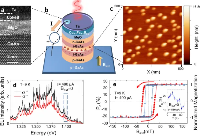
σ + σ - 1.325 1.350 1.400 EL In te nsi ty (a rb . u ni ts) 3 2 1 I= 490 µA Bext=0# 0 1.375 d T=9 K Energy (eV) Pc (% ) -20 -30 0 Bext(mT) 0 150 -150 T=9 K I= 490 µA e -50 50 -10 10 20 30 -100 100 T (K)# 0 40 80 10 20 15 Pc (% ) Bext=0# Height (n m) 16.86 0 X (nm) Y (n m) 0 500 0 500 Ta Co0.4Fe0.4B0.2 MgO n-GaAs i-GaAs i-GaAs p-GaAs+#
%#
p+-GaAs Bext" I 5000 4000 3000 2000 1000 0 5000 4000 3000 2000 1000 0 X[Å] Y [Å ] 16.86 nm 0.00 nm 5000 4000 3000 2000 1000 0 5000 4000 3000 2000 1000 0 X[Å] Y [Å ] 16.86 nm 0.00 nm I= 580 µA N orma lize d Ma gn et iza tio n 0 1 -1Figure 1: Spin LED device with p-doped InAs/GaAs quantum dots and polariza-tion resolved electroluminescence of an ensemble of quantum dots. a. High Resolupolariza-tion- Resolution-Transmission Electron Microscope image of the injector Ta/CoFeB/MgO/GaAs. b. Schematic structure of the spin-LED device. A single layer of InAs QDs is embedded in the intrinsic region of the p-i-n junction of the LED. c. AFM image of InAs QDs with a density of 1.6 × 10¹⁴ m−2. The average lateral dot diameter is about 30 nm and the height 9 nm. d. Electroluminescence from the device shows spectrally narrow emission lines stemming from an ensemble of semiconductor quantum dots. The applied magnetic field for the measurement is zero, and the magnetization of the CoFeB layer has been saturated before the measurements. σ+(σ−) polarized EL signal is plotted in black (red). e. The circular polarization degree of the EL (red circles) is plotted as a function of applied magnetic field Bextfor the ensemble emission of panel d. Hysteresis loop of the
normalized magnetization of CoFeB electrode measured by SQUID at T=30 K (blue squares). The inset shows the evolution of Pc with temperature at Bext= 0.
Pc (% ) 40 -10 20 0 -20 10 0 Bext(mT)% 0 150 -150 -40 Δz (µ eV) e f T=9 K I= 490 µA d Energy (eV) EL In te nsi ty (a rb . u ni ts) 2 1 0 Pc= 35 % Single quantum dot σ + σ - 1.3970 1.3975 1.3980 1.3985 Pc (% ) 15 20 25 30 I (mA)% 0 2 4 6 Bext=0% Bext=0 b σ - σ + Energy (eV) 1.3970 1.3975 1.3980 1.3985 EL In te nsi ty (a rb . u ni ts) 2 1 0 a EL In te nsi ty (a rb . u ni ts) 2 1 0 σ - σ + Pc= -35 % Bext=0 Bext=0 Energy (eV) 1.3970 1.3975 1.3980 1.3985 c g Bext= 0.8 T σ + σ - Energy (eV) 1.3970 1.3975 1.3980 1.3985 Δz=%57%µeV% Initial state before magnetic field saturation
Figure 2: Polarization-resolved electroluminescence of a single quantum dot and elec-trical nuclear spin initialization. a. Strongly polarized single dot emission at zero applied field (sweep direction negative to positive Bext). The background emission has been subtracted
for clarity. b. Unpolarized single dot emission before the first magnetization of the CoFeB layer c. Strongly polarized single dot emission at zero applied field (sweep direction positive to negative Bext). The polarization degree Pc is plotted as a function of the applied current in the inset. d.
Schematics of principle of the electrical initialization of nuclear spins in a single quantum dot at zero magnetic field due to efficient electrical spin injection in the dot combined with the hyperfine interaction between electron and nuclear spins. e. The circular polarization degree of the Elec-troluminescence is measured as a function of the applied magnetic field Bext. The sweep direction of the field is indicated by arrows. The data points corresponding to the initial magnetization are plotted in green. f. The energy difference ∆Z = Eσ+EL− EEL
σ− is plotted as a function of Bext. The
dashed line corresponds to the linear fit of ∆Z versus magnetic field for larger values of Bext. g.
Spectrally and polarization-resolved electroluminescence emission of a single dot at Bext= +0.8 T.
electron-nuclei hyperfine interaction. Nuclear spin polarization is reversed as we change the spin-orientation of the electrically injected electron spin. Controlling the nuclear spin bath in a dot in our Spin-LED is not just beneficial in order to potentially prolong carrier spin
life and coherence times [30, 31, 32], but the nuclear spins themselves with long relaxation
times are an interesting system for memory applications [33, 34, 35].
Polarization resolved electroluminescence of a quantum dot ensemble.— A
schematic of the Spin-LED structure is shown in Figure 1b. The spin injector consist of a
2.5 nm thick MgO layer and a 1.1 nm Co0.4Fe0.4B0.2 layer covered by a 5 nm Ta protection
layer deposited by sputtering. The p-i-n quantum dot (QD) LED device grown by MBE
contains a single layer of In0.3Ga0.7As QDs embedded in the optically active region with
Be delta doping (p-type) near the quantum dot layer (see methods). This favors the
for-mation of the positively charged exciton X+ (2 valence holes, 1 conduction electron). The
X+ consists of a hole spin singlet and an unpaired electron spin so the measured circular
polarization Pc in electroluminescence is directly given by the electron spin polarization as
Pc = −2hSezi where hSezi is the average electron spin projection onto the quantization axis
(here also growth direction) [28]. The measured EL degree of circular polarization is defined
as Pc = (Iσ+− Iσ−)/(Iσ++ Iσ−). Here Iσ+ (resp. Iσ− ) represents the integrated emission
intensity of the right (left) circularly polarized EL component. The thin CoFeB/MgO spin injector possesses a strong perpendicular-magnetic-anisotropy (PMA) due to the interfacial
anisotropy at the FM/Oxide interface [36]. Once its magnetization is saturated through
the application of a small out-of-plane magnetic field Bext, this material retains a remnant
out-of-plane magnetization even if the external field is switched off. This allows studying the spin-LED device with a magnetic electrode but at zero external applied field. The single dot electroluminescence (EL) is recorded at low temperature T=9 K in Faraday geometry, i.e. the magnetic field is applied along the growth axis, with a homebuilt confocal microscope
with a detection spot diameter of about 1 µm [37, 38], see methods.
Figure 1d displays the EL spectra measured at zero magnetic field, which shows an en-semble of many spectrally narrow emission peaks, centered at about 1.36 eV, corresponding to emission of a large number of QDs. The QD ensemble EL emission is strongly circularly
polarized with a large value of Pc = 23%, although the applied magnetic field is zero. Here a
DC voltage is used for LED operation, the generated current is sufficiently low (490 µA) to avoid any major impact of heating on the measurements. In Figure 1e we plot the degree of
circular polarization Pcof the ensemble EL of Figure 1d as a function of the applied magnetic
field Bext. We find for Pc clear hysteresis behavior as a function of magnetic field sweep
di-rection. This is in good agreement with the hysteresis loop of the normalized magnetization of CoFeB electrode measured by Superconducting Quantum Interference Device (SQUID)
5 Page 5 of 13
ACS Paragon Plus Environment
Nano Letters 1 2 3 4 5 6 7 8 9 10 11 12 13 14 15 16 17 18 19 20 21 22 23 24 25 26 27 28 29 30 31 32 33 34 35 36 37 38 39 40 41 42 43 44 45 46 47 48 49 50 51 52 53 54 55 56 57 58 59 60
at T=30 K on an unpatterned sample [26] (the slight discrepancy between the two curves is due to the difference in temperatures : 30 K instead of 9 K). This gives a strong indication that the EL polarization of the quantum dot emission is a reliable measure of the electron spin polarization, which in turn is determined by the out-of-plane magnetization of the FM
electrode. Our device shows an EL circular polarization degree Pc > 10% at zero field up to
liquid nitrogen temperatures, as demonstrated in the inset of Figure 1e. In previous studies application of magnetic fields of several Tesla was necessary to obtain strongly polarized EL
emission from a single quantum dot [22]. Here we achieve this goal in the absence of applied
magnetic fields.
Polarization resolved electroluminescence on a single quantum dot.— By using spectral filtering we are able to isolate the emission from a single quantum dot. In Figure
2a we show strongly circularly polarized emission with Pc = −35% at Bext = 0 when the
magnetic field is swept from negative to positive values. In contrast, when we sweep the
field from positive to negative values, we record at Bext = 0 a polarization of Pc = +35%
in Figure 2c. This strong EL polarization following injection of spin-polarized electrons is a
strong indication that the emission stems from the X+ trion [39]. In addition, the absence
of a clear doublet structure, as commonly observed for neutral exciton emission [25, 40] is
another typical feature of trion emission. For positively charged excitons, optical selection
rules yield Pc= −2hSezi. Therefore, the results in Figure 2a and 2c indicate that the initially
injected electron spin polarization is at least partially conserved during the radiative lifetime
of ≈ 800 ps [28,41](see discussion of nuclear spin fluctuations on electron spin decay below).
In the inset of Figure 2c, it is shown that the EL circular polarization decreases with increas-ing current. This could be due to an increase of the kinetic energy of injected electrons with applied bias so that electron spin relaxation via the Dyakonov-Perel mechanism becomes more efficient [42].
Hysteresis cycle of the electroluminescence polarization of a single QD.— The
measurements at Bext = 0 that result in strongly polarized EL rely on the PMA of the
CoFeB electrode. Now we want to study the EL emission of a single dot as a function of
the applied magnetic field Bext in more detail to check if the reversal of magnetization also
results in injection of electrons with the opposite spin and hence changes the sign of Pc. At
zero field, at the beginning of the measurements, the EL polarization is zero as shown in Figure 2b (see also the green points in Figure 2e). The domains in the electrode are initially
6
Page 6 of 13
ACS Paragon Plus Environment
Nano Letters 1 2 3 4 5 6 7 8 9 10 11 12 13 14 15 16 17 18 19 20 21 22 23 24 25 26 27 28 29 30 31 32 33 34 35 36 37 38 39 40 41 42 43 44 45 46 47 48 49 50 51 52 53 54 55 56 57 58 59 60
randomly magnetized (up and down), which results on average in zero magnetization for the CoFeB layer. When applying an external out-of-plane magnetic field, the domains are gradually magnetized along this field, resulting in an increase of the average spin of the
electrons hSezi injected into the quantum dot and therefore of the polarization of the emitted
light in EL. Once the magnetization is saturated, the CoFeB electrode presents a remnant magnetization when going back to zero magnetic field. Similar to the ensemble dot EL in Figure 1e, the circular polarization of the single dot EL changes sign at the critical fields around ±30 mT due to the switching of the CoFeB magnetization. The main difference between Figure 1e and Figure 2e is the overall polarization degree, reaching above 35% for the single dot compared to about 20% for the ensemble dot EL. The results in Figure 2e show the direct link between the observed EL polarization and the average electron spin for X+ emission as Pc= −2hSezi.
Zeeman splitting and nuclear spin polarization. More surprising are the results
shown in Figure 2f: here we plot the peak energy difference ∆z = Eσ+EL− Eσ−EL between the
σ+ and σ− polarized EL components as a function of the applied magnetic field. Whereas
at Bext> 100 mT the splitting ∆z is a linear function of Bext as expected (not shown), the
low and zero field data shown here exhibit again strong hysteresis, with the same coercivity
as that of the EL circular polarization. ∆z is measured to be up to 7 µeV at Bext = 0.
As-suming an electron g-factor for a typical InGaAs dot of |g| = 0.6 in ∆z(0 T) = geµBBn and
neglecting the hole-nuclear spin interaction [30] this corresponds to an effective magnetic
field of the order of Bn ≈ 200 mT experienced by the electron in the dot. The
ampli-tude of the splitting measured in EL is the signature of dynamic nuclear spin polarization
[43, 44, 45]. All nuclei in InGaAs carry a nuclear spin [43] and the hyperfine interaction
between carrier and nuclear spins has been shown to be very efficient in III-V quantum dots
[30, 44, 46, 47]. During the EL experiment, electrons with well oriented spin are injected
into the investigated dot. This electron spin polarization can be transferred in part to the
nuclear spin ensemble to create a non-zero average nuclear spin polarization hInzi. This is
seen by the electrons as an effective magnetic field Bn and results in a measurable Zeeman
splitting even at zero applied field (Overhauser shift), as clearly demonstrated before in
op-tical orientation experiments on single III-V dots [38, 48]. As the electron spin changes its
sign, also the effective nuclear field changes its direction and therefore the measured splitting
∆z changes its sign in the experiment in Figure 2f. The nuclear spin polarization is therefore
7 Page 7 of 13
ACS Paragon Plus Environment
Nano Letters 1 2 3 4 5 6 7 8 9 10 11 12 13 14 15 16 17 18 19 20 21 22 23 24 25 26 27 28 29 30 31 32 33 34 35 36 37 38 39 40 41 42 43 44 45 46 47 48 49 50 51 52 53 54 55 56 57 58 59 60
most likely at the origin of the hysteretic behavior that we find for the splitting ∆z around
zero magnetic field. An effective magnetic field Bn of about 200 mT will in part screen
the nuclear field fluctuations δBn, which are at the origin of electron spin relaxation and
decoherence [28,31,47,49]. The effective magnetic field Bndue to nuclear spin polarization
therefore helps to stabilize the electron spin polarization and thus to obtain highly circularly
polarized EL [50]. At higher applied fields the Zeeman splitting due to the external field
dominates the Overhauser shift.
In order to ascribe the observed splitting in EL at zero external magnetic field to nuclear spin effects, we need to exclude the impact of possible stray magnetic fields on the single dot EL, we show that these stray fields are negligible in the following: The stray field is well
known to be large (close to µ0MS, where Ms is the magnetization at saturation) inside the
ferromagnet due to the shape anisotropy and surface layer roughness does not change this value significantly. However, outside the ferromagnet but inside the semiconducting part of the device, the stray field is strictly zero in the absence of roughness, and negligibly small in a realistic situation. The roughness can be characterized by a modulation period of average
amplitude σ and lateral correlation length ξ [51]. Considering the first order frequency
contri-bution of the magnetic roughness (corresponding to a pure sinus shape roughness), the
max-imal value of the stray field can be written as Bmax = (µ0Ms/π)[1−exp(−2k00σ)]exp(−k00t),
where k00=
√
2π/ξ is the characteristic wavevector frequency along the two in-plane direc-tions and t is the distance from the bottom surface of magnetic layer to the quantum dot layer. From AFM measurements performed on the MgO/GaAs system, we have estimated the average surface roughness amplitude σ ≈ 0.3 nm and the correlation length ξ ≈ 50 nm.
Taking Ms = 6.35 × 10⁵A/m for a CoFeB layer thickness of 1.1 nm [26], and t = 95 nm leads
to an estimation of the stray field of around Bmax ≈ 2.6 µT. This is five orders of magnitude
smaller than the effective field Bn of roughly 200 mT extracted from our EL measurements
and can therefore not explain the observed splitting ∆z at Bext= 0 in Figure 2f. Note that
a characteristic noise function introduced in the roughness function would even lead to a smaller value of the stray field. Therefore, we can rule out the possibility that the stray field is at the origin of the effective magnetic field felt by the electrons in a quantum dot. In addition, we can see that the energy splitting is close to zero in the initial state when the injector is not magnetized (see green points in fig. 1e). This is another important argument for dynamic nuclear polarization being responsible for the observed splitting in EL emission
8
Page 8 of 13
ACS Paragon Plus Environment
Nano Letters 1 2 3 4 5 6 7 8 9 10 11 12 13 14 15 16 17 18 19 20 21 22 23 24 25 26 27 28 29 30 31 32 33 34 35 36 37 38 39 40 41 42 43 44 45 46 47 48 49 50 51 52 53 54 55 56 57 58 59 60
from an individual dot in the absence of any external magnetic field.
Conclusions.— We report strongly circularly polarized electroluminescence of a single InGaAs quantum dot in GaAs using an ultrathin CoFeB electrode. A polarization degree of up to 35% (20%) is observed for individual dots (dot ensembles) in the absence of applied external magnetic fields. This demonstrates that very efficient electrical spin injection and optical read-out of spin polarized electrons are possible in a single quantum dot without the need of an external magnetic field. Due to the efficient hyperfine interaction in III-V nanostructures, the repeated injection of spin polarized electrons into the dot leads to dy-namic nuclear polarization and hence a measurable Overhauser shift. This paves the way for highly circularly polarized compact light sources based on ensembles or single quantum dots, as well as electrical initialization of a single quantum bit carried by the electron spin, or alternatively by the nuclear spin ensemble in a single dot.
Methods.—
Sample growth: The p-i-n LED device grown by MBE contains a single layer of In0.3Ga0.7As
quantum dots embedded in the active region. The full sequence of the structure is the
following: p+-GaAs:Zn (001) substrate (p = 3 × 1018cm−3) | 300 nm p-GaAs:Be (p =
5×1018 cm−3) |400 nm p-Al0.3Ga0.7As:Be (p = 5×10¹⁷− 5 × 1018 cm−3) |30 nm GaAs with
Be delta doping near the QD layer and 1 layer of InGaAs cone-shaped quantum dots
(den-sity 1.6 × 10¹⁴ m−2, bottom diameter 30 nm, height 9 nm) |30 nm intrinsic GaAs |50 nm
n-GaAs:Si (n = 1016 cm−3). The LED was passivated with arsenic in the MBE chamber.
Then, the structure was transferred through air into a second MBE-sputtering intercon-nected system. The As capping layer is firstly desorbed at 300 deg C in the MBE chamber and then the sample was transferred through ultra-high vacuum to a sputtering chamber to
grow the MgO layer of thickness 2.5 nm. Finally, a 1.1 nm thick Co0.4Fe0.4B0.2 spin injector
and a 5 nm thick Ta protection layer are deposited by sputtering in both cases. Concerning the device fabrication, 300 µm diameter circular mesas were then processed using standard UV photolithography and etching techniques. Finally, the processed wafers were cut into small pieces to perform rapid temperature annealing (RTA) at 300 deg C for 3 minutes. More details of growth and optimization of the perpendicular spin-injector can be found in [8,26].
Transmission electron microscopy measurements: High-resolution transmission electron mi-croscopy (HR-TEM) studies were performed by using a JEOL ARM200 cold field-emission
9 Page 9 of 13
ACS Paragon Plus Environment
Nano Letters 1 2 3 4 5 6 7 8 9 10 11 12 13 14 15 16 17 18 19 20 21 22 23 24 25 26 27 28 29 30 31 32 33 34 35 36 37 38 39 40 41 42 43 44 45 46 47 48 49 50 51 52 53 54 55 56 57 58 59 60
gun working at 200 kV.
Optical characterization: The single dot electroluminescence (EL) is recorded in Faraday geometry with a home build confocal microscope with a detection spot diameter of 1µm
[37, 38]. The detected EL signal is dispersed by a spectrometer with 1200 grooves per
mm and detected by cooled a Si-CCD camera with the spectral precision of 2 µeV. The polarization analysis of the EL emission is performed with polarizers and achromatic
wave-plates. Magnetic fields Bext perpendicular to the LED are generated by a superconducting
coil inside a vibration-free closed cycle Helium cryostat, where the sample is mounted on nano-positioners.
AFM characterization: Samples are scanned by a Solver P47 system (NT-MDT) with reg-ular CONTACT mode.
Acknowledgments.— We acknowledge funding from ERC Grant No. 306719. F.C., P.R. and H.C. acknowledge the grant Next No ANR-10 LABX-0037 in the framework of the "Programme des Investissements d’Avenir". X.M. acknowledges Institut Universitaire de France. Y.L acknowledges the support by the joint French National Research Agency (ANR)-National Natural Science Foundation of China (NSFC) SISTER project (Grants No. ANR-11-IS10-0001 and No.NNSFC 61161130527) and ENSEMBLE project (Grants No. ANR-14-0028-01 and No. NNSFC 61411136001). A. D. acknowledges funding by Re-gion Lorraine.
[1] R. Fiederling, M. Keim, G. a. Reuscher, W. Ossau, G. Schmidt, A. Waag, and L. Molenkamp, Nature 402, 787 (1999).
[2] Y. Ohno, D. K. Young, B. Beschoten, F. Matsukura, H. Ohno, and D. D. Awschalom, Nature 402, 790 (1999).
[3] N. Nishizawa, K. Nishibayashi, and H. Munekata, PNAS 8, 1783 (2017).
[4] A. T. Hanbicki, O. M. J. van t Erve, R. Magno, G. Kioseoglou, C. H. Li, B. T. Jonker, G. Itskos, R. Mallory, M. Yasar, and A. Petrou, Applied Physics Letters 82, 4092 (2003).
[5] X. Jiang, R. M. Shelby, R. M. Macfarlane, S. R. Bank, J. S. Harris, and S. S. P. Parkin, Phys. Rev. Lett. 94, 056601 (2005).
[6] A. Fert and H. Jaffres, Phys. Rev. B 64, 184420 (2001).
10
Page 10 of 13
ACS Paragon Plus Environment
Nano Letters 1 2 3 4 5 6 7 8 9 10 11 12 13 14 15 16 17 18 19 20 21 22 23 24 25 26 27 28 29 30 31 32 33 34 35 36 37 38 39 40 41 42 43 44 45 46 47 48 49 50 51 52 53 54 55 56 57 58 59 60
[7] Y. Lu, V. G. Truong, P. Renucci, M. Tran, H. Jaffres, C. Deranlot, J. M. George, A. Lemaitre, Y. Zheng, D. Demaille, et al., Appl. Phys. Lett. 93, 152102 (2008).
[8] B. S. Tao, P. Barate, J. Frougier, P. Renucci, B. Xu, A. Djeffal, H. Jaffres, J. M. George, X. Marie, and S. Petit-Watelot, Appl.Phys.Lett. 108, 152404 (2016).
[9] C. Salter, R. Stevenson, I. Farrer, C. Nicoll, D. Ritchie, and A. Shields, Nature 465, 594 (2010).
[10] L. De Santis, C. Ant´on, B. Reznychenko, N. Somaschi, G. Coppola, J. Senellart, C. G´omez, A. Lemaˆıtre, I. Sagnes, A. G. White, et al., Nature Nanotechnology (2017).
[11] C. H. Li, G. Kioseoglou, O. M. van’tErve, M. E. Ware, D. Gammon, R. M. Stroud, B. T. Jonker, R. Mallory, M. Yasar, and A. Petrou, Appl. Phys. Lett. 86, 132503 (2005).
[12] G. Itskos, E. Harbord, S. K. Clowes, E. Clarke, L. F. Cohen, R. Murray, P. V. Dorpe, and W. V. Roy, Appl.Phys.Lett. 88, 022113 (2006).
[13] A. Merz, J. Siller, R. Schittny, C. Krammer, H. Kalt, and M. Hetterich, Appl.Phys.Lett. 104, 252401 (2014).
[14] G. Kioseoglou, M. Yasar, C. H. Li, M. Korkusinski, M. Diaz-Avila, A. T. Hanbicki, P. Hawrylak, A. Petrou, and B. T. Jonker, Phys. Rev. Lett. 101, 227203 (2008).
[15] M. Holub, J. Shin, D. Saha, and P. Bhattacharya, Phys.Rev.Lett. 98, 146603 (2007).
[16] R. Farshchi, M. Ramsteiner, J. Herfort, A. Tahraoui, and H. T. Grahn, Appl.Phys.Lett. 98, 162508 (2011).
[17] J. Xu, A. Lakhtakia, J. Liou, A. Chen, and I. J. Hodgkinson, Opt. Commun. 264, 235 (2006). [18] D. Y. Kim, J. Korean Phys. Soc. 49, S505 (2006).
[19] F. Henneberger and O. Benson, Semiconductor Quantum Bits (CRC Press, 2016).
[20] W. Loffler, M. Hetterich, C. Mauser, S. Li, and T. Passow, Appl.Phys.Lett. 90, 232105 (2007). [21] M. Ghali, T. Kummell, J. Wenisch, K. Brunner, and G. Bacher, Appl.Phys.Lett. 93, 073107
(2008).
[22] P. Asshoff, A. Merz, H. Kalt, and M. Hetterich, Applied Physics Letters 98, 112106 (2011). [23] P. Asshoff, G. Wust, A. Merz, D. Litvinov, D. Gerthsen, H. Kalt, and M. Hetterich, Phys.
Rev. B 84, 125302 (2011).
[24] M. Dyakonov, Springer Series in Solid-State Science, Springer-Verlag Berlin 157 (2008). [25] M. Bayer et al., Phys. Rev. B 65, 195315 (2002).
[26] S. H. Liang, T. T. Zhang, P. Barate, J. Frougier, M. Vidal, P. Renucci, B. Xu, H. Jaffr`es, J.-M.
11 Page 11 of 13
ACS Paragon Plus Environment
Nano Letters 1 2 3 4 5 6 7 8 9 10 11 12 13 14 15 16 17 18 19 20 21 22 23 24 25 26 27 28 29 30 31 32 33 34 35 36 37 38 39 40 41 42 43 44 45 46 47 48 49 50 51 52 53 54 55 56 57 58 59 60
George, X. Devaux, et al., Phys. Rev. B 90, 085310 (2014).
[27] S. Marcinkevicius, D. Siegert, and Q. X. Zhao, J. Appl. Phys. 100, 054310 (2006).
[28] P.-F. Braun, X. Marie, L. Lombez, B. Urbaszek, T. Amand, P. Renucci, V. Kalevich, K. Ka-vokin, O. Krebs, P. Voisin, et al., Physical review letters 94, 116601 (2005).
[29] X. Xu, Y. Wu, B. Sun, Q. Huang, J. Cheng, D. G. Steel, A. S. Bracker, D. Gammon, C. Emary, and L. J. Sham, Phys. Rev. Lett. 99, 097401 (2007).
[30] B. Urbaszek, X. Marie, T. Amand, O. Krebs, P. Voisin, P. Maletinsky, A. H¨ogele, and A. Imamoglu, Rev. Mod. Phys. 85, 79 (2013).
[31] A. Bechtold, D. Rauch, F. Li, T. Simmet, P.-L. Ardelt, A. Regler, K. M¨uller, N. A. Sinitsyn, and J. J. Finley, Nature Physics 11, 1005 (2015).
[32] G. ´Ethier-Majcher, D. Gangloff, R. Stockill, E. Clarke, M. Hugues, C. Le Gall, and M. Atat¨ure, Phys. Rev. Lett. 119, 130503 (2017).
[33] P. Maletinsky, M. Kroner, and A. Imamoglu, Nature Phys. 5, 407 (2009).
[34] A. M. Waeber, M. Hopkinson, I. Farrer, D. A. Ritchie, J. Nilsson, R. M. Stevenson, A. J. Bennett, A. J. Shields, G. Burkard, A. I. Tartakovskii, et al., Nature Physics 12, 688 (2016). [35] A. Greilich, A. Shabaev, D. Yakovlev, A. L. Efros, I. Yugova, D. Reuter, A. Wieck, and
M. Bayer, Science 317, 1896 (2007).
[36] S. Ikeda, K. Miura, H. Yamamoto, K. Mizunuma, H. Gan, M. Endo, S. Kanai, J. Hayakawa, F. Matsukura, and H. Ohno, Nature materials 9, 721 (2010).
[37] M. Vidal, M. V. Durnev, L. Bouet, T. Amand, M. M. Glazov, E. L. Ivchenko, P. Zhou, G. Wang, T. Mano, T. Kuroda, et al., Phys. Rev. B 94, 121302 (2016).
[38] G. Sallen, S. Kunz, T. Amand, L. Bouet, T. Kuroda, T. Mano, D. Paget, O. Krebs, X. Marie, K. Sakoda, et al., Nature Comms. 5, 3268 (2014).
[39] A. S. Bracker, E. A. Stinaff, D. Gammon, M. E. Ware, J. G. Tischler, A. Shabaev, A. L. Efros, D. Park, D. Gershoni, V. L. Korenev, et al., Phys. Rev. Lett. 94, 047402 (2005).
[40] D. Gammon et al., Phys. Rev. Lett. 76, 3005 (1996). [41] M. Paillard et al., Phys. Rev. Lett. 86, 1634 (2001).
[42] P. Barate, S. Liang, T. Zhang, J. Frougier, B. Xu, P. Schieffer, M. Vidal, H. Jaffr`es, B. L´epine, S. Tricot, et al., Physical Review Applied 8, 054027 (2017).
[43] E. A. Chekhovich, K. V. Kavokin, J. Puebla, A. B. Krysa, M. Hopkinson, A. D. Andreev, A. M. Sanchez, R. Beanland, M. S. Skolnick, and A. I. Tartakovskii, Nature Nanotech. 7, 646
12
Page 12 of 13
ACS Paragon Plus Environment
Nano Letters 1 2 3 4 5 6 7 8 9 10 11 12 13 14 15 16 17 18 19 20 21 22 23 24 25 26 27 28 29 30 31 32 33 34 35 36 37 38 39 40 41 42 43 44 45 46 47 48 49 50 51 52 53 54 55 56 57 58 59 60
(2012).
[44] D. Gammon, S. Brown, E. Snow, T. Kennedy, D. Katzer, and D. Park, Science 277, 85 (1997). [45] J. Strand, X. Lou, C. Adelmann, B. D. Schultz, A. F. Isakovic, C. J. Palmstrøm, and P. A.
Crowell, Phys. Rev. B 72, 155308 (2005).
[46] A. I. Tartakovskii, T. Wright, A. Russell, V. I. Fal’ko, A. B. Van’kov, J. Skiba-Szymanska, I. Drouzas, R. S. Kolodka, M. S. Skolnick, P. W. Fry, et al., Phys. Rev. Lett. 98, 026806 (2007). [47] H. Bluhm, S. Foletti, I. Neder, M. Rudner, D. Mahalu, V. Umansky, and A. Yacoby, Nature
Physics 7, 109 (2010).
[48] C. W. Lai, P. Maletinsky, A. Badolato, and A. Imamoglu, Phys. Rev. Lett. 96, 167403 (2006). [49] I. A. Merkulov, A. L. Efros, and M. Rosen, Phys. Rev. B 65, 205309 (2002).
[50] O. Krebs, B. Eble, A. Lemaˆıtre, P. Voisin, B. Urbaszek, T. Amand, and X. Marie, Comptes Rendus Physique 9, 874 (2008).
[51] P. Bruno, Journal of applied physics 64, 3153 (1988).
13 Page 13 of 13
ACS Paragon Plus Environment
Nano Letters 1 2 3 4 5 6 7 8 9 10 11 12 13 14 15 16 17 18 19 20 21 22 23 24 25 26 27 28 29 30 31 32 33 34 35 36 37 38 39 40 41 42 43 44 45 46 47 48 49 50 51 52 53 54 55 56 57 58 59 60