HAL Id: hal-02506174
https://hal.archives-ouvertes.fr/hal-02506174
Submitted on 12 Mar 2020
HAL is a multi-disciplinary open access
archive for the deposit and dissemination of
sci-entific research documents, whether they are
pub-lished or not. The documents may come from
teaching and research institutions in France or
abroad, or from public or private research centers.
L’archive ouverte pluridisciplinaire HAL, est
destinée au dépôt et à la diffusion de documents
scientifiques de niveau recherche, publiés ou non,
émanant des établissements d’enseignement et de
recherche français ou étrangers, des laboratoires
publics ou privés.
nano structures for power modules’ interconnection
Thomas Dias, Bojan Djuric, Vincent Bley, Olivier Dagut, Julien Morand,
Jean-Pascal Cambronne, Stefan Mollov
To cite this version:
Thomas Dias, Bojan Djuric, Vincent Bley, Olivier Dagut, Julien Morand, et al.. Optimization of the
manufacturing process of macro and nano structures for power modules’ interconnection. IMAPS,
POWER 2019, Nov 2019, Tours, France. �hal-02506174�
Optimization of the manufacturing process of macro and nano
structures for power modules’ interconnection
Thomas D
IAS12, Bojan D
JURIC23, Vincent B
LEY2, Olivier D
AGUT4, Julien M
ORAND3,
Jean-Pascal C
AMBRONNE2, Stefan M
OLLOV31Applied Physics & Electrical and Information Engineering Department, Ecole Normale Superieure Paris Saclay, Cachan, France 2Dielectric Materials in Energy Conversion, Laboratoire LAPLACE, Toulouse, France
3Mitsubishi Electric R&D Centre Europe, Rennes, France 4Universite Paul Sabatier, Toulouse, France
ABSTRACT:
This research aims at the development of a full direct copper interconnection for power modules. The focus lies on the optimization of the manufacturing process of this interconnection via electrodeposition. Particular attention is given to the current profile’s parameters to get high quality copper shapes.
Index Terms—Power electronics, Interconnection, Nano Wires, Packaging, Electrodeposition, PCB.
I. INTRODUCTION
L
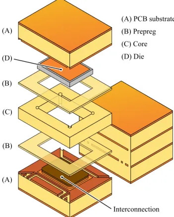
AST generation semiconductors have revolutionized power electronics in the past few years. The breakthrough of wide band-gap (WBG) materials has revealed the necessity to improve the power modules’ packaging. Power devices, based on silicon carbide (SiC) or gallium nitride (GaN), offer reduction of the switching time, a drastic increase in the switching frequency. This increase is generally correlated with a reduction in the passive components’ size. Nonetheless, the design of a low inductive switching cell is essential to take all benefits of the state-of-the-art semiconductors. The interconnections, between each switches and between switches and the decoupling capacitor in particular, are sources of stray elements and failures on power modules. The classical package interconnections use wire bonds on the top electrodes and the die attach is done by soldering on a substrate. This type of assembly, based on a 2D layout, creates high stray inductances, which combined with the fast switching transient, causes over-voltages. [8] Furthermore, the solder can lead to cracks due to a combination of a high temperature gradient and a mismatch in thermal coefficients in the assembly, which builds up during repeated cyclical stresses. [9] In most conventional cases, the component-substrate connection does not use all the useful surface of the electrode because it is restricted by the manufacturing constraints of wire bonding. On the other hand, the downsizing of the latest generation of WBG components is leading towards a reduced surface of electrode, revealing the limitations of the classical packaging technology. Fine feature connections are sought, which is new for power components. The Printed Circuit Board (PCB) embedding technology is foreseen as a good candidate for packaging WBG power devices. The current process is based on embedding the dies in a PCB substrate and to laser drill the interconnections(A) (B) (D) (A) (B) (C) Interconnection (A) PCB substrate (B) Prepreg (C) Core (D) Die
Fig. 1: Principle schematic of an interconnected die by nano-hairy macro posts in PCB environment
(microvias). This vertical layout, sometimes called 3D layout, allows to drastically decrease stray inductance of the switching cell. However, the microvias could suffer cracks due to the
endured cyclical stresses combined with the high ∆T during the module’s lifespan despite the double-sided cooling. [10]
The proposed solution [2] is also based on PCB-embedding technology, but interconnecting the die from both sides is done by a structure composed of a macro post overlaid by nano wires (figure 1). Solderless and (expected to be) flexible by the use of copper nano wires, this attach could improve the reliability of the module and to outperform the laser microvias interconnection.
The ohmic contact between the nano-hairy macro post and the active components is ensured by pressing of the nano wires’ tips against the copper metallization of the die. The height homogeneity is a key parameter to guarantee an even current distribution all over the electrodes and a good thermal path able to absorb the mechanical strains induced by the various CTEs.
II. CONCEPT OF THE INTERCONNECTION
The main concept of this interconnection relies on growing copper nano wires using electrodeposition with a patterned mask. A porous alumina membrane containing 60 µm deep wells is used as a mask. A step-by-step description of the process is done here after.
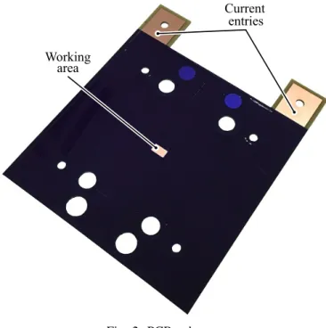
At first, a photosensitive film is deposited on the PCB substrate (fig. 2) to define the interconnection area from the rest of the copper. Then, an opening is made to expose the working area which will form the interconnection. The membrane has to be pressed on a flush surface to avoid any damages. Therefore, a macro post (full copper metallization) is deposited to fill the opening in the dry film and to obtain a flat surface between the film and the macro post. Prior each electroplating, an electro-etching step is made to increase the adhesion of the following copper deposition).
Current entries Working
area
Fig. 2: PCB substrate
Subsequently, the membrane is pressed against the photo-sensitive film and the macro post. Multiple layers of cellulosic
paper soaked with copper sulfate is used as a buffer solution to homogenize the mechanical strains on the membrane. A copper counter electrode is pressed on top of this set-up and the assembly is tightened with a controlled torque to achieve repeatability. With this configuration, a partial filling of the pores is done during around 14% of the total deposition time. This results in a filling ratio of 70% of the surface covered with a few µm tall nano wires. The presence of the nano wires has the effect of retaining the membrane in position. With the counter electrode at a small distance from the working area, the deposition is highly promoted in the centre of the working area. The pressing step, although essential to maintain the membrane, is reducing the homogeneous deposition of the nano wires, especially in terms of height.
At this stage, the remaining membrane filling is done with the counter electrode distanced from the PCB substrate like in conventional PCB electrodeposition. This allows a better circulation of the electrolytic solution near the working area and promotes the homogeneity of the deposition. At the end of this step, the complete filling of the membrane is achieved, with the copper nano wires’ tips being close to the top of the membrane. Finally, the membrane and dry film are dissolved using sodium hydroxide. The obtained interconnection is a macro post completely covered by nano wires with a total height around 100 µm (fig. 3).
20 µm 103.2 µm 48.5 µm 44.7 µm Nano wires Macro post Base plate
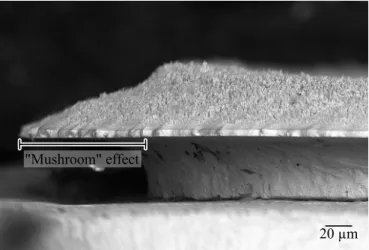
Fig. 3: Vertical SEM acquisition of the interconnection It can be seen on figure (3) that a ”baseplate” is formed between the nano wires and the macro-post. This is due to the beginning of copper deposition between the membrane and the macro-post - the surface formed by the macro post and the photosensitive film is not perfectly flat, which creates a gap. This baseplate is seen to extend further than the macro post itself. This phenomenon shapes the assembly like a mushroom as it can be seen on figure (4). One can also observe that the nano wires also grow on the extremities of the baseplate but the pores are fully filled (i.e. the nano wires are fully grown) only when the macro post is present under them.
III. CURRENT PROFILES EXPLORATION
Electroplating is a well-known process in the PCB industry, for plating through holes (PTH) and filling vias. Usually done
20 µm "Mushroom" effect
Fig. 4: Baseplate creating the ”mushroom” effect
with a direct current (DC), this process relies heavily on the presence of additives (accelerator, suppressor and leveler) to shape the deposition according to needs. However, this is not an easy task when it comes down to the micro or nano-meter precision with a DC profile. Recent work by Feng et al. [3] made on microvias has shown the limits of a DC deposition for this technology. A pulsed current profile was therefore applied in order to fill the microvias without any resulting cavity.
Different pulsed current profiles can be used, to obtain the desired result. Research [1, 4, 6] have shown the advantages of Pulsed Current (PC) profiles with relaxation after the pulse, while others prefer to use forward and reverse pulses, with or without relaxation between the pulses. A reverse pulse has the effect of mainly etching the peaks of the working area, acting as a leveling phase. By modulating the reverse pulse’s duration, it is possible to either smooth the roughness or to etch evenly the whole surface. Introducing reverse pulses can be used to homogenize the deposition. [5] The complexity of the different pulsed profiles lies on finding the right set of parameters (current density and duration of the pulses, frequency of the signal, duration of the relaxations) in order to obtain a uniform electroplating.
The deposition rate is given by Faraday’s law (1), with the deposition rate hτ (µm/s), the mean current I (A), the molar volume Vm(mol/µm3), electrode area S (µm2), the number
of electrons involved n and the Faraday’s constant F (C/mol). It can be seen that the deposited height depends on the average current of the profile and the time of deposition. Previous studies have also shown the importance of the waveform of the current itself. While continuous waveforms tend to accentuate inhomogeneities of the deposit, pulsed profiles can be tailored to the application’s needs.
h τ =
VmI
nF S (1)
Figure (5) shows the different current profiles selected in our experiments and table I lists the main features of each profile. The pulses’ current density is limited to a maximum of 30 mA/cm2 for all profiles, which are all maintained in the few Hz frequency range. This allows us to obtain the fastest deposition rate while varying the time parameters
Reverse Relaxation Pulse X X X X X X X X P PR PPR PPRR Wave
TABLE I: Features of the current profiles
(periods of pulses). All the following experiments were done until the filling of the membrane was achieved. They will be compared in terms of height homogeneity through the waviness parameter and height difference between the nano-wires.
Fig. 5: Current profiles used
A. Direct current profile
Following the recommendations of the electrodeposition bath manufacturer, a first experiment was made with a constant current density of 30 mA/cm2. This will be used as a refer-ence in our comparison. Its advantages are the fast deposition and ease to apply. In our case, the total manufacturing is only 1h30 with this current profile.
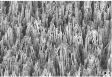
Although the deposition is fast, the SEM acquisition in figure (6), shows a great inhomogeneity in the growth. The nano wires have overflowed from the pores in the middle and borders of the working area. The rest of the pores are less filled or not at all. In addition, the nano wires are not exactly wires, but rather tubes. A hollow section inside the wires can be observed, with a diameter of around 100 nm. The tubes have around 25% less copper than ”normal” wires.
This shows that the fast deposition using direct current is not an acceptable solution to manufacture the nano wires for a power module interconnection. The deposit is extremely inhomogeneous and the lack of copper in the inner section of the pores does not correspond to the objective of reducing electrical and thermal resistance.
3 µm Fig. 6: SEM acquisition of a DC deposition
B. Pulsed (P) profile
The second tested profile is the pulsed profile (red curve on figure 5). This profile is composed of a 50 ms pulse with a current density of 30 mA.cm−2 and a 250 ms pulse with a current density of 2 mA.cm−2.
In this configuration, the total deposition took in 6h53. Although it is very time consuming, this set-up results in a very homogeneous interconnection.
2 µm Fig. 7: Pulse superposition SEM acquisition (top view) One can see on figure (7) that the waviness of the deposition is better than DC profile on figure (6) and seems very low. The nano wires’ height difference is also very small when compared to other current profiles. The nano wires show a high quality, with few physical defects. Some samples showed small protrusions around the tips of the wires, but the vast majority were similar to figure (7).
C. Pulsed relaxed (PR) profile
As stated in previous sections, the relaxation introduced after a pulse serves the purpose of renewing the solution near the working area. A 50% duty cycle is used, forward pulse with a 30 mA.cm−2. This pulse is followed by a total relaxation at zero current.
3 µm Fig. 8: Pulse profile SEM acquisition
This profile’s sample (figure 8) appears to have a much higher difference between nano wires’ height than our refer-ence deposition. A differrefer-ence of around 6 µm can be observed, which is 10% of the expected nano wires’ height. There is also a high amount of visible defects. The wires present a unneglectable porosity, which results in weaker wires and higher electrical and thermal resistance. Moreover, the border effects were more visible than with previous experiments. The border effect causes the nano wires on the border of the macro-post to be higher than the rest. This is the worst case possible since a high border effect could cause the breaking of the active component pressed against the interconnection. Therefore, this current profile is also not acceptable for our application, even if the deposition time is the lowest of the pulsed profiles, needing 3 hours to fill the membrane. A high roughness is not sought since the objective is to maximize the contact between an active component and the interconnection.
D. Periodic Pulse Reverse (PPR)
The Periodic Pulse Reverse current profile was used in order to obtain a more homogeneous interconnection’s height. The fast reverse pulse tends to etch the copper that is closer to the counter electrode. Meaning that the highest nano wires (i.e. which growth was favored) are slightly shortened during each reverse pulse. For this profile, a ratio of one half to one third is selected between the forward and reverse pulse’s amplitude. [7] Their periods have a ratio of around 20, with a total period of 300 ms.
This deposition shows (figure 9) a very homogeneous nano-wires’ height over the whole interconnection, but a difference between nano wires’ height around 5 µm. The obtained result is similar to the pulsed profile on figure (7). Despite a low electroplating duration (3h30), the nano wires are forming aggregates. Many defects called dry earth are noticeable, which decreases the contact surface and thus increasing the electrical and thermal resistance.
E. Periodic Pulse Reverse Relaxed
Based on the previous results, a final current profile is pro-posed, in order to take all the benefits from both the relaxation
8 µm Fig. 9: Periodic Pulse Reverse sample SEM acquisition
and reverse pulse seen before. The objectives are to make the deposition more homogeneous and to relax the solution for the coming deposition. The profile is a combination of the PPR profile and a 50 ms relaxation step added after the reverse pulse.
3 µm Fig. 10: Periodic Pulse Reverse Relaxed sample SEM
acquisition
This resulting deposition shows (figure 10) a similar wires’ height difference as in the pulsed profile. The nano wires do not present visible defects. It seems, however, to produce a higher ”mushroom” effect. The baseplate grows further on the side of the macro-post than with the pulsed profile. This deposition shows similar characteristics to the pulsed profile, with a smaller manufacturing time. Therefore, it is a serious candidate for the interconnection manufacturing.
IV. MATERIALS AND METHODS
A Bungard COMPACTA 30 electroplating machine with a copper sulfate acidic bath is used, with Bungard Cu400A pro-prietary solution as brightener. The PCB substrates are made of 0.8 mm Arlon 35N dielectric with 105 µm thick copper layers. The counter electrode (anode) is a 99.9% pure copper 2” diameter disk. The physical set-up for our experiments consists in a PMMA support with the PCB maintained against
it. The counter electrode is placed on top of the working area distanced by 1 cm nylon spacers. The profile is applied by a Keithley 2612A Source Measure Unit (SMU).
The bath temperature was at room temperature and no influence on the deposition dynamics was observed between 25 and 30◦C. However, experiments were made by using both galvanically insulated channels of the SMU to deposit on two PCB substrates at the same time. The results showed a slightly faster deposition, which allowed the reduction of the macro-post’s manufacturing time from 6h53 to 6h38, with the superposition of pulses.
V. CONCLUSION AND OUTLOOK
This paper is aimed at the optimization of the manufactur-ing process of an innovative power device interconnection. The challenges are to minimize the electrical and thermal resistance. To achieve the desired performances, experiments were conducted to understand the effect of the different current profile’s parameters.
Table (II) gives an overview of the characteristics of each current profile. It can be seen that two profiles achieved similar results. The superposed pulses are an efficient technique to obtain very homogeneous nano wires’ height. However, the manufacturing time is close to 7 hours. In order to reduce this time, the PPRR profile can be used and achieve very similar homogeneity but the mushroom effect is then more pronounced.
The need of the macro-post is a troublesome step since it doubles the total manufacturing time. A solution where the membrane would be pressed directly against the PCB substrate would remove the need for the macro-post. Further investigation on the influence of the current’s parameters together with additive agents could be conducted to improve the manufacturing process.
PPRR PPR PR P DC 60 µm 1 µm 6 µm 10 µm 2 µm Nano wires' height diff. "Mushroom" effect Wire defects Time 200 µm 20 µm 20 µm 40 µm 100 µm Tubular None Holes None None 1h30 6h53 3h00 3h30 4h00 TABLE II: Recap of the characteristics of the depositions
VI. ACKNOWLEDGEMENT
The authors thank the SCEL from University of Paul Sabatier, Toulouse 3 for giving their assistance and the access to the lab scale PCB production line equipment.
REFERENCES
[1] M. S. Chandrasekar and Malathy Pushpavanam. Pulse and pulse reverse plating-Conceptual, advantages and applications, 2008.
[2] Bojan Djuric, Vincent Bley, Julien Morand, Olivier Dagut, Jean-Pascal Cambronne, and Stefan Mollov. Dou-ble side interconnection for vertical power components based on macro and nano structured copper interfaces and printed circuit board technologies. In MINAPAD. France, 2019.
[3] Kesheng Feng, Bill Decesare, Mike Yu, Don Desalvo, and Jim Watkowski. Electroplated copper filling of through holes on varying substrate thickness. 2014 9th International Microsystems, Packaging, Assembly and Circuits Technology Conference: Challenges of Change -Shaping the Future, IMPACT 2014 - Proceedings, pages 355–358, 2015.
[4] Kousik Ganesan, Yang Sun, Chandrasekhar Pendyala, Radek Chalupa, Suddhastawa Nad, Thomas Heaton, Mar-cel Wall, Rahul Manepalli, and Amaneh Tasooji. Innova-tive Advances in Copper Electroplating for IC Substrate Manufacturing. In Proceedings - Electronic Components and Technology Conference, 2017.
[5] Show-Chin Kou and Aina Hung. Studies of Acid Sulfate Copper Pulse Reversal Current Electrodeposition. Plating & Surface Finishing, (135):140–144, 2000. [6] Peter Kristof and Mark Pritzker. Improved Copper
Plating Through the Use of Current Pulsing & Ultrasonic Agitation. Technical report, 1998.
[7] Bernadette NGUYEN. Electrod´eposition par courants´ puls´es. Techniques de l’ing´enieur, 1998.
[8] Jukkrit Noppakunkajorn, Di Han, and Bulent Sarlioglu. Analysis of High-Speed PCB with SiC Devices by vestigating Turn-Off Overvoltage and Interconnection In-ductance Influence. IEEE Transactions on Transportation Electrification, 1(2):118–125, aug 2015.
[9] Uwe Scheuermann and Ralf Schmidt. Impact of Solder Fatigue on Module Lifetime in Power Cycling Tests. In Proceedings of the 2011 14th European Conference on Power Electronics and Applications, pages 1–10, 2011. [10] Bingshou Xiong, Kum Weng Loo, and Kumar Nagarajan.
Microvia reliability improvement for high density inter-connect substrate. In Electronics Packaging Technology Conference, pages 138–141. IEEE, 2011.