HAL Id: hal-03184429
https://hal.archives-ouvertes.fr/hal-03184429
Submitted on 29 Mar 2021
HAL is a multi-disciplinary open access
archive for the deposit and dissemination of
sci-entific research documents, whether they are
pub-lished or not. The documents may come from
teaching and research institutions in France or
abroad, or from public or private research centers.
L’archive ouverte pluridisciplinaire HAL, est
destinée au dépôt et à la diffusion de documents
scientifiques de niveau recherche, publiés ou non,
émanant des établissements d’enseignement et de
recherche français ou étrangers, des laboratoires
publics ou privés.
Space charge measurements on electron-beam irradiated
LDPE films, with and without metallization of
irradiated surface
Mallys Banda, Virginie Griseri, Séverine Le Roy, G. Teyssedre
To cite this version:
Mallys Banda, Virginie Griseri, Séverine Le Roy, G. Teyssedre. Space charge measurements on
electron-beam irradiated LDPE films, with and without metallization of irradiated surface. French
Electrostatics Society, Aug 2016, Poitiers, France. �hal-03184429�
I. INTRODUCTION
Because of their good electrical, mechanical or thermal properties, solid organic materials are increasingly used as insulators in embedded systems, energy transport or space environment. However, these insulating materials can accumulate electrical charges when exposed to various stresses, such as radiation, electric field, temperature or humidity. When the quantity of accumulated charges increases, electrical field distortion as well as energy release may lead to damages to the material and to irreversible loss of the initial insulating performances. The investigation of space charge distribution in irradiated polymers is an original way to understand charges transport and accumulation mechanisms within charged solid dielectrics [1-3], as charge generation is mainly due to charge deposition by the electron beam.
In this study, LDPE films of different thicknesses, metallized and non-metallized, were irradiated by electron-beam in open-circuit conditions. Space charge distributions recorded in open circuit configuration and their corresponding electric field distributions are presented and discussed.
II. METHODOLOGY
A. Samples processing
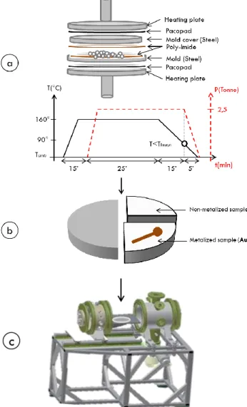
Samples of different thicknesses, ranging from 200 µm to 300 µm, and 80 mm in diameter, were prepared from LDPE pellets, using a hydraulic press. The pellets were heated between two plates, from ambient temperature to 140°C, at atmospheric pressure. A pressure of 2.5 bars was then applied on the sample during 25 minutes, as sketched in Fig. 1a and finally cooled to room temperature with maintaining the pressure.
Fig. 1. Experimental steps of film preparation and measurement. a) LDPE films preparation technique (set-up and protocol), b) Gold metallization, c) Installation into irradiation chamber - Matspace.
Space charge measurements on electron-beam irradiated LDPE films, with
and without metallization of irradiated surface
M. E. Banda, V. Griseri, S. Le Roy, G. Teyssèdre
LAPLACE, Université de Toulouse, CNRS, INPT, UPS, France
Abstract—One way to characterize and to model charge transport mechanisms in dielectric materials consists of
irradiating them with an electron-beam and observing their electrical response. For that purpose, Low Density Polyethylene (LDPE) films of different thicknesses were irradiated by a 80 keV electron beam in an open-circuit configuration. Space charge measurements were performed using the Pulse Electro-Acoustic (PEA) method ‘without contact’. Profiles were acquired every two minutes of irradiation for 8 minutes, followed by 24 hours of relaxation under vacuum. The impact of metallization on the irradiated surface as regards the charges transport and generation phenomena are presented and discussed. Even though the deposited electrode was under floating potential, it is shown that the charge and field distribution during irradiation of the dielectric is not the same as without metallization. One clear feature is the build-up of a positive charge onto the electrode during irradiation, which is presumably due to secondary electron emission from the electrode. As a consequence, the equivalence in sample conditioned with or without floating electrode cannot be claimed.
Keywords— Space charge, electron-beam irradiation, Pulsed Electro-Acoustic method (PEA), polyethylene.
The deposition of a metallic electrode on the sample was achieved in the perspective of driving charges into the material while imposing the field, or to make post-irradiation measurements as conduction current or electroluminescence. Our purpose here is to evaluate the impact of this metallization onto the fate of deposited charges into the insulation. To do so, a thin layer of gold, 50 nm in thickness and 80 mm in diameter, was deposited on a part of each film, as shown in Fig. 1b, by cold sputtering. The deposition rate was 0.1 nm/s and the sample was cooled during the process.
Finally, LDPE metallized samples were inserted in the Matspace irradiation chamber, with features as described elsewhere [4] where they were maintained under secondary vacuum (
6
.
5
10
6mbar
) for 24 h before anyirradiation was performed.
B. Irradiation conditions :
LDPE films were irradiated under vacuum conditions with a 80 keV electron beam source under a flux Io of
1 nA/cm2, by step of 2 minutes for 8 minutes only, to prevent any discharge due to a too high surface potential. Each 2 minutes, the irradiation was stopped to perform a space charge measurement using the PEA set-up in non-contact mode [5]. The time spent between two irradiation steps is about 1 min. For exciting the material, voltage pulses of 1.5 kV amplitude and 9 ns width were applied to an upper electrode placed in front of the irradiated area. The gap between the irradiated surface of the dielectric and the upper electrode that is grounded is of the order of 1 mm.
Fig. 2. Model of open-circuit set-up for electron-beam irradiation on non-metallized LDPE film.
The classical model presented in the literature [1-2] describing the charges build-up and transport during and after electron-beam irradiation of a sample of thickness d is depicted in Fig. 2. Once the irradiation starts, electrons are deposited within the dielectric following the decay in primary electron flux I(z). The dielectric is divided into two zones, an irradiated zone where negative charges are deposited, and a non-irradiated zone. In the literature [1-2], the irradiated zone has electrical properties (mainly conductivity) that become different from those of the non- irradiated one, owing to electron-hole generation pairs –
g(z,t) along with possible material alteration due to the
ionizing radiation.
The electric field profile is calculated from the distribution of the net charge density, (z,t) using
Poisson's equation:
( , ) ) , ( z t z t z E (1)With the adopted representation, a negative charge implanted in the dielectric produces a positive field in the non-irradiated region.
III. EXPERIMENTAL RESULTS
A. Results without metallization on the irradiated surface
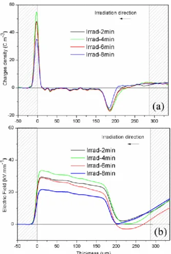
Measurements were first performed on a non-metallized LDPE film of 286 µm thickness. The charge distribution was recorded each 2 minutes of irradiation for 8 minutes. The charge distributions and corresponding electric field distributions are shown in Fig. 3. The maximum electron deposition is located at 100 µm from the irradiated face, which is consistent with theoretical calculation estimated from [6] at 99.2 µm.
Fig. 3. (a) Space charge profiles in LDPE film of 286 µm thickness irradiated for 8 min by a 80 keV electron-beam at 1 nA/cm2, (b) Electric field associated with the space charge profile.
During the first minutes of irradiation, implanted charge density progressively increases in the dielectric bulk with the irradiation time. After 6 minutes of irradiation, the maximum implanted charge density remains below -20 C/m3. The maximum charge density decreases then at 8 minutes of irradiation.
The decrease of the charge density for the last irradiation step is also observable on the image charge at the grounded electrode (left). This could be due to the way of measuring the space charge, as the irradiation is stopped for a while in order to make the PEA measurement, or to charge reorganization inside the dielectric, leading to a small decrease of the net charge. The electron-beam not only deposits negative charges inside the dielectric, but also creates electron-hole pairs. A movement of these charges, due to the electric field (Fig. 3b), i.e. negative charges drifted towards the left electrode and positive charges tending to stay at around 100 µm from the irradiated face, could also explain this small decrease of the net charge after 8 minutes of irradiation. This non-metallized film was kept during relaxation inside the irradiation chamber under secondary vacuum conditions and charges distributions were measured each hour. Fig. 4 presents the space charge profiles and associated field profiles during the relaxation phase.
Fig. 4. (a) Space charge profiles and (b) associated electric field profiles in a 286 µm thick LDPE film during relaxation after electron beam irradiation under 80 keV at 1 nA/cm2.
Starting from the last distribution under irradiation, the peak of implanted charges continuously decreases, the peak amplitude being at 55% of the initial amplitude after 24 hours of relaxation. The implanted charges are drifted toward the grounded electrode, under the effect of the positive electric field (Fig. 4b). Hence, the electric field in the irradiated zone decreases with the relaxation time. Although the decrease of charge reaches more than 50%, the net charge remaining after 24 hours of relaxation is still high, i.e. the charges are difficult to extract from the dielectric under vacuum conditions.
B. Results with metallization on irradiated surface
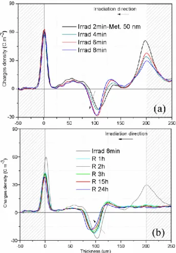
Fig. 5. Space charge profiles in LDPE film of 200 µm thickness metallized (50 nm Au) on its irradiated face, (a) during irradiation with a 80 keV electron-beam at 1 nA/cm2, and (b) during relaxation.
Measurements were performed under similar conditions with a 200 µm thick metallized LDPE film. This one was metallized with a gold layer of 50 nm thickness. The metallization was deposited on the irradiated face only. Following the same irradiation and relaxation protocol, the charges distribution was measured with the open-circuit PEA. As presented in Fig. 5a), the peak of negative charges is still located at 100 µm from the irradiated face, as for the non-metallized sample. The peak maximum also shifts towards the ground electrode with irradiation time. The charge density within the dielectric grows with the irradiation time. At the end of irradiation, the peak
maximum is of the order of 30 C/m3, one and a half more than what has been observed without metallization (Fig. 3). Positives charges are also detected in the bulk of the insulation some minutes after irradiation.
These positive charges were not observed without metallization. Moreover, a large amount of positive charges appears at the irradiated face, which is metallized. The origin of positive charges in the bulk is probably due to the creation of electron/hole pairs due to electron beam irradiation. These positive charges, once created, are also submitted to the electric field, and tend to accumulate at the vicinity of the negative charge peak, i.e. where the electric field changes of sign (fig. 4b). Moreover, as negative charges drift towards the ground electrode, they also 'uncover' the positive charges in this region. The origin of the positive charge on the irradiated face is however less clear, and further measurements were performed in order to understand this particular feature.
During relaxation (fig. 5b), the negative charge peak still moves towards the ground electrode, and the amplitude of the charge peak decreases with relaxation time. Fig. 6 shows another example of charge relaxation of a metallized LDPE film of 250 µm thickness, after irradiation for 8 min with the protocol previously described. For this relaxation it is clear that negative charges move towards the ground electrode, and are either accumulated at the electrode, or extracted there. It also means that the electric field, with amplitude of the order of 30-40kV/mm, is favorable to positive charges injection at this electrode. Hence, it is possible that negative charge accumulation is hidden by positive charge build-up resulting from charge injection.
Fig. 6. Space charge profiles during relaxation of a metallized LDPE film of 250 µm in thickness.
The positive charge peak in the non -irradiated zone (left side of the negative peak) tends to decrease, due to the drift of negative charges, that decreases the net charge density. The positive charge peak in the irradiated zone (right side) increases, as during irradiation, due to the movement of negative charges towards the ground electrode. The large amount of positive charges that
appeared on the irradiated face disappears within the first minutes of relaxation.
IV. DISCUSSION
The experimental results show an electron implantation in the bulk of dielectric during irradiation. The maximum peak of these negative charge deposited by the electron-beam is localized at 100 µm from irradiated face, as theoretically predicted. In the case of non-metallized samples, the implanted negative charge peak increases during the first minutes of irradiation and stabilizes at about 6 minutes, before decreasing. This stagnation of negative charge amplitude could be explained by a progressive extraction of implanted electrons and the injection of reciprocal positives charges at the left electrode [7].
When a metallization -with floating potential- is previously deposited on the irradiated face, positive charges appear in the bulk and on the metallized surface. Positive charges are often observed in electron-beam irradiation on polymeric materials [3,7], and have already been interpreted in terms of charge generation, either by creation of electron/hole pairs due to the beam, or by charge injection at the ground electrode. Few studies refer to positive charges on a metallized-irradiated face. Note that in the actual measurement configuration of the PEA method, acoustic waves propagating into the material are totally reflected at the dielectric/vacuum interface. As a consequence, charge clouds located at the surface or within a distance from the surface less than the resolution of the method appear with a density over-estimated by a factor 2 [8].
In a first guess, one could think that the presence of these positive charges on the metallized face is due to a bad contact on the irradiated face, leading to grounding on this face and to the build-up of an image charge (as for the ground electrode). But care has been taken to reproduce the measurement, and these positive charges on the irradiated face are still present, and cannot be due to an error in the set-up. In addition, these positive charges, present during irradiation, disappear as soon as the electron-beam is stopped, a feature that is not expected for an influence charge. Electrons arising from the beam could also interact with the thin gold layer.
Measurements have been performed on LDPE sample with different metallization thicknesses, ranging from 50 to 150 nm, in order to check if the gold thickness plays a role in the positive charge appearance. The same protocol is applied for each sample, and Fig. 7 presents the space charge profiles for the different metallization thicknesses after 8 minutes of irradiation. It can be observed that the thicker the metallization is, the lower and the broader the negative charge peak in the dielectric. This can also be seen with the image charge at the ground electrode, on the left side. Moreover, it seems that the location of the negative peak maximum is around 100 µm for 50 and
100 nm of metallization, but is around 80 µm for 150 nm of metallization.
Fig. 7. Space charge profiles in post-irradiation of metallized LDPE film of 250 µm thickness.
Primary electrons, arising directly from the beam, interact with the matter:
- they transfer part or the totality of their energy to the matter (electrons, nucleus..), leading to electrons that have a lower energy compared to the one of the electron beam ; - they create, due to a transfer of energy, secondary electrons arising from atoms of the metal, with energy much lower than that of the primary electron beam.
Some of the secondary electrons created are extracted letting the gold layer globally positively charged during irradiation. This could be the origin of the positive charge peak at the irradiated face.
The energy loss of the primary electrons could explain the decrease of the electrons density being measured in the dielectric, and the broadening of the peak as well as the decrease of the penetration depth for a metallization of 150 nm, due to the decrease of the energy of the electrons. The behavior of the positive charge on the irradiated face could also be explained by the extraction of electrons from the metal, leading to a global positive charge on the metal layer. This positive charge only holds as long as the irradiation is on. Once the irradiation stops, the rearrangement of the electrons in the metal quickly leads to a zero charge on the irradiated face. However, the behavior of these positive charges is a bit more hazardous, and there is no linearity as a function of the metallization thickness.
Positive charges in the bulk on each side of the negative charges peak are observable for 50 and 100 nm metallization, and not for 150 nm.
One main remaining question is if the presence of these charges on the irradiated face disturbs the electric field distribution in the dielectric during irradiation, and hence refrains from comparing non metallized samples to metallized ones. It could be the case during irradiation, as positive charges are observable for metallized samples only. During relaxation, the space charge profiles seem to
become comparable after a long relaxation time, as positive charges seem to disappear with time. However, with a longer irradiation time, the space charge profiles could differ to a larger extent.
V. CONCLUSION
In this study, the space charge measurements on electron-beam irradiated LDPE films with and without metallization on its irradiated surface were presented and discussed. The impact of metallization as regards the generation and transport phenomena is highlighted. Some conclusions can be drawn:
Negative charges implanted by electron-beam are observed at 100 µm from irradiated surface, with and without metallization ;
In the case of metallized samples only, a non-negligible amount of positive charges appears in the bulk on each side of the negative charge peak, and on the irradiated film surface, whatever the metallization thickness ;
During relaxation, the implanted charges mainly migrate toward grounded electrode, thus illustrating the transport within the dielectric.
Metallization on the irradiated face could have a non-negligible impact on the space charge profiles during irradiation with an electron beam. The electric field distribution, being different for metallized sample compared to non-metallized one, drives a redistribution of the charges due to charge transport, even during irradiation, where electron beam phenomena (i.e. charge deposition and creation of electron/hole pairs) should be dominant. As metallization can be a prerequisite to further measurements like e.g. post-irradiation conductivity or electroluminescence, one cannot at the moment claim on the rigorous equivalence of e-beam conditioning of films with and without electrodes, would it be a thin electrode.
REFERENCES
[1] B. Gross and L. N. de Oliveira. “Transport of excess charge
in electron-irradiated dielectrics”, J. App. Phys., Vol. 45, pp. 4724-4729, 1974.
[2] G. M. Sessler, “Charge dynamics in irradiated polymers”,
IEEE Trans. Dielectr. Electr. Insul., Vol. 27, pp. 961-973, 1992.
[3] N. Tomite, Y. Arai, Y. Ohki, H. Nakamura, T. Hinata, M.
Washio, "Space charges induced in polymers by electron beam irradiation and their decay profiles." Proc. IEEE Int. Conference on Solid Dielectrics (Bologna, Italy), pp. 736-739, 2013.
[4] V.Griseri, et al. “Charge build-up and transport in electron
beam irradiated polymers in a new irradiation chamber,” Proc. IEEE Int. Conference on Electrical Insulation and Dielectric Phenomena (CEIDP), (West Lafayette, USA), pp. 1-4, 2010.
[5] C. Perrin, V. Griseri, and C. Laurent, “Measurement of
Internal Charge Distribution in Dielectrics using the Pulsed Electro-acoustic Method in non-contact Mode”, IEEE Trans. Dielectr. Electr. Insul., Vol. 15, pp. 958-964, 2008.
[6] M.J. Berger, “ESTAR, PSTAR, and ASTAR: Computer
programs for calculating stopping-power and range tables for electrons, protons, and helium ions”. NIST Report, 1992.
[7] C. Perrin, V. Griseri, C. Inguimbert, and C. Laurent,
“Analysis of internal charge distribution in electron irradiated polyethylene and polyimide films using a new experimental method”, J. Phys. D: Appl. Phys., Vol. 41, 205417(8p), 2008.
[8] M. Wadamori, M. Fukuma, T. Maeno, K. Fukunaga, M.
Nagao, “Proposal of numerical analysis model of acoustic wave propagation and generation on PEA method”, In Properties and Applications of Dielectric Materials, Proceedings of the 7th International Conference on, Vol. 3, pp. 863-866, IEEE 2003.