HAL Id: tel-01884491
https://tel.archives-ouvertes.fr/tel-01884491
Submitted on 1 Oct 2018
HAL is a multi-disciplinary open access archive for the deposit and dissemination of sci-entific research documents, whether they are pub-lished or not. The documents may come from teaching and research institutions in France or abroad, or from public or private research centers.
L’archive ouverte pluridisciplinaire HAL, est destinée au dépôt et à la diffusion de documents scientifiques de niveau recherche, publiés ou non, émanant des établissements d’enseignement et de recherche français ou étrangers, des laboratoires publics ou privés.
Investigation of HfO2 based Resistive Random Access
Memory (RRAM) : characterization and modeling of cell
reliability and novel access device
Mouhamad Alayan
To cite this version:
Mouhamad Alayan. Investigation of HfO2 based Resistive Random Access Memory (RRAM) : char-acterization and modeling of cell reliability and novel access device. Micro and nanotechnolo-gies/Microelectronics. Université Grenoble Alpes, 2018. English. �NNT : 2018GREAT032�. �tel-01884491�
THÈSE
Pour obtenir le grade de
DOCTEUR DE LA COMMUNAUTE UNIVERSITE
GRENOBLE ALPES
Spécialité : NANO ELECTRONIQUE NANO TECHNOLOGIE
Arrêté ministériel : 25 mai 2016
Présentée par
Mouhamad ALAYAN
Thèse dirigée par Barbara DE SALVO, DR., CEA-Leti, et codirigée par Luca LARCHER, Prof., Università di Modena e Reggio Emilia, Italie
préparée au sein du Laboratoire composants mémoires au CEA-Leti
dans l'École Doctorale EEATS
Étude des mémoires résistives
(RRAM) à base d’HfO
2:
caractérisation et modélisation de
la fiabilité des cellules mémoire et
des nouveaux dispositifs d'accès
(sélecteurs)
Thèse soutenue publiquement le 24 avril 2018, devant le jury composé de :
Mr Abdelkader SOUIFI
Prof., Institut des Nanotechnologies de Lyon, Rapporteur
Mr Marc BOCQUET
Dr., HDR, IM2NP, Marseille, Rapporteur
Mr Gérard GHIBAUDO (Président de jury)
Directeur de Recherche, IMEP-LAHC, Grenoble
Mme Barbara DE SALVO
HDR, Dr. Ing. CEA-Leti Grenoble, Directeur de thèse
Mr Luca LARCHER
Prof., Università di Modena e Reggio Emilia, Italie, Co-directeur de thèse, invité
Mme Elisa VIANELLO
I
Acknowledgements
At this stage, my Ph.D. journey comes to its end. Taking this opportunity, I would like to thank all the people who supported me during the past three years in my professional life at CEA-Leti as well as my personal life at Grenoble. You’d made this period one of my best memories that I will never forget.
First of all, I would like to express my gratefulness to my thesis director Dr. Barbara De Salvo for her great guidance and support during my Ph.D. She’s got a strategic vision for the future work at the same time she was involved in the technical details. The meetings with her were essential to review my progress as well as to clearly define the future work and timelines. Big thanks Barbara!
Dr. Elisa Vianello, my daily supervisor, she deserves a special thank. She trusted, supported and advised me during the past three years. She always put a positive pressure that led definitely to very rigorous work. To be honest, she provided me with all possible resources she could offer. I am absolutely lucky that I had a supervisor like her. Enormous thanks Elisa!
This thesis was in collaboration with Pr. Luca Larcher from university of Modena (UNIMORE)-Italy. Despite the geographical separation, Pr. Luca was extremely active so we could arrange almost weekly meetings by phone during these three years. I appreciate the hard work that Pr. Luca provided for this Ph.D. In addition, Pr. Luca hosted me in Italy for six months. It was an amazing and fruitful experience for me. I would like to give a particular thank to the stuff who supported me in Italy during this period: Andrea Padovani, Francesco Maria Puglisi, Luca Vandelli, Gabriele Sereni, Matteo Bertocchi and Paolo La Torraca. Thank you all for your great hospitality!
I would like to express my gratitude to the former head of memory components laboratory (LCM), Dr. Luca Perniola as well as for the current director Dr. Etienne Nowak for their support and encouragement especially to the Ph.D. students in the laboratory. A huge thank to my LCM colleagues with whom I spent great time: Gabriel Molas, Eric Jalaguier, Gabriele Navarro, Véronique Sousa, Alain Persico,
II
Christelle Charpin, Sophie Bernasconi, Carine Jahan, Laurent Grenouillet, Cathérine Carabasse, Jean-François Nodin, Guillaume Bourgeois.
Big thanks to Mmes. Sabine Révol and Brigitte Gaillard for solving always our administrative stuff with a big sense of humor.
My best moments in LCM were with other Ph.D. students and postdocs. I will miss you all guys, thanks for these amazing three years that I had spent with you: Mourad Azzaz, Luc Tillie, Anthonin Verdy, Rana Alhalabi, Cécile Nail, Boubacar Traoré, Thilo Werner, Julia Kluge, Marios Barlas, Maria Rizquez Moreno, Daeseok Lee, Diego Alfaro Robayo, Gilbert Sassine, Selina La Barbera, Denys Ly, Adam Dobri, Jérémy Guy, Khalil El Hajjam, Amine El Kacimi, Ilias Nifa, Clément Nguen, Alexandre Levisse, Athanasios Kiouseloglou, Daniele Garbin, Marinela Barci, Thomas Cabout, Sara Souiki, Martin Coue and all those people that I may have forgotten in this list.
I would like to thank the people of LCTE and especially: Niccolo Castellani, Alain Lopez, Jacques Cluzel, Denis Blachier, Carlo Cagli and Jean Coignus.
Special thanks to all the collaborators that made this a successful work: Marta Bagatin, Simone Gerardin and Alessandro Paccagnella from university of Padova-Italy. I also thank Philippe Blaise and Benoît Sklénard from simulation and Modeling Lab in Leti as well as Olivier Thomas and Bastien Giraud from Leti-DACLE. Special thanks also for Jean-Michel Portal from Aix-Marseille University.
I am grateful to all my Lebanese friends, thanks for sharing an amazing time together in France. A special thanks to my roommate Dr. Ali Hallal. A big thanks to Dr. Hussein Hijazi my roommate as well as my English assistant and my cooking buddy.
I address my sincere apologies and thank to everybody helped me and I forgot to mention.
My deepest thanks belong to my family members for their great support and advices. Finally, I would like to offer this modest work as a token of appreciation and loyalty to the martyr’s families in Lebanon, who died when they were fighting against terrorist as well as who died during terrorist attacks in Lebanon in France and around the word. Thanks to their sacrifices, my family and my friends are all safe
III
today in a very hot region (in Lebanon), my friends and I are safe in France as well. Therefore, they strongly deserve to remember them forever…
Mouhamad Alayan January 2018
IV
Abbreviations
Acronym Description
NVM Non-Volatile Memory RAM Random Access memory
DRAM Dynamic Random Access Memory SRAM Static Random Access Memory RRAM Resistive Random Access Memory PCM Phase Change Memory
STT-MRAM Spin Transfer Torque Magnetic Random Access Memory CBRAM Conductive Bridge Random Access Memory
FeRAM Ferroelectric Random Access Memory VRRAM Vertical Resistive Random Access Memory NAND Not AND digital logic
NOR Not OR digital logic SCM Storage Class Memory
1T1R One-Transistor One-Resistor 1T1C One-Transistor One-Capacitor 1S1R One-Selector One-Resistor HRS High Resistance State LRS Low Resistance state I-V Current-Voltage
ROFF OTS resistance in its OFF mode RON OTS resistance in its ON mode Rext External series resistance TMO Transition Metal Oxide
CMOS Complementary Metal Oxide Semiconductor F Feature size
FAST Field Assisted Superlinear Threshold MIEC Mixed-Ionic-Electron Conduction MIM Metal-Insulator-Metal
MIT Metal Insulator Transition NLF Non-Linearity Factor
OTS Ovonic Threshold Switching PVD Physical Vapor Deposition
V ALD Atomic Layer Deposition CVD Chemical Vapor Deposition
TEM Transmission Electron Microscopy TDDB Time Dependent Dielectric Breakdown TAT Trap-Assisted Tunneling
SRC Self-Rectifying Cell
TRIM Transport of Ions in Matters Vo Oxygen vacancy
VI
List of Symbols
Symbol Description Unit
Vf Forming voltage V
VSet Set voltage V
VReset Reset voltage V
Vread Read voltage V
K Dielectric constant -
P0 Molecular dipole moment e-Å
Ea Activation energy to break a bond at zero field eV ea Activation energy of LRS failure eV
KB Boltzmann’s constant eV. K-1
G Generation rate of oxygen vacancy/ion pairs Hz G0 Effective vibration frequency Hz
F Electric field MV/Cm
T Temperature °C
Eaeff Effective activation energy required to break a bond in the presence of electric field eV
Vhold Holding voltage V
Vhold+ Holding voltage positive polarity V Vhold - Holding voltage negative polarity V
Ihold Holding current A
Ihold+ Holding current positive polarity A Ihold - Holding current negative polarity A
Vth Threshold voltage V
Vth+ Threshold voltage positive polarity V Vth - Threshold voltage negative polarity V
Iprog Programming current A
IReset Reset current A
IHRS Read current level in HRS state A V1R Voltage drop on 1R element of 1S1R device V V1S Voltage drop on 1S element of 1S1R device V V1S1R Voltage drop on 1S1R device V VSTOP Negative voltage applied during Reset operation V
VII
Contents
Acknowledgements ... I
Introduction ... 1
-1.1
Memory market ... 1
-1.2
Memory hierarchy ... 2
-1.2.1 Storage Class Memory (SCM) ... 3
-1.3
Overview of memory technologies ... 4
-1.3.1 Volatile memories ... 4
-1.3.2 Nonvolatile memories ... 5
-1.4
Emerging memories... 7
-1.4.1 Ferroelectric Memories (FeRAM) ... 7
-1.4.2 Magnetic Memories ... 8
-1.4.3 Phase change memories ... 9
-1.4.4 Resistive Random Access Memories (RRAMs) ... 10
-1.4.5 RRAM key performances and reliability ... 15
-1.5
Emerging memories architectures ... 19
-1.5.1 3D Cross point architecture ... 19
-1.5.2 VRRAM architecture ... 20
-1.5.3 Sneak path current issue in RRAM arrays ... 20
-1.6
Access devices for RRAM arrays (selectors) ... 21
-1.6.1 Requirements for access devices ... 22
-1.6.2 Types of selector devices ... 24
-1.6.3 Selectors benchmarking ... 33
-1.7
Thesis content overview ... 34
-1.7.1 Thesis objectives ... 34
-1.7.2 Thesis outline ... 34
VIII
Characterization and modeling of HfO
2based RRAM cells ... - 43 -
2.1
Introduction ... 43
-2.2
Process details ... 43
-2.2.1 Memory structure ... 43
-2.2.2 Integration flow ... 44
-2.3
Electric test methodology of a memory cell ... 45
-2.3.1 Cells programming with ramped voltage ... 45
-2.3.2 Read operation ... 46
-2.3.3 Cells programming in pulse mode ... 47
-2.4
Modeling and simulation ... 48
-2.4.1 Ginestra model ... 49 -2.4.2 Thermochemical model ... 51 -2.4.3 TDDB measurements ... 51 -2.4.4 Simulation results ... 54
-2.5
Conclusion... 59
-2.6
References ... 60
-Reliability of HfO
2based RRAM cells ... 61
-3.1
Introduction ... 61
-3.2
Data retention improvement ... 62
-3.2.1 Samples description with different Al incorporation methods ... 62
-3.2.2 Materials properties ... 63
-3.2.3 Forming voltage ... 64
-3.2.4 Data retention ... 67
-3.2.5 Data retention/ forming tradeoff ... 70
-3.3
Forming simulation ... 71
-3.4
Radiation immunity ... 75
-3.4.1 Experiment and devices ... 75
-3.4.2 Experimental results ... 75
-IX
3.5
Conclusions ... 87
-3.6
References ... 89
-Access devices for HfO
2based RRAM ... 91
-4.1
Introduction ... 91
-4.2
Oxide tunnel barrier ... 92
-4.2.1 RRAM samples ... 92
-4.2.2 Set processes ... 93
-4.2.3 Modeling and simulation... 95
-4.2.4 Operating regions ... 96
-4.2.5 Selfrectifying behavior and LRS selectivity ... 98
-4.2.6 Multilevel resistance for neuromorphic systems ... 100
-4.3
OTS based access device ... 102
-4.3.1 1S1R: device structure and material characterization ... 102
-4.3.2 Measurements Setup ... 103
-4.3.3 RRAM memory cell (1R) characteristics... 104
-4.3.4 Selector device (1S) characteristics ... 106
-4.3.5 1S1R characteristics (Forming/Reset/Set) ... 107
-4.3.6 1S1R Read strategy ... 110
-4.3.7 Selectivity for crosspoint architecture ... 116
-4.3.8 Voltage drop across metal lines ... 119
-4.4
OTS Vs Tunnel barrier ... 120
-4.5
Conclusion... 121
-4.6
References ... 123
Summary and perspectives ... 125
-5.1
Ph.D. summary ... 125
-Abstract ... 154
Résumé ... 156
- 1 -
Chapter 1
Introduction
1.1 Memory market
lectronic technologies are present in most of our daily life, starting from mobile phones, computers, connected objects etc. Semiconductor industry has been dramatically developed since the 1980s due to the increasing number of users demanding always new applications. This market has become huge, growing to more than $370 billion in 2017 as shown in Figure 1. 1. Microelectronic industry always followed a simple creed: “smaller, faster and cheaper”, thanks to the technology integration, it is possible today to cover consumer’s requests by offering high performance products with acceptable costs.
Permanent and temporary data storage is required in any data processing system. Semiconductor solid state memories constitute an essential part of a large number of electronic systems and applications. Requirements in terms of data storage were
E
Figure 1. 1: Semiconductor sales revenue worldwide from 1987 to 2019 (in billion U.S. dollars)
- 2 -
fulfilled by CMOS-based technology memories, i.e. Flash, DRAM and SRAM memories [1]. The present mobile market imposes severe performance and power constraints, thus demanding ultra-low power, high-density and low-cost data storage media. The memory market is mainly dominated by Flash memory [2] , which is Non Volatile Memory (NVM), and by DRAM and SRAM [1], [3], [4] memories, which are the volatile memories essential in computer systems.
1.2 Memory hierarchy
The memory hierarchy pyramid-like structure is shown in Figure 1. 2 - (a). Starting from top to bottom, the memory in the processing core is based on ultra-high-speed devices with small density, such as registers and flip-flops. The cache memory and the main memory for storage of instructions to be executed and data being processed are covered by SRAM and DRAM devices, respectively. Hard Disc Drive (HDD) and NAND flash are used as mass storage parts for both instruction/programs and data. High speed operations are required from devices located close to the processors, whereas high density is required when the memory is more distant from the processor.
Figure 1. 2 : (a) Memory hierarchy in computer systems (reprinted from[5]). (b) Processor - Memory performance gap (Adopted from Berkley education)
- 3 -
Major problems in today’s data-intensive applications could be summarized as follow:
• Exponentially growing gap between processor and memory in terms of capacity and speed (Figure 1. 2 - (b)).
• Speed gap between cache memory and main memory. • Speed gap between main memory and storage memory.
• High power consumption of the core, the cache and the main memory because they are based on volatile memory technologies [6], [7].
1.2.1 Storage Class Memory (SCM)
The concept of Storage Class Memory (SCM) has been introduced as a solution to mitigate the memory bottleneck by filling the performance gap that exists today between the main memory and the storage in the memory hierarchy (see Figure 1. 3). Today the NAND flash can provides high density thanks to device scaling. However the performance gap still exists between memory and storage in addition to the intrinsic limitations of flash memory (e.g. limited endurance, scaling limits, etc. ) [8]. In one hand, emerging SCM class will be used to match the characteristics of fast memory-type (e.g. DRAM) with non-volatility and low cost, on the other hand SCM will be used to match the characteristics of storage-type (e.g. NAND flash) with much better performances. By definition SCMs are typically non-volatile memories, so they have the advantage of zero standby power consumption while maintain the data [9][10]. The SCM is probably the most important market for the emerging memory technologies in development.
Figure 1. 3 : Memory hierarchy in computer systems. SCM has been introduced to fill the performance gap between memory and storage. Reprinted from [8]
- 4 -
1.3 Overview of memory technologies
Generally, memory technologies are divided into two main categories, the “volatile” and “non- volatile” memories. A volatile memory loses its data when the power is turned off. While, a non-volatile memory maintains the data even if the power is turned off.
1.3.1 Volatile memories
1.3.1.1
SRAM (cache memory)
The Static Random-Access Memory (SRAM) is a volatile memory based on six transistors (Figure 1. 4) and considered as cache memory. SRAM is typically integrated in microprocessors chips of computer systems. This memory technology provides ultra-low access time (Read/Write), in the order of ~1ns, with excellent endurance, higher than 1015 programming cycles [1], [5]. However, SRAM technology has an expensive fabrication cost and very low density because of the large cell size (minimum ~24F² [1]).
- 5 -
1.3.1.2
DRAM (main memory)
The Dynamic Random Access Memory (DRAM) is a volatile memory with one transistor and one capacitor (1T1C) architecture (Figure 1. 5). Typically, DRAM is used as main memory in traditional Von Neumann architecture. The memory effect is based on the charge stored in the capacitor, the logic state “1” corresponds to the presence of charges in the capacitor and the logic state “0” corresponds to the absence of charge in the capacitor. DRAM has low access time (5~10ns) and higher density compared to SRAM due to its smaller feature size (6-8F²) [1], [5], [11]. Data retention time of DRAMs is very short, in the order of few milliseconds, even in the presence of a power supply, therefore the memory cell has to be refreshed permanently to maintain data during system operating periods. Continuous refresh makes the DRAMs in the class of high power consumption memory devices.
1.3.2 Non-volatile memories
1.3.2.1
Flash memory (Storage memory)
Flash memory corresponds to floating gate (FG) MOS transistor devices as shown in Figure 1. 6-(a). In NOR-type architectures, the memory cell is programmed by channel hot carrier injection and charge accumulation in the floating gate of the transistor, then it could be erased by Fowler-Nordheim tunneling where the stored charges are injected back to the transistor channel under an applied electric field [2]. The reading operation depends on the charge stored in the FG layer. After erase operation the FG is no more charged, the memory cell conducts by applying a bias on the control gate.
Figure 1. 5 : Basic schematic of DRAM
- 6 -
After programming, the FG is rich in electrons and the memory cell threshold voltage is shifted. This phenomenon allows the modulation of the “apparent” threshold voltage of the transistor. To read the logic state of the cell (“0” or “1”), we need to read the current driven by the cell at fixed gate voltage as shown in Figure 1. 6–(b). The Flash memory has an access time in the order of hundreds of µs to ms [8]. NAND Flash offers very good scalability, therefore smaller cell area per bit compared with other existing NVMs such as NOR Flash and EPROM [12]. Scaling down the bit cell leads to cost reduction per bit because a higher density will be integrated in the same area compared to bigger devices.
Reliability issues such as wrong read of the cell, bad endurance, bad data retention, high device to device variability, program disturb errors coming from the interference of neighboring cells and short-channel effect (SCE) [14]–[16] are enhanced with scaled devices. Planar NAND Flash has achieved its physical and cost limits in advanced technology nodes. To solve the limitations issues of planar Flash, the 3D vertical NAND has been introduced based on multi-stacked memory arrays in vertical direction [17], [18]. 3D NAND is a high-density cost-effective memory. Indeed, 3D architectures can avoid the need for severe lithography, but still presents serious technological challenges, as any increase in terms of density can be achieved only through an increase in the number of layers.
Figure 1. 6 : (a) Schematic of the Flash memory cell, (b) Read operation. Reprinted from [13]
- 7 -
1.4 Emerging memories
The scaling limitations of charge storage devices has been announced often in the past. Research centers and manufacturers around the world are working today on new “emerging memories technologies” to be used as SCMs. Several memory technologies are considered as promising candidates for SCM. Four main technologies are at the stage of prototypical memories: Resistive Random Access Memory (RRAM) [19], Phase Change Memory (PCM) [20]–[22], Spin Transfer Torque Magnetic Random Access Memory (STT-MRAM) [23]–[26] and Ferroelectric Random Access Memory (FeRAM)[27]–[30]. All of them are nonvolatile memories and not based on charge storage mechanisms. The fact that some of these memories are already in production has not stopped their evolution. In addition to the usual lithography-based scaling, new concepts and improvements of the basic technology and materials are being proposed that could lead to substantial improvements in memory density, performances and cost.
1.4.1 Ferroelectric Memories (FeRAM)
Ferroelectric memories are based on the permanent polarization of a ferroelectric material induced by external electric field and related to ion displacement in the crystal cell. Typical FeRAM cell consists of one access transistor and one ferroelectric capacitor (1T1C) as shown in Figure 1. 7. It combines the fast read and write of a DRAM [31]. Read operation of the memory state is disruptive [32], because it consists to read the displacement current related to the switching to the opposite polarization state (or the absence of such a current). Today, two main materials are used as ferroelectric active layers: the traditional PZT (PbxZr1_xTiO3) material, and the SBT (SrBi2Ta2O9) material which has been introduced recently and presents the advantage of easier scalability. The main bottleneck of FeRAMs memories is their poor scalability. The signal is proportional to the area of the capacitor, and inversely proportional to the thickness of active layer. The latter is limited in scaling by the interaction of ferroelectric material with the electrodes [33].
- 8 -
1.4.2 Magnetic Memories
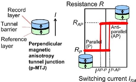
Magnetic memories are based on the magneto-resistive effect in thin films. The spintronic devices are typically composed by a Magnetic Tunnel Junction (MTJ), consisting of thin tunnel barrier sandwiched between two magnetic layers in series with an access transistor as shown in Figure 1. 8.
Figure 1. 7 : Basic structure of FeRAM cell. The crystal structure of ferroelectric material and the polarization-electric field hysteresis curve are also shown. Reprinted from [31]
Figure 1. 8 : Basic schematic of MJT device with resistance switching current characteristics. Reprinted from [5]
- 9 -
The two ferromagnetic layers play different roles: one is a “recording” layer, with reversible magnetization direction, and the other is a “reference” layer, with fixed magnetization direction [34]. The resistance level of the memory cell is determined by the magnetization direction of the recording layer, while the tunneling current depends on the mutual orientation of the magnetic polarization in the two electrodes. The low resistance state corresponds to the parallel state, and the high resistance state corresponds to the anti-parallel state. The very fast programming/read time (<10ns), the very high endurance (>1016) and the non-volatility that strongly reduces the power consumption, make the magnetic memories a serious candidates for SRAM replacement [5]. Nevertheless, magnetic memories still have some challenges to be met such as large cell size, very small memory window, complexity of multilayered metal stack and compatibility with CMOS backend processing without degradation of the magnetic properties of the materials.
1.4.3 Phase change memories
Among the emerging memories, Phase Change Memory (PCM) demonstrated the capability to enter the memory market and to be a mainstream memory for the next few years [35], [36]. PCM memories are based on chalcogenide materials: an alloy of Germanium–Antimony–Tellurium (GeSbTe or GST) is commonly used as active layer in the memory stack (see Figure 1. 9). GST material was largely used in rewritable DVDs. PCM is currently the most mature emerging memory technology.
Figure 1. 9 : (a) Schematic of the PCM cell. (b) Programming schemes of a PCM. Reprinted from [37]
- 10 -
GST material can be switched by means of current flow through the material between an amorphous state and a crystalline state corresponding to the high resistance state and low resistance state, respectively. During “Set” operation (memory programmed to the low resistance state) an electrical pulse is applied to heat a part of the active region (in contact with the “heater”) above the crystallization temperature. During Reset operation, high current and fast pulses (10–100 ns) are required compared with Set conditions to melt-quench the active chalcogenide material and to program the cell to high resistance state as shown in Figure 1. 9-b. The high programming current required during Reset and considered as one of the main challenges of PCMs could be reduced by scaling down the device area, since PCM is programmed by Joule heating [38]. Superlattice-like structure (SLL) based on a super-lattice of thin chalcogenide layers with different compositions, has been proposed as a solution to strongly improve PCM performances in terms of switching speed and programming current (possibility to Reset without melting) [39].
Finally, PCM is very promising to be used as SCM to fill the gap between DRAM and NAND flash. In addition many companies have already produced high density PCM memories based on advanced technology nodes such as Samsung, Hynix, Micron and Intel [22], [36], [40].
1.4.4 Resistive Random Access Memories (RRAMs)
Resistive RAMs are based on resistive switching occurring in Metal-Insulator-Metal (MIM) structure. Structural modifications, mainly the formation and rupture of a conductive path in the active oxide material under applied electric field, lead to memory resistance change between low resistance state (LRS) and high resistance state (HRS), corresponding to the logical states “1” or “0”. Materials used in binary metal-oxide based RRAM are CMOS compatible and could be integrated easily in the BEOL with advanced-node CMOS technologies [19]. The type of defects involved in the creation of the conductive filament (CF) determines if the RRAM is an oxygen vacancy RAM (OxRAM) or metal ions based conductive bridge RAM (CBRAM). RRAM devices could be also categorized by means of switching polarity as “unipolar” RRAM or “bipolar” RRAM as shown in Figure 1. 10.
- 11 -
Unipolar devices: The switching between LRS and HRS and vice versa is obtained by using an electric field with the same polarity but different amplitude. The thermal effects during Reset (switching to HRS) pulses have been proposed as the reasons behind species diffusion resulting in a self-accelerated dissolution of the CF [41] [42].
Bipolar devices: The Set/ Reset operations depend on the polarity of the applied electric field. If Set operation occurs in one polarity, inverse polarity is mandatory to perform the Reset operation. Bipolar devices are more popular in research topics compared to unipolar devices.
The electrode materials and the symmetry of the device structure determine the polarity of RRAM devices as presented in Table 1. 1. By combining the same active oxide material with different top and bottom electrodes, RRAM shows different polarities.
Figure 1. 10 : (a) Schematic of RRAM MIM structure, (b) Schematic of I-V characteristics of unipolar RRAM, (c) Schematic of I-V characteristics of bipolar RRAM. Reprinted from [19].
Table 1. 1 : Different electrodes combinations and their corresponding switching modes. Reprinted from [19]
- 12 -
1.4.4.1
Resistive switching mechanism
The switching mechanisms, corresponding to the creation/rupture of oxygen-vacancies or metal-ions rich conductive filament, include three main operations: Forming, Reset and Set as shown in Figure 1. 11.
Forming: Fresh devices have very large resistance values and often need to be initialized before stable resistive switching mechanisms can be achieved later. Forming operation is required once during the RRAM lifetime. After Forming, RRAM device is in LRS, where a CF connecting the top and bottom electrodes is created. Forming operation is a soft breakdown of the oxide material controlled by compliance current. The latter is imposed using external devices, in most cases a CMOS transistor to avoid permanent damage of the oxide material. LRS value is determined by the compliance current imposed during Forming/Set operations. During Forming operation, higher voltages are required compared with normal resistive switching conditions. Many studies have been focused on possible solutions to design “forming-free” devices by acting on several parameters (e.g. oxide materials, oxide thickness, electrodes materials, fabrication process conditions etc.)[44]–[46].
Reset: Partial dissolution of the CF occurs during Reset, the RRAM device switches to its HRS. Different physical mechanisms have been investigated to explain the Reset process, such as thermal dissolution of the conductive filament for unipolar devices, ion migration for bipolar devices as well as electrode/oxide interface properties that can determine the atomic behaviors during RRAM operations [47]– [49]. The main fundamental issue of resistive switching is the inability to heal the Figure 1. 11 : Schematic of as-fabricated RRAM (initial state), (1) forming operation, (2) Reset operation and (3) Set operation. Reprinted from [43]
- 13 -
total filament during Reset. Uncontrolled residual CF, (e.g. different length, density or shape), remains in the active layer after every Reset cycle. This leads to much higher HRS current (IHRS) compared to pristine state current and to high HRS variability. Cycle to cycle and device to device variability is considered as the weakest point of RRAM technology.
Set: It is similar to Forming operation, but lower applied voltage is required to restore the CF that was ruptured during Reset operation. After Set operation the RRAM is programmed to LRS and could be subsequently switched several times between the two resistance states (HRS and LRS). The memory window is defined as HRS/LRS factor.
1.4.4.2
Conductive bridge RAM (CBRAM)
CBRAM is based on creation and rupture of metal-ions rich CF in the active layer (see Figure 1. 12). The memory structure typically consists of a solid electrolyte layer, that could be a chalcogenide (e.g. GeS2, GeSe) or binary metal-oxide material (e.g. ZrOx, GdOx, TaOx) [50], [51].
The active layer is sandwiched between two metal electrodes, one of which is an electrochemically active (e.g. Ag or Cu) and the counter electrode is electrochemically inert (e.g. W or Pt). Under applied electric field, metal ions are Figure 1. 12 : I-V characteristics of an Ag/GeSe/Pt electrochemical metallization cell with schematics of the formation and rupture of the metallic-rich CF. Reprinted from [52]
- 14 -
generated at the active electrode and driven in the solid electrolyte layer to form a metallic-rich CF, which makes the memory resistance dropping to LRS. During Reset operation an opposite applied bias compared to the one applied for Set operation leads to back-migration of the metal-ions toward the active electrode and the rupture of the metallic CF, thus the memory resistance increases to HRS.
1.4.4.3
Oxide based RAM (OxRAM)
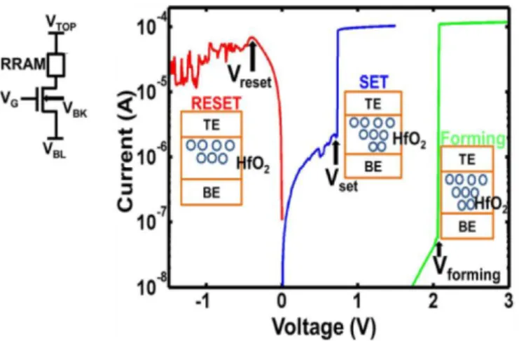
OxRAM is also based on resistive switching with creation and rupture of an oxygen vacancy-rich CF. The device structure consists of a thin layer of binary metal-oxide sandwiched between two metal electrodes. One electrode plays the role of oxygen reservoir, accommodating oxygen ions coming from the active layer during Forming/Set operations. Energy delivered to the device during Forming/Set processes should be controlled to avoid the irreversible breakdown of the oxide. In most cases, a transistor is adopted to control the current through the RRAM structure (1T1R) during programming operations, as shown in Figure 1. 13. The most common binary metal oxide used as active layer in OxRAM devices are HfOx, TiOx, TaOx and AlOx.
OxRAMs have very interesting properties, such as simple MIM structures, multilevel capability thanks to the large memory window compared to STT-MRAM, very good scalability down to 10x10nm2 [53], low operating voltages, fast switching (~10ns and less)[54] .
Figure 1. 13 : 1T1R schematic with typical I-V characteristics of forming, Set and Reset operations with current control for HfO2 based OxRAM. Reprinted from [55]
- 15 -
1.4.5 RRAM key performances and reliability
In this thesis, we will focus on oxide based RAM (OxRAM) devices, we will study their reliability, performances and possible applications. For this purpose, we will review in this section the performances and the improvements of OxRAM devices presented in the literature. In the next chapters, we will present the results that we have obtained and contributions of this Ph.D. thesis to RRAM research field.
1.4.5.1
Uniformity
One of the main issues of OxRAM devices is the resistance variability, for both, cycle to cycle and device to device. The origin of this variability could be attributed to the stochastic nature of the conductive filament, as demonstrated in [56]. HRS variability comes from the variation in the tunneling gap distance created after the rupture of the CF during Reset operation. The HRS variability is most severe compared to LRS variability. Different methods, mainly materials engineering, have been proposed in the literature to improve the uniformity of OxRAM devices. One method is to introduce a thin Al buffer layer between the active oxide layer (HfOx) and the electrode, which leads to a more controllable CF formation [57] (see Figure 1. 14).
Another method to improve uniformity is to confine the region of the CF paths by reducing the cell area [58]. Scaled devices show better cycle to cycle and device to device uniformity compared with larger size devices. Programming solutions have Figure 1. 14 : HRS and LRS distributions, with and without Al layer. Uniformity improved with the presence of Al thin layer. Reprinted from [57]
- 16 -
also been proposed to reduce parameter fluctuations, such as ramping up the Reset voltage, using multiple pulses instead of single programming [59].
1.4.5.2
Endurance
Programming endurance of OxRAM devices depends on many factors, such as programming conditions, device structure, process conditions, materials etc. The endurance failure could occur in both directions: LRS fails toward HRS or HRS fails toward LRS, as shown in Figure 1. 15.
LRS failure is attributed to degradation of the oxygen vacancies (Vo) mobility in the CF constriction due to high local temperature during switching [61]. It is sometimes attributed to the formation of an oxide layer between the electrode and the active oxide layer [62]. HRS failure is most common. Usually, after cycling, the OxRAM devices are stuck in LRS without possibilities to Reset the device again. HRS failure was attributed to different scenarios: (1) too many Vo generated at, or near, the electrode/oxide interface; (2) too many Vo generated in, or near, the CF; or (3) too many Vo generated inside the HfO2 matrix [19]. Excellent endurance (>1015) is required for RRAM devices to replace existing memory technologies (e.g. DRAM). H. Y. Lee et al. demonstrated an endurance over 1010 cycles for HfOx-based OxRAM using optimized programming conditions and CMP to flatten the memory bottom electrode [63].
1.4.5.3
Data retention
Ten years data retention at up to 85°C is expected for nonvolatile memories. Deep understanding of the resistive switching mechanisms is required to improve
- 17 -
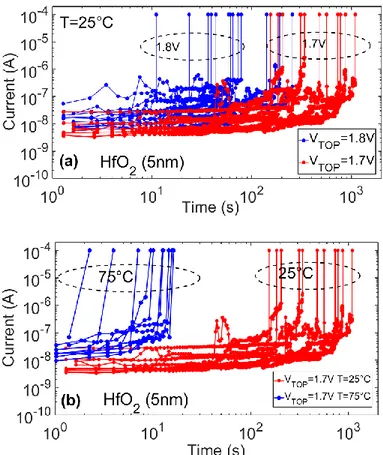
OxRAM data retention. Many groups have investigated the data retention of OxRAM devices at microscopic levels. In [64], two possible retention degradation mechanisms were identified in HfO2/Hf based OxRAM: (1) the oxygen diffusion from the oxygen scavenging layer and recombination with Vo; (2) the Vo diffusion out of the CF and dissolution of the CF (see Figure 1. 16). They suggested an additional full stack annealing after RRAM cell fabrication to limit oxygen diffusion from the scavenging layer, because of the bonding of free oxygen with Hf electrode to form HfOx. This method will reduce the mobile oxygen supply. The compliance current imposed during Forming/Set operations has an important effect on data retention. With higher compliance current the CF is more stable, therefore, LRS shows batter data retention.
In [55], the impact of atomic composition on data retention has been investigated by means of ab initio calculations. LRS retention failure was attributed to the lateral diffusion of oxygen vacancies at the constriction/tip of the conductive filament in HfO2-based RRAM. Al incorporation in HfO2 was found to improve the data retention thanks to shorter bond associated with higher atomic concentration and higher Vo diffusion barrier in Al doped devices. H. Y. Lee et al. demonstrate 500 minutes data retention for TiN/HfO2/Ti device at 200°C [65].
In the next chapter we will present our work on different methods to incorporate Al in HfO2 based OxRAM, and their effects on data retention and forming voltage.
1.4.5.4
Programming speed
The major issue of nowadays memory hierarchy is the speed gap between main memory (e.g. DRAM) and storage (e.g. NAND Flash). Emerging non-volatile
- 18 -
memories should provide high programming speed (in the order of 10’s of ns) comparable to DRAM and SRAM, and high density and non-volatility, comparable to NAND flash. Elisa Vianello et al. [54] demonstrated a switching time lower than 10ns for HfO2/Ti based OxRAM as shown in Figure 1. 17.
Programming speed strongly depends on the binary metal-oxide material, and the programming conditions. In [19], high switching speed compared to DRAM is demonstrated for OxRAM devices using different metal oxide materials (see Table 1. 2 ).
1.4.5.5
Irradiation immunity
NVMs are used in a variety of space applications. Memories based on charge storage, such as flash memory, are not radiation hard technologies [66], as charges are sensitive to radiations. RRAM devices seems to be promising for space applications because this memory technology does not depend on charge storage but Figure 1. 17 : Programming time versus voltage for HfO2/Ti based OxRAM. Reprinted from [54]
Table 1. 2 : Programming speed of OxRAM devices with different oxide materials. Reprinted from [19]
- 19 -
rather on resistive switching mechanism, based on creation and rupture of oxygen vacancies-rich CF. Recent works show no direct effects of heavy ions irradiations (focusing on Single Event Effects - SEE) on devices using TaOx or Hf/HfO2 stacks. The observed phenomena were either due to the degradation of the access transistor or to single events effects in the control circuitry [67]. In the next chapter, we will present our experimental and simulations results on HfO2 based RRAM irradiation immunity. The memory devices show irradiation hardness under very energetic ions strikes.
1.5 Emerging memories architectures
1.5.1 3D Cross point architecture
In memory systems, the memory devices are organized in arrays. Every memory device in the array shares with neighbors one of the addressing lines. Cross-point architecture consists on the implementation of the two-terminal memory device on the cross-point between two perpendicular metal lines called “wordline” and “bitline” as shown in Figure 1. 18-a. In cross-point architecture the effective cell area could achieve 4F², considering the width of the metal line and the space imposed between two metal lines are equal to “F” where “F” is the minimal feature size. 4F² is the smallest cell footprint that could be achieved from layout point of view. It is possible to stack multiple 2D cross-point layers into 3D stacked cross-point architecture, as shown in Figure 1. 18-b.
Figure 1. 18 : Schematic of (a) 2D cross-point array, (b) Stacked 3D cross-point array. Reprinted from [68].
- 20 -
If 3D stacked cross-point architecture is adopted, the minimal effective cell area is reduced to 4F²/n, where n is the number of 2D stacked layers. 3D cross-point is considered as very promising architecture for high density emerging resistive memories.
1.5.2 VRRAM architecture
A practical problem associated with stacked 3D cross-point array is that the cost per bit does not always scale with the increasing number of layers. This architecture requires critical process steps, e.g., lithography and etching of metal lines and via contacts for each additional layer [69]. For 3D vertical NAND architecture a single critical lithography and etching step are required to define the memory cells and multi-layers are formed simultaneously. Vertical Resistive-RAM (VRRAM) architecture was proposed for cost effective data storage application [70], [71]. VRRAM is expected to consume less than 1/3 in lateral and 1/2 in vertical dimension compared to the current charge trap based VNAND, which is promising for further reducing the cost per bit [69]. Figure 1. 19-a shows a schematic of VRRAM architecture and the active zone where the resistive switching occurs between the vertical and horizontal electrodes. Two memory points are identified at the same horizontal level between two parallel horizontal electrodes (see Figure 1. 19-b).
1.5.3 Sneak path current issue in RRAM arrays
The capability to address efficiently a specific cell within an array for reading or programming, without interfering with other cells, is as important as the basic Figure 1. 19 : (a) Schematic of VRRAM architecture, (b) Schematic of a memory point (one unit) with 2 RRAM devices in VRRAM architecture. Reprinted from [70], [71]
- 21 -
performances of the storage element. Each memory cell in the array should have high selectivity that could be provided by non-linear electrical characteristics of RRAM devices. However, the majority of the reported RRAM devices show almost ohmic characteristics (linear) in LRS and HRS states, consequently, this leads to “Sneak path current” issue through the unselected cells in the memory array. Sneak path current causes read and programming degradations, it also rises the total power consumption in the memory array.
Figure 1. 20 shows half bias scheme during programming phase of a selected cell in the memory array. Programming bias and zero bias are applied on the word line and bit line of the selected cell respectively, half programming bias is applied on unselected word lines and bit lines. With the presence of sneak-path currents coming from half selected cells, the readout signal on the selected bit line does not correspond to the pure current through the selected cell, thus a read error occurs and higher power is consumed during the memory operation. In the next section we will review the selector devices that have been proposed to get rid of sneak path current issue in memory arrays.
1.6 Access devices for RRAM arrays (selectors)
The use of selector devices with non-linear I-V characteristics in selector one-resistor structure (1S1R) is proposed to suppress the sneak-path currents in RRAM Figure 1. 20 : (a) Schematic of cross-point array illustrating the selected cell (red cube) and the leakage currents through the unselected/half-selected cells (blue cubes). (b) Schematic of the circuit of cross-point array. Green line: selected cell read current, red lines: sneak-path currents. Reprinted from [69].
- 22 -
arrays. The high resistance of the selector at low bias is the dominant characteristic of half-selected or non-selected memory devices in the array, this results to suppression of the parasitic current as shown in Figure 1. 21.
1.6.1 Requirements for access devices
An access device must satisfy a number of specifications to be suitable for the integration in high density cross-point arrays. Selector characteristics could be summarized as following:
1. Two terminal device
A simple two terminal structure is required for selector devices to avoid extra cell area that prevents achieving the minimal effective cell area of 4F². As an example, the three-terminal transistor can provide perfect selector performances for sneak-current suppression, but at the cost of complex process and large area of single cell. 2. High ON-state current density
A selector device should be able to deliver enough current density to program (Set/Reset) the memory element. Selector’s ON-current density must be in the order of several MA/cm². In the case of a 100nm² cell area that should be programmed at least with 10µA as compliance current, a current density of ~10MA/cm² is required. 3. Low OFF-state leakage current (high selectivity)
Figure 1. 21 : (a) Schematic of leakage current suppression in the case of 1S1R structure, (b) electrical characteristics comparison between 1R with ohmic behaviors and 1S1R with non-linear characteristics. Reprinted from [69].
- 23 -
The maximum cross-point array size is linked directly to the circuit performance, such as read/write margins and power consumption. These performances are strongly related to the amount of leakage current flowing through the unselected cells in the cross-point array [72], [73]. Off-state current should be several orders of magnitude lower than On-state current to improve the overall array operation and to allow the implementation of large arrays. Consequently, high selectivity increases the overall area efficiency [74].
4. Bidirectional operation
Most of the reported RRAM devices exhibit bipolar characteristics during programming operations (Set/Reset). A selector device that provides current flowing in opposite polarizations is required in conjunction with bipolar emerging memories. In addition, high On-current density and high selectivity are required in both polarities.
5. Voltage compatibility with the memory cell
RRAM memory elements have different programming voltages (Set/Reset) depending on their material compositions. Voltage compatibility between the selector and RRAM cell is required in order to transfer selector selectivity to the 1S1R full cell. If the switching voltage of the access device is much lower compared to storage element, the leakage current through the half-selected cells will be high enough to disturb read and program operations in the memory array.
6. Process compatibility
The access device technology must be CMOS compatible, therefore materials such as Au, Pt etc. should be excluded from the selector structure. For 3D multilayer integration, the selector device has to be compatible with the thermal budget of the back end of the line (BEOL) process. This enable stacking subsequently multiple memory layers with interconnections among them.
The selector characteristics should never limit the memory array performances and reliability. Therefore, any other performances of the access device (e.g. switching speed, endurance, uniformity etc.) must be identical or better than the performances of the storage element.
Based on the above requirements it is very challenging to find the ideal access device that could provide all the characteristics needed for high density memory arrays. In the following, we will summarize the main candidates that have been proposed in the literature as selectors for 3D cross-point architectures.
- 24 -
1.6.2 Types of selector devices
1.6.2.1
Si-based selectors
Three terminals Si based transistors are considered as one of the best access devices for RRAM cells in terms of high current drive, high selectivity, current compliance, high reliability, bidirectionality mode etc. However, transistors require large area and complex process compared to two terminal selectors. Moreover, high thermal budgets are needed which is incompatible with 3D multilayers BEOL stacking [74]. Vertical Si PN junction deposited by selective epitaxial growth (SEG) on crystalline Si substrate was proposed as selector for unipolar PCM. The cell size was 5.8F² for the 90nm technology node. High ON-current was demonstrated (>25MA/cm²) with selectivity about 108 [75]. For bipolar emerging memory technologies, Si based NPN diodes are proposed as access devices (see Figure 1. 22-a). These devices provide ON-current density >1MA/cm² and selectivity > 250 or > 4700 with respect to voltage polarities as shown Figure 1. 22-b [76] .
The proposed Si based diodes are fabricated using epitaxial growth [75], [76], that is well known by its high temperature (~700°C) according to the crystallization Figure 1. 22 : (a) Schematics of NPN selector with its band diagram at different polarizations, (b) |J|−V characteristics for 1/3 polarization scheme of the NPN junction in linear (left axis) and log scale (right axis). Reprinted from [76]
- 25 -
temperature of Si. The high process temperature required for Si based diodes are not compatible with BEOL process, therefore such access devices are not suitable for 3D multilayer stacking.
1.6.2.2
Oxide based PN diodes
Many groups proposed the oxide based PN junction as access devices for unipolar memories in cross-point arrays [77]–[81]. I. G. Baek et al. presented a PN junction diode using NiO as p-type and TiO2 as n-type semiconductor with process temperature below 300°C. The current density provided by the junction was very low (~1KA/cm²), thus not compatible with unipolar RRAM programming current requirements (>1MA/cm²) [79]. Myoung-Jae Lee et al. presented a p-CuOx/n-InZnOx heterojunction oxide diode as access device for unipolar NiO based RRAM, higher current densities were demonstrated (~10KA/cm²) compared with p-NiOx/ n-TiOx junction. However, this current density still very low for the programming of targeted memory technologies [80]. Seung-Eon Ahn et al. built a one-time field-programmable (OTP) memory with Al2O3 as binary oxide material for the memory cell and a p-n CuO/InZnOx diode as access device [81].
1.6.2.3
Oxide tunnel barriers
One approach to obtain non-linear I-V characteristics is to introduce a thin oxide tunnel barrier in the memory stack. Several high-K materials have been reported for this purpose (HfO2, TiO2, Al2O3 and SiO2) [82]–[86]. In [85], Al2O3 tunnel barrier was used with 5 x 6 µm² HfO2 based RRAM, this method provided a selectivity of ~37. The selectivity is defined as the ratio between the current at the read voltage (I @ Vread) and the current at half or one third read voltage, with respect to the adopted polarization scheme during read/programming operations (half bias or 1/3 schemes). The current conduction in the tunnel layer (Al2O3 in this case) is dominated by Fowler Nordheim tunneling, which is well known being described by a non-linear (exponential) current conduction mechanism. Seong-Geon Park et al. [84] reported an RRAM device based on double layers of Transition Metal Oxide (TMO) and two tunnel barriers at top and bottom as shown in Figure 1. 23. This structure provided a selectivity of ~17.
- 26 -
B. Govoreanu et al. [87] reported a self-compliant RRAM consisted of TiO2 switching layer and Al2O3 tunnel barrier as shown in Figure 1. 24. A selectivity of ~100 and ON-current density of 0.1 MA/cm² were measured for this device.
Figure 1. 23 : (a) (b) Schematics of RRAM structure with and without tunnel barriers. (c)(d) Linear and non-linear characteristics of RRAM device. Reprinted from [84]
Figure 1. 24 : TEM cross-section of the full RRAM stack with Al2O3 tunnel barrier, and the corresponding I-V characteristics. Reprinted from [87]
- 27 -
The oxide tunnel barrier is fully compatible with BEOL process requirements. However, this approach suffers from low selectivity that is strongly required to implement large memory arrays.
1.6.2.4
Mixed Ionic Electronic Conduction selector (MIEC)
Mixed ionic electronic conduction (MIEC) occurs when the material conducts ions and electronic charges. Access devices based on MIEC materials have become an attractive choice for 3D cross point arrays. In [88]–[90] copper-containing MIEC material is reported as selector device. Typically, the MIEC material is sandwiched between two electrodes where at least one must be inert or non-Cu-ionizing. The applied voltage leads to a transient Cu ion movement, followed by a steady electron/hole diffusion current which translates into non-linear I-V characteristics as shown in Figure 1. 25. The large fraction of mobile Cu enables very high current densities.
MIEC materials are BEOL-friendly with process temperature <400°C. They provide high current density (>10MA/cm²) and high selectivity with very low leakage in the voltage range between 0 and ~1.5V (leakage below 10nA), as shown in Figure 1. 25. With low current operation regime (<10µA), the MIEC can provide more than 1010 endurance cycles. However, with high current operation (>10µA), a voltage margin degradation occurs and the selector becomes a short circuit before 106 endurance cycles [89], [90]. Endurance failure is explained by the accumulation of Cu ions in the MIEC material. In addition, MIEC selector has small operating voltage range Figure 1. 25 : Schematic of a MIEC selector structure and its I-V characteristics. Vm (Voltage margin) corresponds to the voltage difference for reaching 10nA at positive/negative polarities. Reprinted from [89], [90].
- 28 -
(low voltage margin). This feature makes the MIEC materials less suitable as access devices for RRAMs that require relatively high programming voltages compared to the operating voltages of MIEC.
1.6.2.5
Threshold switching selectors
Access devices with threshold switching characteristics are considered as very promising candidates for 3D cross-point arrays. A threshold switch consists of two main regimes: (i) a very high resistance state at low field that serves to suppress the sneak-path current, (ii) a very low resistance state with high current drive when the applied bias exceeds a threshold voltage, this serves for RRAM programming. Different types of devices with threshold switching characteristics are proposed as access devices for 3D cross-point memory arrays. In this section, we will review some of the proposed threshold switching devices.
1) Ovonic threshold switching (OTS)
Ovonic Threshold Switching (OTS) principle was first observed by S. R. Ovshinsky in various thin film chalcogenide materials [91]. As demonstrated in Figure 1. 26 the I-V characteristics show abrupt decreasing from high initial resistance state to low resistance state when the applied voltage matches the threshold voltage “Vth”. The device remains in the low resistance state if a minimum holding voltage (“VH” Figure 1. 26 : I-V characteristics of the threshold switching in OTS material with the presence of a series resistance that determines the load line. Reprinted from [92]
- 29 -
in Figure 1. 26) is applied, otherwise the OTS device switches back to the high resistance state. Therefore, the threshold switching principle is volatile in this case. The attractive characteristics of OTS based access devices could be summarized as follows:
1) High selectivity
2) A large off-state margin that ensures the selectivity of the full 1S1R during reading and programming.
3) The capability to deliver high current density in the low resistance state (> 10MA/cm²).
The OTS mechanism was explained by different theories, such as mixed electronic and thermal (MET) model, which is a thermally induced electronic switching [93]. It was also explained by field-induced carrier generation [94], (i.e. when all the traps are filled, carriers can transit the sample with an enhanced mobility and the generation rate required to keep the traps filled is reduced from its threshold value). Daniele Ielmini [95], demonstrated an analytical model based on the balance between electron energy gain and relaxation in the hopping transport. The I-V characteristics in the low current regime are described by the Poole-Frenkel (PF) current conduction mechanism, and the exponential increase of the current is described by the field-induced barrier lowering effect, which enhances electron hopping conduction as shown in Figure 1. 27.
Figure 1. 27 : (a) Measured I-V for a PCM with Ge2Sb2Te5 chalcogenide and simulated curves for different values of the amorphous chalcogenide thickness, (b) Schematic of conduction bands in the low and high voltages regimes. Reprinted from [95]
- 30 -
As the applied voltage further increases, the electrons tunnel to higher energy traps. The tunneled electrons occupy the shallow traps close to the conduction band, giving rise to a non-uniformity of the electric field across the OTS material. To a certain extent, the region near the cathode becomes ‘invisible’ for the tunneling electrons. This corresponds to the occurrence of the S-type I-V snapback and then the OTS switching happens.
Different chalcogenide materials were reported for binary OTS access devices such as ZnTe, GeTe, SiTe, GeSe etc. [96]–[98]. In [99] Myoung-Jae Lee et al. demonstrated an AsTeGeSiN based OTS selector successfully integrated with TaOx based RRAM, as shown in Figure 1. 28. The selector provides 11MA/cm² as ON-current density, a selectivity of 1000 for 30x30nm2 cell size and more than 108 endurance cycles. Post deposition annealing could reduce the off-state leakage current as the trap density in the chalcogenide alloy decreases after annealing [99]. DerChang Kau et al. [100] demonstrated a 1S1R cell with phase change memory (PCM) as storage element and OTS selector. The single cell provides 9ns programming speed and 106 endurance cycles.
Chalcogenide materials are very promising candidates for access devices implementation. The characteristics of the alloy strongly depends on its material composition (e.g. elements concentration), therefore, most of the research today is focusing on chalcogenide materials engineering to obtain the optimal OTS based selector. In chapter IV, we will present our 1S1R device with HfO2 based RRAM as storage element and GeSe based OTS selector.
Figure 1. 28 : TEM image of the 1S1R device structure with AsTeGeSiN based OTS and the corresponding I-V characteristics. Reprinted from [99]
- 31 -
2) Metal Insulator Transition devices (MIT)
Metal-Insulator-Transition devices present a “fast” reversible resistivity changes between low and high resistance states that is thermally triggered. MIT mechanism is widely observed in condensed-matter systems, such as VO2, NbO2 etc. [101]. Myungwoo Son et al. [102] presented Pt/VO2/Pt selector (see Figure 1. 29). VO2 based selector provides a selectivity >50, fast switching speed (<20ns) and high ON-current density (>1MA/cm²). Electrical characteristics of the presented VO2 based access device strongly depend on the device size, as the MIT mechanism is observed only for small devices (nanoscale) while large area devices (microscale) show Ohmic characteristics, as shown in the left inset of Figure 1. 29. However, the operation temperature of VO2 is very low (<67°C). Therefore, such as access device is not compatible with applications that require operating temperatures up to 85°C. Seonghyun Kim et al. [103] reported Pt/NbOx/Pt as MIT access device with high temperature stability (~160°C) compared to VO2. However, the device shows higher switching voltages and low selectivity as shown in Figure 1. 30.
Figure 1. 29 : I-V characteristics of VO2 based MIT selector with 250 nm active area (via diameter). Inset on the left: I-V characteristics of microscale device (300 x 300 µm²). Inset on the right: schematic of the nanoscale selector device. Reprinted from [102]
- 32 -
The main issue of MIT based selector is the high current level in the OFF-state. This leads to high leakage current in 3D cross-point arrays during read/programming operations. The high current level in the OFF-state seems to be mandatory such device to produce enough Joule heating to trigger the transition between Metal and Insulator phases.
3) Field Assisted Super-Linear Threshold (FAST) selector
Sung Hyun Jo et al. [104] reported a Field Assisted Superlinear Threshold (FAST) selector. I-V characteristics are very similar to volatile threshold switching (e.g. OTS), but with much better performances (see Figure 1. 31). The selector device shows a selectivity around 1010, 5MA/cm² as ON-current density, and 108 endurance cycles. The 1S1R shows a selectivity of ~106. The processing temperature of a FAST selector is less than 300°C, therefore, it is compatible with 3D-cross point integration process. As a consequence, FAST selector shows excellent characteristics that are suitable for high memory density integration. Unfortunately, the material composition of this selector is still a confidential work to Crossbar company.
Figure 1. 31: I-V characteristics of (a) RRAM (b) FAST selector (c) 1S1R device (d) crossbar array based on 1S1R. Reprinted from [104]
- 33 -
1.6.3 Selectors benchmarking
Selector device ON-current density (MA/cm²) Selectivity Endurance#cycles Polarity Comments
Si
transistor >1 >106 >108 Bipolar
Complex process and large device area therefore, not suitable for 3D integration
Oxide
diode ~10 >105 >104 Unipolar
Not suitable for bipolar emerging memories
Si NPN
diode >1 >240 ---- Bipolar
Process complexity and low selectivity
Tunnel
barriers <1 <100 ---- Bipolar Low performances a-Si
barrier >1 ~103 ~106 Bipolar
High operating voltage required
MIEC >10 >105 >106 Bipolar
small operating voltage rang (low voltage margin), limited endurance
OTS >10 >104 >108 Bipolar Complex materials
FAST >1 >105 108 Bipolar Material not identified
- 34 -
1.7 Thesis content overview
1.7.1 Thesis objectives
The integration of embedded Flash memories with advanced CMOS nodes poses many problems in terms of process compatibility and physical limitations of the memory device itself. To realize high-density storage memories, single cells should provide specific characteristics (e.g. high selectivity, low power consumption, ultra-scaled devices etc.) high performances and excellent reliability.
Many types of emerging memories such as phase change memories (PCM), magnetic memories (MRAM) and resistive switching memories (RRAM) are proposed as candidates for embedded memories and SCM applications.
In this thesis, we will investigate first the reliability of HfO2 based RRAM. To improve the data retention of these devices and make them compatible with high temperature environments such as automotive applications, we propose different material engineering strategies. In addition, we investigate the effects of heavy ions irradiation on HfO2 based RRAM for space applications, where the electronic devices should provide high levels of radiation immunity in such environments.
Crossbar architecture targets the storage class memory (SCM) applications. After the single cell reliability study, we will investigate the compatibility of HfO2 based RRAM with high density cross-point architectures. For this purpose, we introduce first an additional tunnel barrier to the memory stack, resulting in a Self-Rectifying (selector-less) Cell (SRC), then we will integrate a two-terminal OTS selector device with the RRAM element in 1S1R device. We will explore the characteristics and the performances of both access devices.
1.7.2 Thesis outline
This thesis is organized as follow:
Chapter 2: Characterization and modeling of HfO2 based RRAM cells
In this chapter, we introduce our HfO2 based RRAM technology, describing the process and device structure details. The device characterization methodologies and
- 35 -
the measurement equipment that we have used during this Ph.D. are presented in details as well. Finally, we present the simulation tool that we adopted to investigate the kinetics of the forming process, the charge transport mechanisms and defects generation in the binary oxide material at the microscopic level.
Chapter 3: Reliability of HfO2 based RRAM cells
In this chapter, we investigate first the data retention of the HfO2 based RRAM. Then, we propose aluminum (Al) incorporation with different methods to improve the data retention of the memory cells. The effects of Al incorporation on the forming process have been investigated at the microscopic level by means of physics based simulations. Then, we will study the radiation immunity of the RRAM devices by irradiating the memory cells with heavy ions comparable to those existing in the space. The experimental results obtained after irradiation are also explored by simulation.
Chapter 4: Access devices for cross-point memory arrays
In this chapter we investigated two technologies to fabricate a back-end selector for crossbar architectures. First, we introduce a tunnel barrier to the HfO2 based RRAM, this method shows limited performances (e.g. low selectivity). Then, we integrate an OTS access device in series with the memory cell. A detailed investigation of the main memory operations, Forming, Set, Reset and read is presented. An innovative reading strategy is proposed to decrease power consumption during read process. The 1S1R shows better characteristics in terms of selectivity compared to the tunnel barrier solution. In addition, we present an OTS material engineering to improve the selectivity of the 1S1R device.
Chapter 5: Summery and perspectives
In the conclusion, we will summarize the main results and contributions of this Ph.D. In addition, we provide a perspective on the future work that needs to be done for the further progress of RRAM reliability and novel access devices.