HAL Id: lirmm-00989717
https://hal-lirmm.ccsd.cnrs.fr/lirmm-00989717
Submitted on 17 Dec 2020
HAL is a multi-disciplinary open access
archive for the deposit and dissemination of
sci-entific research documents, whether they are
pub-lished or not. The documents may come from
teaching and research institutions in France or
abroad, or from public or private research centers.
L’archive ouverte pluridisciplinaire HAL, est
destinée au dépôt et à la diffusion de documents
scientifiques de niveau recherche, publiés ou non,
émanant des établissements d’enseignement et de
recherche français ou étrangers, des laboratoires
publics ou privés.
3D Design For Test Architectures Based on IEEE P1687
Yassine Fkih, Pascal Vivet, Bruno Rouzeyre, Marie-Lise Flottes, Giorgio Di
Natale, Juergen Schloeffel
To cite this version:
Yassine Fkih, Pascal Vivet, Bruno Rouzeyre, Marie-Lise Flottes, Giorgio Di Natale, et al.. 3D Design
For Test Architectures Based on IEEE P1687. 4th IEEE International Workshop on Testing
Three-Dimensional Stacked Integrated Circuits (3D-TEST), Sep 2013, Anaheim, CA, United States.
�lirmm-00989717�
3D Design For Test Architectures
Based on IEEE P1687
Yassine Fkih(1,2), Pascal Vivet(1),
Bruno Rouzeyre(2), Marie-Lise Flottes(2), Giorgio Di Natale(2), Juergen Schloeffel(3)
(1) CEA-Leti, MINATEC Campus, F38054, Grenoble France (2) LIRMM, Univ Montpellier II/CNRS, Montpellier France
(3) Mentor Graphics, Hamburg, Germany
Abstract—3D stacked integrated circuits based on Through
Silicon Vias (TSV) are promising with their high performances and small form factor. However, these circuits present many test issues. In this paper we propose a novel 3D Design for Test (DFT) architecture based on IEEE P1687. The proposed test architecture enables test at all 3D fabrication levels: pre, mid, and post-bond levels. We discuss 3 DFT architecture proposals and we show one practical implementation using a commercial EDA tool.
Key words: 3D IC, DFT, pre-bond test, post-bond test, JTAG, IEEE 1149.1, IJTAG, IEEE P1687
I. INTRODUCTION
The stacking process of integrated circuits using TSVs (Through Silicon Via) is a promising technology that keeps the development of the integration more than Moore’s law, where TSVs enable to tightly integrate various dies in a 3D fashion. Regarding applications, 3D stacking allows a wide range of new SoC applications, such as heterogeneous stacking (Digital, Memory, RF, Mems); Interposers for multi-chip connection are becoming similar to a silicon board. The first upcoming 3D applications are mainly the WideIO DRAM 3D memory interface for high throughput and low power memory-on-logic stacking [1].
Nevertheless, 3D integrated circuits present many test challenges including the test at different levels of the 3D fabrication process: pre-, mid-, and post- bond tests. Pre-bond test targets the individual dies at wafer level, by testing not only classical logic (digital logic, IOs, RAM, etc) but also unbounded TSVs. Mid-bond test targets the test of partially assembled 3D stacks, whereas finally post-bond test targets the final circuit. It is generally admitted that a 3D test flow [2] should involve test procedures at all stacking levels of the 3D components. In this paper we present a 3D DFT architecture based on IEEE P1687 and auto die-detection mechanism.
The paper is organized as follows. In section II we introduce the state of the art of Design For Test of 3D integrated circuits, in section III we give an overview of the IEEE P1687 standard, in section IV we show three DFT proposals based on IEEE P1687, in section V we show practical implementation of a 3D circuit on a passive
interposer, and in section VI we give conclusions and future work.
II. STATE OF THE ART
Many DFT architectures were proposed for testing 3D integrated circuits. The first papers treated: pre-bond test of 3D processors using scan islands and so called layer test controller (LTC) [3], scan chain optimization approaches [4], and other test issues like test cost optimization [5]. More recent works propose die level wrappers based either on IEEE 1500 [6] or IEEE 1149.1 [7] test standards that allow 3D test at all levels: pre-, mid-, and post-bond. The test architecture has mainly three features: use of dedicated probe pads for non-bottom dies to perform pre-bond die testing, use of “TestElevators” to drive test signals up and down during post-bond test, and use of a hierarchical WIR (Wrapper Instruction Register) chain to configure test interconnects. These features satisfy 3D circuits testing requirements but can be improved to avoid the configuration time of the hierarchical WIR especially for mid-bond and post-bond tests.
On the remainder of this paper, we will propose 3D test architecture proposals based on IEEE P1687 (IJTAG) standard using automatic die-detection mechanism.
III. OVERVIEW OF THE IEEEP1687STANDARD
The main purpose of the IEEE P1687 standard, also called IJTAG, is to develop a methodology for access to embedded test and debug features, via the IEEE 1149.1 Test Access Port (TAP) [8]. This means that in IEEE P1687 JTAG signals (TRST*, TCK, TMS, TDI, and TDO), and JTAG logic including: IR (Instruction Register) and associated decoder, TAP Controller, and DR (Data Registers) are used. Additional logic is added to the JTAG circuitry, in order to enable the access to embedded DFT instruments [9].
In IEEE P1687 it is essentially a Test Data Register (TDR) called Gateway which is added to control embedded instruments dynamically. The configuration is done on 2 steps: the first step is to select the Gateway instruction by shifting its corresponding op-code in the shift-IR state on the JTAG finite state machine [10]. The second step is to configure SIBs (Segment Insertion Bits) by shifting the configuration sequence in the shift-DR state [8,10].
This work was funded thanks to the French national program 'programme d’Investissements d’Avenir, IRT Nanoelec' ANR-10-AIRT-05
There are 4 archetypal types of instruments [8,11,12]: Type-A instrument, also called Simple or
Self-contained does not support a serial path with
simple static signals as input control. An example of this type is a memory BIST (Built-In-Self-Test).
Type-B instrument: 1149.1 compatible or
TDR-Like (Test Data Register), defined to have a single
data register supporting a single TDI-TDO serial chain. An example of a Type-B instrument is any instrument that is directly managed by 1149.1 state-machine signals and associated Select-Capture-Shift-Update protocol.
Type-C instrument : Self-instructed or 1500-like that operates identically to an 1149.1 Compatible 1500-TAM that has multiple internal registers and requires a Select-IR signal; has a serial-scan-path that may have multiple serial-scan-paths or contributors, where one serial-scan-path is a local instruction register. An example of a Type-C instrument is a 1500-wrapped core with core boundary-scan cells that do not require the Transfer signal.
Type-D instrument: is a Type-B or Type-C instrument whose control interface includes at least one 1149.1 non-compatibility: such as a signal that cannot be generated by the TAP controller. An example of a Type-D instrument is a 1500-wrapped core with core boundary-scan cells that do require the Transfer signal.
The IEEE P1687 proposes different types of connectivity schemes between instruments which can be grouped into two categories: hierarchical and non-hierarchical (flat).
Non-hierarchical schemes include: flat, daisy-chain, star, and concatenate.
Hierarchical schemes include: Replace-Parent, Before-Parent, and After-Parent.
In next section, we propose three DFT architectures for 3D circuits based on this test standard which has many benefits including:
Using high level languages ICL (Instrument Connectivity Language) and PDL (Procedural Description Language)
Managing different types of instruments using one common control logic based on the classical JTAG IEEE 1149.1 control logic.
IV. IEEEP1687BASED 3DDFTPROPOSALS
Three DFT architectures based on IEEE P1687 are proposed here:
A. First DFT proposal: One Tap controller in the stack
The first 3D DFT architecture based on IEEE P1687, shown in figure 1, where only the bottom die has IEEE P1687
control logic: classical JTAG logic (TAP controller, instruction register and associated decoder, …) and additional components SIB that control test data registers.
TCK TDI TMS TDO TRSTn TAP Controller SIB T D R SIB T D R SIB T D R SIB T D R SIB T D R SIB T D R SIB T D R SIB T D R SIB T D R
Figure 1. First DFT architecture one TAP Controller in the stack
This architecture is a direct application of the IEEE P1687 standard in 3D context where components of all dies are seen as instruments. As described in III, targeted instruments can be of 4 types. Each die can be considered as an instrument or can contain many instruments: three in this example. TSVs are required to drive IEEE P1687 control and test data signals to upper dies.
This architecture permits the internal test of all instruments in the 3D stack simultaneously or individually by using the IEEE P1687 infrastructure. The added DFT in this architecture is not costly: JTAG logic is added only for bottom die, and control signals are generated to upper dies through TSVs. But it will be possible to perform the test only at post-bond level since all control logic is embedded in the bottom die. One major limitation of this architecture is that the test of inter-die interconnections like TSVs is not possible since boundary-scan cells are generated only in the bottom die to perform the test of external pads.
B. Second DFT architecture: Separate IEEE P1687 dies
The second DFT architecture shown in figure 2 is based on IEEE P1687 standard and also on automatic die-detection [13]. Hereafter a short summary of the automatic die-detection mechanism is given.
1) Summary of automatic-die detection mechanism
The principle of the automatic die-detection is to drive automatically multiplexers of JTAG inputs (TRST*, TCK, TMS, TDI) from pads or TSVs and multiplexer of JTAG output TDO from current die or upper die. This is shown in figure 2, signals colored in red are automatically configured by the mean of 2 die-detectors: one to detect the presence of upper die and one to detect the presence of lower die. Die detectors are not shown in the figure for clarity purpose, but each one is composed of a micro-buffer cell and an associated TSV. The micro-buffer behaves like a normal buffer with an additional pull-down resistance to detect high-impedance.
2) Details of the second DFT proposal
Each die embed IEEE P1687 infrastructure, so able to manage the test of different types of instruments. This can be the case of a 3D circuit composed of stacked System on Chips (SoC), where each die has different components: cores, memories, digital logic … The components of each SoC can be treated as instruments using IEEE P1687 test standard.
TCK TDI TMS TDO TRSTn TCK TDI TMS TDO TRSTn TCK TDI TMS TDO TRSTn TAP Controller SIB T D R SIB T D R SIB T D R TAP Controller SIB T D R SIB T D R SIB T D R TAP Controller SIB T D R SIB T D R SIB T D R
Figure 2. Second DFT architecture: separate IEEE P1687 dies
With this architecture, only JTAG signals are driven to upper dies: control signals (TRST, TCK and TMS) are common for the 3 dies, and data signals (TDI and TDO) are chained serially to form a daisy chain through the 3D circuit. Each die has a full JTAG control logic, so each die is independent from the other. The use of IEEE P1687 standard is local at die level, but simultaneous test is possible when loading Gateway instruction simultaneously in many dies.
With this architecture, all testing levels (pre-, mid- and post-bond) are possible. Pre-bond level is done through pad path which is selected automatically by the mean of die-detectors, and using JTAG and IEEE P1687 infrastructure. Also, all JTAG instructions are permitted including the “extest” instruction which can be used to perform inter-die TSV testing, “intest” to perform internal die testing, and launching the IEEE P1687 Gateway instruction able to configure dynamically many instruments to be tested at the same time or independently.
In term of area overhead of this architecture, each die should embed: JTAG and IEEE P1687 infrastructure, two die-detectors, and some multiplexing logic. In terms of flexibility, this DFT architecture is not flexible, in a way that all dies should have at least JTAG interface and TSVs to drive up and down JTAG signals. If one die is not compatible then this architecture cannot be used.
C. Third DFT architecture: multiplex of two test paths
The third DFT architecture, shown in figure 3, is a merge between the 2 first proposals with 2 possible test paths: left path with JTAG signals and right path with IEEE P1687 control signals. The idea is to switch between the 2 paths according to the type of test. As in the second proposal die-detectors are used to control the multiplexing logic of JTAG signals making the TAP usable at all testing levels.
TCK TDI TMS TDO TRSTn TCK TDI TMS TDO TRSTn TCK TDI TMS TDO TRSTn TAP Controller SIB T D R SIB T D R SIB T D R TAP Controller SIB T D R SIB T D R SIB T D R TAP Controller SIB T D R SIB T D R SIB T D R .. ..
Figure 3. Third DFT architecture: multiplex of two test paths
Data path TDI-TDO is shared between the 2 paths while control signals are multiplexed: either generated by local TAP controller in each die as in the second proposal, or generated by the bottom TAP controller as in the first proposal.
As the second proposal, this architecture allows test of all components of the 3D circuit at all testing levels: pre-, mid- and post-bond by the mean of 2 possible test paths: the left path based on JTAG signals and the right path based on IEEE P1687 signals. Multiplexing between these 2 paths is advantageous avoiding the configuration step of all IRs in the stack, only the bottom one is configured which is able to manage all instruments in the 3D circuit.
This architecture requires more DFT components and TSVs than the 2 first proposals. Its circuitry is little more complicated due to multiplexing logic which requires a configuration step.
V. PRACTICAL IMPLEMENTATION ON A3DCIRCUIT WITH
PASSIVE INTERPOSER
A. Realistic test case
Let’s consider a realistic 3D circuit where dies are stacked on a passive interposer, and have different design for test infrastructures: die 0 (bottom left) is JTAG compliant and where IEEE P1687 can be embedded, die 1 (bottom right) has a test interface with static signals (test start, test enable, test result), and die 2 (top left) has a IEEE 1500 wrapper as shown in figure 4. TCK TDI TMS TRSTn Tst Start Tst Result Tst Enable Die 1 TDO Die 2 WRCK WSI ShiftWR WSO WRSTn TCK TDI TMS TDO TRSTn ControllerTAP Die 0 logic SIB Top_die TDR SIB right_die TDR … .
Die 0 embed JTAG infrastructure: TAP controller, IR and decoder and also IEEE P1687 infrastructure including a SIB component controlling the right die TDR that manage the test of the bottom right die which is accessible to test through static test signals, die 1 is considered as a type A instrument. The other SIB controls the top die TDR which manage the test of the left top die which is accessible to test through an IEEE 1500 wrapper, die 2 is considered as a type-C instrument.
B. DFT insertion flow using EDA tool
The IEEE 1149.1 standard is widely used and supported by many EDA tools, but few EDA tools support the new IEEE P1687. Differences between IEEE 1149.1 and IEEE P1687 can be found in [14].
In [15], an automated test creation for mixed signal IP using IJTAG is shown, where Tessent IJTAG from Mentor Graphics is used as EDA tool. The experiments performed to automatically retarget the PDL descriptions from instrument level to the top-level chip pins. The obtained results show that test setup length can be reduced by up to 56%.
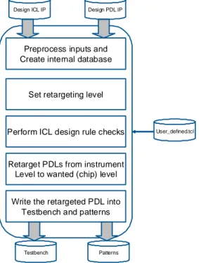
DFT insertion using Tessent IJTAG tool is shown in figure5, where input files are ICL, PDL, and user defined files. The use of such high level languages is very advantageous since it decreases considerably the development time and increase the reusability from 2D to 3D. In fact the EDA tool retargets testbenches and patterns according to the configuration files. In our case, the same PDL file can be used at pre-bond level (2D) and post-bond level (3D) which avoid performing the work two times.
Preprocess inputs and Create internal database
Set retargeting level
Perform ICL design rule checks
Retarget PDLs from instrument Level to wanted (chip) level
Write the retargeted PDL into Testbench and patterns
User_defined.tcl
Design ICL IP Design PDL IP
Testbench Patterns
Figure 5. Tessent IJTAG flow
VI. CONCLUSION AND FUTURE WORK
We have presented in this paper 3 DFT proposals based on the IEEE P1687 test standard and on automatic die-detection. A practical implementation on a 3D circuit in a passive interposer was given. Our proposed 3D DFT architecture enables the test of 3D components at all testing levels: pre, mid and post-bond levels by switching between pads and test TSVs using die-detectors. The IEEE P1687 test standard is supported by Mentor Graphics Tessent IJTAG where high level languages can be used which are ICL and PDL to decrease the development time and increase the reuse of test patterns from 2D to 3D.
The next step is to perform analysis of the proposed 3D test architecture in order to make comparison with JTAG based test architecture in terms of cost and test time.
REFERENCES
[1] WideIO JEDEC standard, see http://www.jedec.org/
[2] E.J. Marinissen and Y. Zorian, "Testing 3D chips containing through-silicon vias", in Proc. ITC, 2009, pp.1-11.
[3] Dean L. Lewis, HsienHsin S. Lee "A Scan Island Based Design Enabling Pre-bond Testability in Die Stacked Microprocessors", ITC 2007
[4] Xiaoxia Wu, Paul Falkenstern, Yuan Xie “Scan Chain Design for Three-dimensional Integrated Circuits (3D ICs)”, ICCD 2007 [5] Li Jiang, Lin Huang and Qiang Xu, “Test Architecture Design and
Optimization for Three-Dimensional SoCs”, DATE’09
[6] E.J Marinissen, J Verbree, M Konijnenburg " A structured and scalable test access architecture for TSV-based 3D stacked ICs", in proceedings of VTS 2010, pp. 269 – 274.
[7] E.J Marinissen, Chun-Chuan Chi, J Verbree, M Konijnenburg “A Standardizable 3D DFT Architecture”, 3D-TEST’10
[8] http://grouper.ieee.org/groups/1687/
[9] Erik Larsson and Farrokh Ghani Zadegan, “Accessing Embedded DFT Instruments with IEEE P1687”, in proceedings of ATS 2012, pp. 71-76 [10] "IEEE Standard Test Access Port and Boundary-Scan Architecture",
IEEE Std 1149.1-2001.
[11] Alfred L. Crouch, “IJTAG: The Path to Organized Instrument Connectivity”, in proceedings of ITC2007
[12] J.Rearick, B.Eklow, K.Posse, A.Crouch, B.Bennetts “IJTAG (Internal JTAG): A Step Toward a DFT Standard” , in proceedings of ITC2005 [13] Y.Fkih, P.Vivet, B.Rouzeyre, M-L.Flottes, G.Dinatale “A JTAG based
3D DFT architecture using automatic die detection”
[14] http://electronicdesign.com/boards/what-s-difference-between-jtag-ieee-11491-and-ijtag-ieee-IEEE P1687
[15] M.Keim, F.Hapke, T.Waayers, R.Morren, “Automated Test Creation For Mixed Signal IP Using IJTAG”, white paper Mentor Graphics
View publication stats View publication stats