HAL Id: hal-01655116
https://hal.archives-ouvertes.fr/hal-01655116
Submitted on 29 Jul 2020
HAL is a multi-disciplinary open access
archive for the deposit and dissemination of sci-entific research documents, whether they are pub-lished or not. The documents may come from teaching and research institutions in France or abroad, or from public or private research centers.
L’archive ouverte pluridisciplinaire HAL, est destinée au dépôt et à la diffusion de documents scientifiques de niveau recherche, publiés ou non, émanant des établissements d’enseignement et de recherche français ou étrangers, des laboratoires publics ou privés.
Suppressing the memory state of floating gate transistors
with repeated femtosecond laser backside irradiations
Maxime Chambonneau, Sarra Souiki-Figuigui, Philippe Chiquet, Vincenzo
Marca, Jérémy Postel-Pellerin, Pierre Canet, Jean-Michel Portal, David Grojo
To cite this version:
Maxime Chambonneau, Sarra Souiki-Figuigui, Philippe Chiquet, Vincenzo Marca, Jérémy Postel-Pellerin, et al.. Suppressing the memory state of floating gate transistors with repeated femtosec-ond laser backside irradiations. Applied Physics Letters, American Institute of Physics, 2017, 110, pp.161112 - 161112. �hal-01655116�
1
Suppressing the memory state of floating gate transistors with
repeated femtosecond laser backside irradiations
Maxime Chambonneau1,a), Sarra Souiki-Figuigui2, Philippe Chiquet2, Vincenzo Della Marca2, Jérémy Postel-Pellerin2, Pierre Canet2, Jean-Michel Portal2, and David Grojo1,b)
1Aix-Marseille University, CNRS, LP3, F-13288 Marseille, France 2Aix-Marseille University, CNRS, IM2NP, F-13397 Marseille, France a)Electronic mail: [email protected]
b)Electronic mail: [email protected]
Abstract
We demonstrate that infrared femtosecond laser pulses with intensity above two-photon ionization threshold of crystalline silicon (c-Si) induce charge transport through the tunnel oxide in floating gate Metal-Oxide-Semiconductor (MOS) transistor devices. With repeated irradiations of Flash memory cells, we show how the laser-produced free-electrons naturally redistribute on both sides of the tunnel oxide until the electric field of the transistor is suppressed. This ability enables to determine in a nondestructive, rapid and contactless way the flat band and the neutral threshold voltages of the tested device. The physical mechanisms including nonlinear ionization, quantum tunneling of free-carriers, and flattening of the band diagram are discussed for interpreting the experiments. The possibility to control the carriers in memory transistors with ultrashort pulses holds promises for fast and remote device analyses (reliability, security, defectivity) and for new developments in the growing field of ultrafast microelectronics.
The interaction between focused infrared femtosecond laser pulses and bulk crystalline silicon (c-Si) results in the formation of microplasmas1 by multiphoton ionization.2, 3 Thereby, one could expect to reach the critical electron density of c-Si by simply increasing the laser intensity. However, a recent theoretical study has demonstrated that this density cannot be reached with femtosecond laser irradiation due to plasma defocusing phenomenon which prevents the material from any permanent modification.4 It is thus natural to investigate the possibility to handle the free-carriers produced in this regime of self-limited excitation. The most likely field where such a study can be applied is microelectronics. In this context, several studies have been conducted during the last decade on laser-transistor interactions.5-7 Although these works have shown an impact of the laser on the device, irradiations at 1064 nm were involved implying only modest free-carrier production (ionization) at the transistor region. To solve this issue, El-Mamouni et al. employed a longer wavelength performing laser experiments relying on localized two-photon ionization on fin field-effect transistors (FinFETs).8 Due to the nonlinear nature of the ionization of c-Si by photons with sub-bandgap energy, the volume of the subsequent plasma is extremely confined with a high electron density. Nevertheless, FinFETs are multigate structures making difficult the evaluation of the laser effect on each gate individually. Among all the existing microelectronic devices, one of the most relevant that is able to store laser-produced free-carriers is the Flash memory due to the possibility to evaluate the number of carriers trapped inside the floating gate (FG) of the device.9-11 This latter is the place where electrons can be stocked, defining the logical state of the memory. When no charge is stored in the FG, the particular value of the threshold voltage (𝑉𝑡) of the Flash cell is called the neutral threshold voltage (𝑉𝑡0). This state used to be reached after ultraviolet (UV) frontside exposure imparting to electrons sufficient energy to migrate inside or outside the floating gate.12 However, this technique is not applicable anymore for advanced technologies because the stacks of metalused for electrical circuitry prevent UV penetration. Since the knowledge of𝑉𝑡0 is crucial for the characterization and the reliability assessment of Flash memories,13 the elaboration of a nondestructive, rapid and contactless experimental method for determining this parameter is essential.
2
In the present Letter, we show that charge carriers can be injected inside or outside the floating gate of Flash memories with repeated femtosecond laser backside irradiations at 1300 nm. An identical final state, characterized by an experimentally measured flat band threshold voltage (𝑉𝑡𝑓𝑏), is reached after multiple irradiations for initially erased and programmed devices. This state is interpreted as the one for which the electric field is removed in the tunnel capacitor of the memory cell thanks to a theoretical scenario consistent with the reported experiments and our previous works. Finally, the neutral threshold voltage can beretrieved
from the flat band threshold voltage.
The investigated microelectronic devices are single isolated Flash floating gate memory cells (90 nm width, 180 nm length) integrated on a 200 mm wafer using a standard NOR Flash process. The silicon FG is isolated from the control gate (CG) with Oxide-Nitride-Oxide [ONO (SiO2/Si3N4/SiO2, 15.7 nm equivalent
oxide thickness)] inter-poly dielectric stack layer, and also separated from the substrate (p-type c-Si) with a
9.6 nm thick tunnel oxide layer (SiO2). The source and the drain are both in n-type c-Si. The experimental set-up specifically designed for irradiating the cells is detailed in Ref. 11. Briefly, it relies on a customized inverted microscope in which a femtosecond laser beam is injected. A titanium-sapphire laser source (Spectra-Physics, Hurricane) produces pulses of 100 fs at 1 kHz repetition rate (i.e., 1 ms between two
consecutive pulses). This rate not only provides timely-fashioned experiments, but also ensures that there is
neither interaction between one pulse and the free-carriers produced in silicon by the preceding one, nor heat
accumulation on a pulse-to-pulse basis, regarding the nanosecond timescale of recombination14 and thermal
effects.15 The beam converted at 1300 nm wavelength (photon energy 0.95 eV) by optical parametric
amplification (Spectra-Physics, 800CF) is then focused inside the silicon wafer from the polished backside surface using an objective lens (Mitutoyo, 50× Plan Apo NIR Infinity Corrected) of numerical aperture 0.42 mounted on a motorized-stage along the optical axis. At the focus, the beam is Gaussian-shaped and the diameter at 1/e2 is around 2 µm. The Rayleigh length in c-Si is around 8.2 µm, which is much larger than the size of the device. The focus is kept constant during the whole irradiation, and the energy is maintained at 440 pJ (maximum intensity ~280 GW/cm2) with fluctuations < 5% peak-to-peak, ensuring high electron density (~1018 cm-3) without strong plasma defocusing.4 The irradiated zone is positioned with the help of a customized microscope based on a light-emitting diode at 1200 nm for illumination and an InGaAs camera (WiDy SWIR 320U) for imaging. In addition to the optical set-up, a probe station is placed on the front side of the wafer for in situ programming, erasing, and also measuring the electrical properties of the irradiated device before and after each laser pulse. It consists in a four-terminal sensing arrangement connected to the control gate, the drain, the source, and the substrate of the Flash memory cell. The four terminals are connected to a precision semiconductor parameter analyzer (Agilent, 4156C), enabling us to evaluate the drain current (𝐼𝐷) as a function of the control gate voltage (𝑉𝐶𝐺) (𝐼𝐷-𝑉𝐶𝐺 curve) that we use to directly estimate the charge of the FG (see hereafter). Prior to laser irradiation, the devices are erased or programmed
in the following classical conditions:10 𝑉
𝐶𝐺 = −18 V, 𝑉𝐷 = 𝑉𝑆 = 𝑉𝐵= 0 V during 1 ms for erasing, and
𝑉𝐶𝐺 = +9 V, 𝑉𝐷 = +4 V, 𝑉𝑆 = 𝑉𝐵 = 0 V during 5 µs for programming, where 𝑉𝐷, 𝑉𝑆 and 𝑉𝐵 are the
voltages of the drain, source and bulk, respectively.
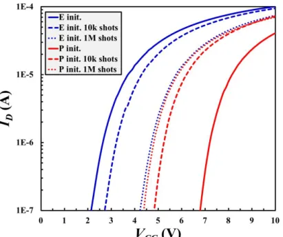
The 𝐼𝐷-𝑉𝐶𝐺 curves of two similar isolated Flash memory cells initially erased and programmed are displayed in Fig. 1 (solid lines). The 𝐼𝐷-𝑉𝐶𝐺 curveof the programmed cell is comparable to the erased one, but shifted of +4.6 V. This is a consequence of the presence of holes or electrons inside the FG in the erased and the programmed configuration, respectively. An identical sequence of laser pulses is then applied on each cell. In the erased configuration, the 𝐼𝐷-𝑉𝐶𝐺 curve is shifted toward the programmed state after irradiation. Conversely, for the initially programmed state, the 𝐼𝐷-𝑉𝐶𝐺 curve is shifted toward the erased state, without a sub-threshold slope degradation.16 These results directly suggest that the repeated laser radiations provoke free-carrier separation, migration, and recombination from or into the FG, and thus a partial programming/erasing operation.
3
Fig. 1. Evolution of the drain current 𝐼𝐷 as a function of the control gate voltage 𝑉𝐶𝐺 for two similar isolated Flash memory cells initially erased (blue) and programmed (red), and for different number of applied pulses.
In order to analyze more precisely the impact of laser radiation on the trapped charge in the Flash memory, the threshold voltage 𝑉𝑡, defined as the CG voltage for which 𝐼𝐷 = 1 µA, can be monitored. It is strongly related to the amount of charges stored inside the FG,10 and can be expressed as
𝑉𝑡 = 𝑉𝑡0 − 𝑄𝐹𝐺⁄𝐶𝑂𝑁𝑂 (1)
where 𝑄𝐹𝐺 is the charge of the FG, and 𝐶𝑂𝑁𝑂 = 1.2 × 10⁻¹⁶ F is the estimated capacitance of the CG/ONO/FG stack. In Fig. 2, 𝑉𝑡 is reported as a function of the number of laser pulses (in logarithmic scale) for the same two cells tested in Fig. 1. Starting from the initial state, 𝑉𝑡 varies very weakly (<4% of its initial value, i.e., in the error bar of the probe station) for a number of shots <1000. However, a significant modification of the threshold voltage is observed between 1000 and 30000 shots. For higher number of shots, 𝑉𝑡 weakly increases, highlighting a saturation of the laser-induced programming and erasing phenomena. One can note that the final 𝑉𝑡 value reached after one million shots is the same (~4.8 V) independently from the initial state of the cell. According to Eq. (1), the increase and the decrease in 𝑉𝑡 in Fig. 2 (in the initially erased and programmed configuration, respectively) suggest a transport of free-carriers toward and from the FG, respectively. The charge difference ∆𝑄𝐹𝐺 between two states can be estimated as
∆𝑄𝐹𝐺 = −𝐶𝑂𝑁𝑂∆𝑉𝑡 (2)
where ∆𝑉𝑡 is the difference in threshold voltage between the two states. Between the final and the initial
state, ∆𝑄𝐹𝐺 is quantitatively estimated to be −2.5 × 10⁻¹ and 2.9 × 10⁻¹ fC for the initially erased and
programmed cell, respectively. In other words, after one million laser shots ~1700 electrons have migrated from or toward the FG in both configurations, as emphasized by the empty symbols in Fig. 2. We attribute the weak differences in the electron transport dynamics between the erased and the programmed cell to the
laser fluctuations and positioning. In a previous study, we have shown that 𝑉𝑡= 4.8 V could be exceeded
employing laser energies higher than 10 nJ.11 Nevertheless, for such energies, the irradiations also provoke irreversible degradations of the drain/bulk and source/bulk junctions, resulting in an alteration of the shape of the 𝐼𝐷-𝑉𝐶𝐺 curves. In the present study with low pulse energy, no degradation of the aforementioned junctions was measured as highlighted by the shifts of the 𝐼𝐷-𝑉𝐶𝐺 curves in Fig. 1 without alteration of the shape.
4
Fig. 2. Evolution of the threshold voltage 𝑉𝑡 (full symbols) and the cumulative number of transported electrons (empty symbols) according to Eq. (2) as a function of the number of laser pulses for the same two cells tested in Fig. 1.
Several physical mechanisms can be advanced for explaining the experimental results shown in Figs. 1 and 2. We propose a theoretical scenario including four main steps occurring chronologically in Fig. 3 for initially erased and programmed cells irradiated by one single laser pulse. The first step consists in laser pulse delivery to the cell region during ~100 fs. Comparing the width and length of the Flash memory (~100 nm) with the beam diameter and Rayleigh length (~10 µm), the laser intensity can be considered as uniform through the cell. The second mechanism is two-photon ionization of the silicon parts of the Flash memory. Regarding the pulse duration, this process is instantaneous and leads to the formation of a plasma (electrons in red in Fig. 3) with an electron density independent on the initial state of the cell.2 According to Ref. 4, even in the cases where the pulse energy is increased, the electron density should be around 1018 cm -3, and cannot be significantly increased due plasma defocusing. It is worth noting that, since the bandgap of silica is around 9 eV, ten photons at 1300 nm are necessary to ionize the tunnel oxide, and the associated intensity threshold for ionization is 2 × 10⁴ GW/cm2,3 well above the intensity in our experiments. Thereby, the oxide layer is considered as unaffected by the laser radiation.
Then, several free-carriers are able to tunnel through the oxide layer (third mechanism). In Figs. 3(a) and (b), only the electrons are represented for tunneling, and the contribution of the holes is neglected. This assumption is reasonable since for low particle energy (< 1.12 eV), the probability for holes to tunnel is calculated to be at least 17 decades lower than the one for electrons using the Wentzel–Kramers–Brillouin approximation. The direction of the electron migration (from the FG toward the substrate, or inversely) depends on the initial configuration of the cell. Indeed, when the cell is initially erased, the FG mainly contains holes and its potential is positive. Hence, the electric field in the tunnel oxide (on which the
tunneling probability is strongly dependent) is also positive, and the energetic laser-produced free-electrons
in the substrate are attracted toward the FG. Conversely, when the cell is initially programmed, the FG mainly contains electrons and its potential as well as the electric field in the tunnel oxide are negative. In this case, the laser-produced free-electrons are thus injected into the substrate. In order to illustrate this mechanism in the two configurations, we have calculated in Figs. 3(a) and (b) the initial band diagrams (solid black lines) and the ones after the FG has lost 50% of its initial charge (dotted blue lines) by solving Poisson’s equation along the Si/SiO2/Si structure, and assuming the tunnel oxide is not degraded during laser irradiation (i.e., its net electrical charge remains negligible).
One could also consider electron transport over the oxide energy barrier (i.e., thermionic emission) rather than quantum tunneling.17 Nevertheless, as indicated by the band diagrams in Fig. 3, the energy difference
5
between the bottom of the conduction bands of c-Si and SiO2 is 3.1 eV. This difference is too important for considering thermionic emission because the absorption of the laser flux by free-electrons in c-Si is quenched by avalanche ionization. This is suggested by the flux-doubling model,18 which implies that the energy of the free-electrons generated by ultrashort pulses is essentially under 1.12 eV, corresponding to the bandgap of silicon.
Finally, the electrons recombine with holes in a few nanoseconds after the pulse,14 and the electron separation, migration, and recombination result in a partial flattening of the band diagram in both initial situations (fourth mechanism). By repeating pulse-to-pulse this scenario, the shrinkage of the oxide potential becomes more and more pronounced (i.e., the electric field in the tunnel oxide tends to zero), and the band diagram is increasingly flat. Once the band diagram is completely flat (Fig. 3(c)), the probability for electrons to tunnel is identical in both directions so that, on the average, there is no electron exchange between both electrodes. This is consistent with the stabilization experimentally observed in Fig. 2. In this final configuration, the electric field in the tunnel oxide and the electrodes has been neutralized, and the 𝑉𝑡 value that can be measured is 𝑉𝑡𝑓𝑏. As experimentally emphasized in Figs. 1 and 2, this final value is
independent of the initial state of the Flash memory. However, the initial conditions [i.e., erased (𝑉𝑡 ≈
2.6 V) or programmed (𝑉𝑡 ≈ 7.2 V)] mainly influence the orientation and the value of the electric field, as
well as the initial tunnel oxide voltage (calculated to be +0.97 V and −1.22 V for initially erased and
programmed cells, respectively). In our previous study, we have performed similar experiments on initially
erased cells applying a voltage on the CG during the laser pulses.11 The evolution of 𝑉𝑡 as a function of the number of pulses was found to be accelerated for 𝑉𝐶𝐺 = +3 V, and decelerated for 𝑉𝐶𝐺 = −3 V, by comparison with the configuration where no CG bias is applied. These results are strongly consistent with the proposed scenario of Fig. 3 since applying a bias modifies the initial band diagram, and thus the probability for electrons to tunnel.
Finally, as shown in the Supplementary Material section, 𝑉𝑡0 can be retrieved from 𝑉𝑡𝑓𝑏 as
𝑉𝑡𝑓𝑏 = 𝑉𝑡0 − 𝑉𝑓𝑏⁄ 𝐾 (3)
where 𝑉𝑓𝑏 is the flat band voltage of the tunnel capacitor (FG/tunnel oxide/substrate), and 𝐾 is a factor accounting for the geometry of the device. The difference in value between 𝑉𝑡0 and 𝑉𝑡𝑓𝑏 is due to the presence of electrons in the FG in the flat band configuration as depicted in Fig. 3(c). Using 𝑉𝑡𝑓𝑏 = 4.8 V according to Fig. 2, 𝑉𝑓𝑏 = −1.04 V as calculated at ambient temperature and 𝐾 ≈ 0.7, 𝑉𝑡0 is found to be
close to 3.3 V. This shows that it is possible to determine the neutral threshold voltage of a Flash memory by repeated infrared femtosecond laser backside irradiations.
6
Fig. 3. Physical mechanisms occurring during femtosecond irradiation of a Flash memory initially (a) erased and (b) programmed. The top images correspond to a schematic description of the interaction. The bottom images result from a calculation of the initial band diagram of the tunnel capacitor, and the one after the floating gate has lost 50% of its initial charge. The top and bottom curves correspond to the bottom of the conduction band and the top of the valence band respectively. The flat band configuration (c) results from repeated irradiations described in (a) and (b).
In summary, we have established that repeated femtosecond laser irradiations at 1300 nm are able to induce a transport of electrons across the tunnel oxide of Flash memories. The electrical state resulting of one million pulses is independent on the initial one. A theoretical scenario has been proposed for interpreting this final state as the one for which the band diagram of the tunnel capacitor is flat. Moreover, the measurement of this state enables the evaluation of the neutral threshold voltage for which no charge is in floating gate. This study not only provides an experimental method for determining paramount parameters of transistors, but also paves the way to rapid and contactless reliability tests of Flash memories for smart applications.
Acknowledgements
This work has been carried out thanks to the support of the A*MIDEX project (n°ANR-11-IDEX-0001-02) funded by the “Investissements d’Avenir”, French Government program, managed by the French National Research Agency (ANR).
References
1A. Mouskeftaras, A. V. Rode, R. Clady, M. Sentis, O. Utéza, and D. Grojo, Appl. Phys. Lett. 105, 191103 (2014). 2S. Leyder, D. Grojo, P. Delaporte, W. Marine, M. Sentis, and O. Utéza, Appl. Surf. Sci. 278, 13-18 (2013). 3D. Grojo, S. Leyder, P. Delaporte, W. Marine, M. Sentis, and O. Utéza, Phys. Rev. B 88, 195135 (2013). 4E. V. Zavedeev, V. V. Kononenko, and V. I. Konov, Laser Phys. 26, 016101, (2015).
5S. Skorobogatov, Hardware-Oriented Security and Trust, 2009. HOST'09. IEEE International Workshop on, pp. 1-6 (2009). 6A. Sarafianos, R. Llido, J.M. Dutertre, O. Gagliano, V. Serradeil, M. Lisart, V. Goubier, A. Tria, V. Pouget, and D. Lewis, Microelectronics Reliability 52, 2035-2038 (2012).
7R. Llido, P. Masson, A. Regnier, V. Goubier, G. Haller, V. Pouget, and D. Lewis, Microelectronics Reliability 52, 1816-1821 (2012).
8F. El-Mamouni, E. X. Zhang, N. D. Pate, N. Hooten, R. D. Schrimpf, R. A. Reed, K. F. Galloway, D. McMorrow, J. Warner, E. Simoen, C. Claeys, A. Griffoni, D. Linten, and G. Vizkelethy, IEEE Trans. Nucl. Sci. 58, 2563-2569 (2011).
9C.-Y. Wu, and C.-F. Chen, Solid-State Electronics, 35, 705-716 (1992). 10P. Pavan, R. Bez, P. Olivo, and E. Zanoni, Proc. IEEE, 85, 1248-1271 (1997).
11V. Della Marca, M. Chambonneau, S. Souiki-Figuigui, J. Postel-Pellerin, P. Canet, P. Chiquet, E. Kussener, F. Yengui, R. Wacquez, D. Grojo, J.-M. Portal, and M. Lisart, Reliability Physics Symposium (IRPS), 2016 IEEE International, 7B-4-1, 7B-4-7 (2016).
12R. D. Katznelson, and D. Frohman-Bentchkowsky, IEEE Trans. Electron Dev. 27(9), 1744-1752 (1980).
13G. Tao, H. Chauveau, D. Boter, D. Dormans, and R. Verhaar, Integrated Reliability Workshop Final Report, 2007. IRW 2007. IEEE International, 52-56, (2007).
14A. Mouskeftaras, M. Chanal, M. Chambonneau, R. Clady, O. Utéza, and D. Grojo, Appl. Phys. Lett. 108, 041107 (2016). 15S. K. Sundaram, and E. Mazur, Nature Mater. 1, 217-224 (2002).
16Y.-B. Park, and D. K. Schroder, IEEE Trans. Electron Dev. 45(6), 1361-1368 (1998). 17F. Guthrie, Proc. R. Soc. Lond. 21, 168-169 (1872).