HAL Id: hal-02381831
https://hal.archives-ouvertes.fr/hal-02381831
Submitted on 13 Jan 2020
HAL is a multi-disciplinary open access
archive for the deposit and dissemination of
sci-entific research documents, whether they are
pub-lished or not. The documents may come from
teaching and research institutions in France or
abroad, or from public or private research centers.
L’archive ouverte pluridisciplinaire HAL, est
destinée au dépôt et à la diffusion de documents
scientifiques de niveau recherche, publiés ou non,
émanant des établissements d’enseignement et de
recherche français ou étrangers, des laboratoires
publics ou privés.
for Probing Size-Dependent Single-Nanoparticle
Electrochemistry
Jean-François Lemineur, Jean-Marc Noël, Dominique Ausserré, Catherine
Combellas, Frédéric Kanoufi
To cite this version:
Jean-François Lemineur, Jean-Marc Noël, Dominique Ausserré, Catherine Combellas, Frédéric
Kanoufi. Combining Electrodeposition and Optical Microscopy for Probing Size-Dependent
Single-Nanoparticle Electrochemistry. Angewandte Chemie International Edition, Wiley-VCH Verlag, 2018,
57 (37), pp.11998-12002. �10.1002/anie.201807003�. �hal-02381831�
size-dependent single nanoparticle electrochemistry
Jean-François Lemineur,
[a]Jean-Marc Noël,
[a]Dominique Ausserré,
[b]Catherine Combellas,
[a]Frédéric
Kanoufi*
[a]Abstract: Electrodeposition of nanoparticles, NPs, is a promising
route for the preparation of highly electroactive nanostructured electrodes. By taking advantage of progressive electrodeposition, disordered arrays of wide size distribution Ag NPs are produced. Assorted with surface reaction monitored by the highly sensitive backside absorbing layer optical microscopy (BALM), such array offers a platform for screening size-dependent electrochemistry at the single NP level. Particularly, it allows rationalizing the electrodeposition dynamics at the single >10nm NP, up to the point of quantifying the presence of metal nanoclusters (<2nm), and probing easier NP oxidation with size decrease, either through electrochemical or galvanic reaction.
Nanostructured electrodes are attracting increasing interest in the current energy challenges through the electrocatalysis of chemical reactions. In addition to properties depending on their bulk or surface chemical composition, the activity of NPs relies on their shape, size and also on inter-NP separation distances that control catalysis efficiency and product distribution.1 To
reach the ideal sustainable and electrocatalytic electrode, a rational dispersion of efficient nanocatalysts onto poorly active support is needed. It can be provided through electrodeposition2 which has several advantages as control over nanoscale composition, structure diversity, and good electrical connection. We suggest that electrodeposition, assorted with appropriate in
operando monitoring, can also inspect structure-related effects
in NP electrochemistry. Taking advantage of progressive electrodeposition,2b arrays of wide size distribution of NPs were
produced, which, engaged into further (electro)chemical reactions, will decipher size-related phenomena. This requires monitoring in situ and in real time the deposition process and the individual behavior of many structurally different NPs. It is afforded by optical microscopies through wide field (>50µm2),
high throughput, and nanoscale resolution imaging. They also carry quantitative information over NP structure (size, composition) or to their electrochemical, EC, activity such as double layer charging, catalysis and dissolution kinetics.3 We propose to use a recently described nanoscale optical microscopy technique, BALM (backside absorbing layer microscopy),4 to quantify in situ EC processes related to the case study of Ag NPs. It is first used to explore their electrodeposition. Indeed, several in situ explorations at the single NP level5 have challenged the existing models relying on
EC transients;6 they advocate for the continuous generation of
nanoclusters (NCs, size <2nm). These NCs are important building blocks of larger (>10nm) NPs,6,7 through diffusion and
then aggregation at nuclei sites. These NCs were imaged in situ by TEM,5c or scanning probe microscopies,5a,d while their generation and transport were dynamically monitored from EC transient in a nano-EC-cell confined to few nucleation sites,5e or in extremely diluted solutions.7
We propose to address by BALM the real-time (operando) wide-field imaging of the electrodeposition process, at the single NP level over a wide distribution of sizes, up to the point of probing the presence of NCs. Then, the arrays of electrodeposited Ag NPs are used to inspect size-related phenomena in their oxidation engaged either electrochemically or by electrochemical Ostwald ripening.
First the sensitivity of BALM is appreciated in reference to earlier dark-field or SPR opto-electrochemical studies which inspected for Ag NPs, larger than 30nm, either their i) electrodeposition,3c
ii) dissolution3d,e or iii) galvanic transformation into Au NPs.3f To
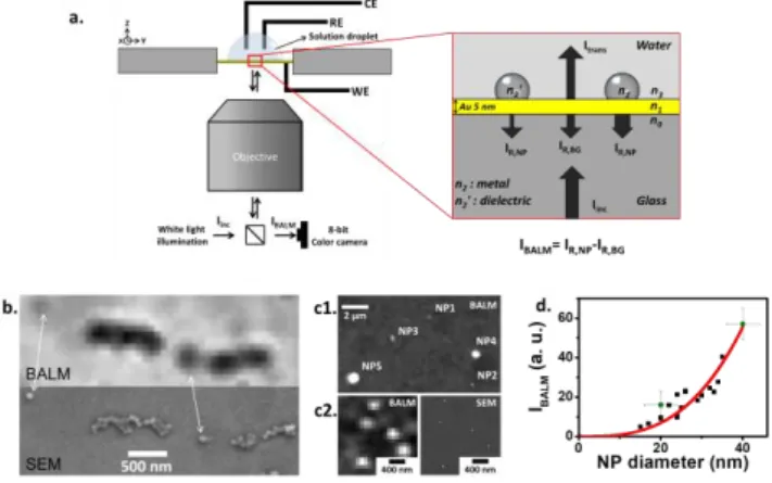
detect smaller NPs, without recourse to deleterious power, a strategy consists in imaging through antireflective substrates.4,8 For a metal, pseudo-antireflective conditions are met when it is deposited as an ultrathin layer (5nm for Au) on glass.4 When illuminated from the backside by an inverted microscope (Figure 1a), such BALM substrate reflects less than 1% of the incident light toward a CCD camera. As SPR or other related reflectance-based methods,9sensitive to local refractive index (n) variations,
BALM images a wide range of materials, from dielectric (Figure 1b) to metal colloids (Figure 1c).
Figure 1. a) Principle of BALM imaging in water based on light reflectance
contrasts; IBALM is estimated from the difference at each pixel of the reflected
light intensity, IR, compared to that reflected by the substrate in the absence of
NP, IR,BG . BALM and SEM images in the same location of b) 90nm polystyrene,
c1) 20 to 100nm Ag, colloids adsorbed or c2) Ag NPs electrodeposited on a BALM substrate and detected as b) negative or c) positive contrasts. d) Sizing of (green, with error bars related to IBALM and size dispersion, averaged over
>10 NPs) adsorbed and (black) electrodeposited Ag NPs comparing IBALM and
the NP size estimated from SEM; red line from Equation (1).
To a first approximation, the BALM intensity, IBALM, was
rationalized from the predicted reflectance (Fresnel equations
[a] J.-F. Lemineur, J.-M. Noël, C. Combellas, F. Kanoufi
Université Sorbonne Paris Cité, Université Paris Diderot, ITODYS, CNRS UMR 7086, 15 rue J. de Baïf, F-75013 Paris, France E-mail: [email protected]
[b] D. Ausserré
Maine University, Institut des Matériaux et Molécules du Mans, CNRS UMR 6283, Avenue O. Messiaen, F-72000 Le Mans, France Supporting information for this article is given via a link at the end of the document.
detailed in the Supporting Information, section S1) of 2 layers (Au thin layer and the probed material) sandwiched between a glass slide and an ambient (water) medium. This predicts, as observed in Figures 1b,c, that metal NPs are detected as bright regions compared to the substrate (increase reflectance), and conversely, dielectric NPs as darker regions (decrease reflectance). As in other optical methods relying on reflectance change,8,9 BALM senses the local change in optical thickness or optical mass (local change in the refractive index and thickness or mass). For deposited thickness values that are small compared to the wavelength, the reflectance change is generally proportional to the amount of deposited material. This lays the foundations for quantitative sizing (mass balance) during the single-NP (electro)chemical transformation.
Experimentally, the sizing performance was evaluated from images of Ag NPs, either adsorbed colloids, or electrodeposited (Figure 1d) on the Au layer. Each kind of NP is definitely differentiated in intensity, the larger the NP the brighter it is (higher IBALM). For both experiments, the background-subtracted IBALM, for individual NPs varies linearly with the NP volume (VNP)
or as the cube of its diameter, dNP, as in other reflectance-based
methods:8,9
𝐼𝐵𝐴𝐿𝑀 = 𝛼𝑉𝑁𝑃= 𝛼𝜋
6(𝑑𝑁𝑃)
3 (1)
The correlation factor, = 1.7x10⁻³ nm-3 from Figure 1d, depends on the Au thickness and optical noise. A reliable NP sizing requires either ex situ SEM or the pre-adsorption of a few colloidal Ag NP as internal size standards for calibration. Even with a standard 8-bit camera, NPs as small as 10±1.5nm (Figure S2a, Supporting Information) were detected at the Au-water interface, making BALM over 30-fold more sensitive (in VNP)
than previous opto-electrochemical reports. The IBALM–volume
(or mass) proportionality is confirmed by the reflectance model, which yields sensitivity estimates for other NPs, 15 nm for Pt or Au and 30nm for polymer.
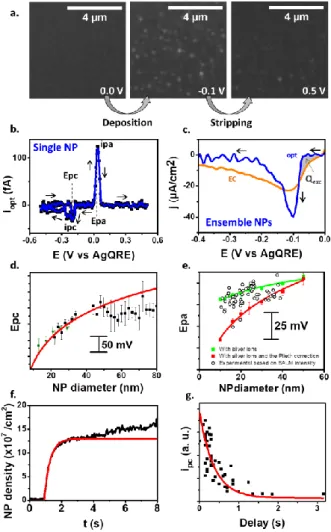
The electrodeposition and the stripping of Ag NPs at a BALM substrate were performed by sweeping its potential (E) along a cyclic voltammetry (CV) in a 100µM AgNO3 and 0.1M NaNO3
aqueous solution (no chloride contamination is expected, see section S1.2, Supporting Information).10 These processes are imaged at an acquisition rate of 20 Hz, to dynamically size, count, and localize NPs (Figure 2a). The electrodeposition produced Ag NPs with sizes from 10 to 80nm, analyzed on a same image and acquisition conditions (see section S2.2, Supporting Information). Individual NP growth/stripping dynamics are inferred from the variation of IBALM with time. From
the IBALM-size relationship [Equation (1)] and Faraday’s law, an
equivalent current, iopt (optical voltammogram, opCV) associated
with the growth (resp. stripping) of individual NPs is inferred: 𝑖𝑜𝑝𝑡 = − 𝐹 𝑉𝑚 𝑑𝑉𝑁𝑃 𝑑𝑡 = − 𝐹 𝛼𝑉𝑚 𝑑𝐼𝐵𝐴𝐿𝑀 𝑑𝑡 (2)
where Vm =10.27 cm3mol-1 is the molar volume of Ag and F the
Faraday constant. Figure 2b (and section S3, Supporting Information) shows the opCV of the electrodeposition of a 21±2nm NP on the cathodic scan, and its stripping on the reverse anodic scan. Each cathodic or anodic process is characterized by a peak potential, Epc and Epa, respectively. The
BALM sizing ability allows relating these Eps to the size of the
electrodeposited NPs (Figure 2d,e). Both Epc and Epa reveal a
shift to more cathodic values when dNP decreases, with a larger
shift for the electrodeposition than for the stripping, suggesting different physical origins.
Apprehending the electrodeposition dynamics allows the control of the NP size distribution. Even if nucleation is often a potential-dependent phenomenon, which leads to more complex nucleation laws,11 the evolution of the surface density of NPs,
N(t), along the cathodic scan of the CV (Figure 2f) can be
rationalized by a potential-independent progressive nucleation law [Equation (3)]:
𝑁(𝑡) = 𝑁0(1 − 𝑒−𝐴×(𝑡−𝑡0)) (3)
where N0 is the NP saturation density, A an apparent
potential-independent nucleation rate constant, and t0 the induction time
(or E) of the deposition. The good fit of the experimental N(t) value by Equation (3) for 3s (equivalently 0.3V larger than the 0.15V range of Epc variations) suggests that the nucleation
process can be analyzed by time or potential-independent N0
and A values.
Figure 2. Monitoring the CV electrodeposition/stripping of Ag NPs (scan rate,
v=0.1V/s). From a) BALM images, the variation of IBALM of a bright spot (NP) is
converted into b) single NP opCV (b), from which Epc and Epa size-dependency
is inferred ((d) and (e), respectively). c) Comparison of background subtracted EC (orange) and ensemble optical (blue) current densities for Ag+ reduction; the shaded area reveals the EC contribution of NCs (invisible in BALM). d,e) Ep variations with NP size, from opCVs (symbols, two independent experiments in (d), 350 NPs, binned by 3nm) compared to (d) Equation 6 or
(e) COMSOL simulations (lines). f) NPs count over a 10x10µm area during CV yields nucleation dynamics Equation (3) with N0 = 1.3x10⁸ NP cm-2 and A =
2.7 s-1 (red = fit to equation); g) Evolution of individual NP peak currents with its birth time is fitted by Equation 5 (red line) with the same A value.
Figures 2d,g show that these expressions are satisfied experimentally with the same value of A extracted from the NP count (Figure 2f), showing the full consistency of the analysis. Particularly, Equation (6) explains the observed cathodic shift of
Epc with NP size during electrodeposition. Indeed, the Epc values
reflect each NP birth time: the later a NP nucleates, the smaller it ends up. Unlike stated in previous report,3c the main contribution of the Epc-size variations cannot be accounted for
size-dependent thermodynamics (see below) but to the probability of nucleation. Equation 6 also allows controlling or inferring NP size-distribution from the nucleation rate, which can be tuned, for example, by diluting the Ag+ precursor ions or examining the early stage of the nucleation.
In this early stage, NCs are generated that later aggregate into larger NPs. NCs cannot be resolved but are indirectly probed by BALM. Figure 2c compares the optical current density (blue) accumulated over 100 NPs, and the background-subtracted EC current density (orange) recorded by the potentiostat. The optical trace is delayed by 0.07V (0.7s), but decreases faster and reaches a more negative peak value compared to the EC one. These discrepancies suggest a charge mismatch at the early stage of the electrodeposition, attributed5 to the NCs generation. The EC current probes the NCs electrogeneration while the opCV probes their later aggregation into NPs. The NCs density at the onset of the opCV was estimated from the EC charge density exchanged till this onset, represented by the shaded area in Figure 2c. Assuming the generation of a 2nm NC requires QNC=0.04 fC, the excess charge density Qexc=
3.6µC/cm2 yields a NC density at the onset of the opCV of N0,NC
= 9x1010 cm-2, in good agreement with reported values.5c The NCs diffusion-aggregation should be deduced by comparing the EC and optical currents as they describe resp. the flux of NC generation and of their diffusion-aggregation into NPs, respectively, however this remains speculative owing to the small fraction of electrode optically monitored.
Once electrogenerated, the oxidation of individual NPs was also studied by BALM. When the NPs size decreases, their free energy is expected to increase as a result of an increase of surface curvature. Plieth12 proposed that the standard potential of NPs, E0NP, varies with dNP [Equation (7)]:
𝐸𝑁𝑃0 = 𝐸𝑏𝑘0 −4𝑉𝐹𝑑𝑚𝑁𝑃𝛾 (7)
where is the surface tension of the material, and tends toward the bulk material value, E0bk, for large NPs. For bulk Ag,13Ag
1.5Jm-2 while Zamborini reported higher values from ensemble EC data.13b This shows the difficulty in properly elucidating
size-dependent thermodynamics. Indeed, rather than 𝐸𝑁𝑃0 , one measures a peak potential, Epa, representing the behavior of the
ensemble NPs. But Epa strongly depends on the NP surface
coverage,13,14 or on possible contamination (i.e. Cl– in the sub µM range affects the Ag Epa). The rationalization of the
electrodeposition process, presented earlier, allows generating an array of Ag NPs with a wide size distribution. Monitoring the array oxidation by BALM ensures that Epa for the distribution of
NPs is evaluated individually and all at once within the same experimental conditions. The local surface occupied by each NP is also monitored and accounted for, spanning from 0.3 to 1.4 µm2 during the stripping. The stripping within the range of NP
surface coverage and sizes was simulated by COMSOL (green line in Figure 2e), showing that in the absence of Plieth correction (7), Epa remains constant within 5-10mV. Particularly,
performing the stripping in the presence of 100µM Ag+, acting as a buffer of concentration polarization, reduces (Figure S4, Supporting Information) the surface coverage impact on Epa and
the apparent decrease of Epa with NP size. These effects may
have been underestimated in earlier works explaining overestimation of the size-effect.13b Considering the Plieth
correction, the simulation (red line) predicts a negative shift of Epa by 40mV when the NP decreases from 50 to 12nm.
Experimentally (Figure 2e), the Epa variations suggest a Ag value
smaller than and consistent with that of bulk Ag. It confirms a recent EC reexamination13a and highlights that size-effect in E0NP
is critical to estimate for NPs larger than 10nm.
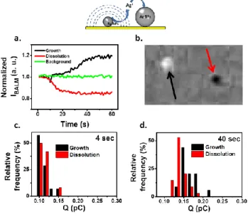
Finally, the sensitivity of the BALM is used to monitor the consequence of Plieth correction in a chemical environment (no polarization). Indeed, Equation (7) suggests that conductive substrates structured with Ag NPs of different sizes are unstable. Even in the absence of external polarization, when electrically contacted, a small and neighboring large NP create a Galvani corrosion cell: the large NP growing at the expense of the small one. Such a situation, known as the electrochemical Ostwald ripening, is monitored in Figure 3 but cannot be quantified from direct EC measurement as no overall current is exchanged with the exterior. Optical microscopies are able to detail its dynamic, as reported for Galvanic replacement3f or bipolar electrochemical systems.15
Figure 3. a) Example of normalized IBALM variations of two Ag NPs over time in
ultra-pure water (open circuit). b) Difference (3.1µm wide) between two optical images recorded at 1min interval in a region where a NP dissolves (red arrow) and another grows. Charge distribution for dissolution/growth of individual NPs, calculated from BALM images, for c) 4 and d) 40s.
An array of electrodeposited Ag NPs of various sizes was washed and exposed to ultra-pure water, while being monitored by BALM. The IBALM transients at various locations (NPs or
background) were analyzed: normalized from the IBALM values at
the same location on the first image they reflect local Ag material deposition/dissolution. Figure 3a presents the size variations of two NPs separated by less than 2µm while Figure 3b highlights them by the opposite contrasts in a difference image. Obviously, one NP grows while the other dissolves, a behavior confirmed for more than 30 NPs. Based on Equation (2), the charge transferred from each single NP growth or dissolution is estimated (for t=4 and 40s see Figures 3c and 3d, resp. and Figure S5a, Supporting Information). At its earliest stages, the partial or complete dissolution corresponds to 0.1pC (14nm NP). Meanwhile, a similar cathodic charge is detected for the NP growth suggesting the full conversion of the process and therefore a concerted mechanism. A deeper mechanistic analysis of Ag+ dilution is intricate (COMSOL simulation in section S5.2, Supporting Information) as it depends on the contributions of all neighboring NPs. Such a simulation however explains that (Figure 3a) the onset of the neighbor NP growth is concomitant, but with slower rate, to the NP dissolution. The surface reconstruction process is slow: the charges exchanged increase with time, but still with overall charge balance in agreement with a corrosion mechanism.
In conclusion BALM, which is an ultra-sensitive optical microscopy relying on local reflectance changes at an absorbing material (here Au), was used to image and size dynamically and
in situ dielectric and metallic NPs. We show how BALM images
can quantify the local electrodeposition or stripping of Ag nanomaterial onto a BALM electrode to the point of producing single NP voltammograms associated to these processes down to 10nm NP. The controlled electrodeposition process produces arrays of Ag NPs of wide size distribution. Such platform, through BALM monitoring, provides new insight into nanoscale electrochemistry. Comparing the electrochemical and optical response indirectly supports the contribution of nanoclusters aggregation during 3D NP electrodeposition. Then the NP arrays were used to analyze in the same experiments size-dependent electrochemistry at the single NP level. We show that size effect has different origins: the NP nucleation probability for the electrodeposition potential and a surface energy contribution for the electrodissolution potential. In the latter case, we confirm, at the single NP level, recent reports showing that surface energy contributions are often overestimated. Finally, the method was extended to more general chemical NP transformation exemplified here in the in situ visualization and quantification of electrochemical Ostwald ripening.
Acknowledgements
We are grateful for financial support by the Agence Nationale pour la Recherche (NEOCASTIP-ANR-15-CE09-0015-02).
Keywords: electrodeposition • optical microscopy • single
nanoparticle electrochemistry • size effects
References
[1] C. Costentin, C. di Giovanni, M. Giraud, J.M. Savéant, C. Tard, C. Nat. Mat. 2017, 16, 1016-1022.
[2] a) S.E.F. Klein, S.C.S. Lai, T.M. Koper, P.R. Unwin, Angew. Chem. Int. Ed. 2014, 53, 3558-3586; b) R.M. Penner, J. Phys. Chem. B 2002, 106, 3339-3353.
[3] a) W. Wang, Chem. Soc. Rev. 2018, 47, 2485-2508; b) Y. Wang, X. Shan, N.; Tao, Faraday Discuss. 2016, 193, 9-39; c) C.M. Hill, S. Pan, J. Am. Chem. Soc. 2013, 135, 17250-17253; d) Y. Fang, W. Wang, X. Wo, Y. Luo, S. Yin, Y. Wang, X. Shan, N. Tao, N. J. Am. Chem. Soc.
2014, 136, 12584–12587; e) V. Brasiliense, A.N. Patel, A. Martinez-Marrades, J. Shi, Y. Chen, C. Combellas, G. Tessier, F. Kanoufi, J. Am. Chem. Soc. 2016, 138, 3478–3483; f) J. Smith, Q. Yang, P.K. Jain, Angew. Chem. Int. Ed. 2014, 53, 2967–2872.
[4] a) S. Campidelli, R.A. Khachfe, K. Jaouen, J. Monteiller, C. Amra, M. Zerrad, R. Cornut, V. Derycke, D. Ausserré, Sci. Adv. 2017, 3, e1601724; b) http://www.watchlive.fr/index.php/en/ Accessed June 13, 2018.
[5] a) J.V. Zoval, R.M. Stiger, P.R. Biernacki, R.M. Penner, J. Phys. Chem.
1996, 100, 837-844; b) A. Radisic, P.M. Vereecken, J. B. Hannon, P.C.
Searson, F.M. Ross, NanoLett. 2006, 6, 238-242; c) J. Ustarroz, J.A. Hammons, T. Atlantzis, A. Hubin, S. Bals, H. Terryn, J. Am. Chem. Soc.
2013, 135, 11550-11561; d) R L. Harniman, D. Plana, G.H. Carter, K.A.
Bradley, M.J. Miles, D.J. Fermin, Nat. Comm. 2017, 8, 971; e) S.C.S. Lai, R.A. Lazenby, P.M. Kirkman, P.R. Unwin, Chem. Sci. 2015, 6, 1126-1138.
[6] M.E. Hyde, R.G. Compton, J. Electroanal. Chem. 2003, 549, 1-12. [7] J. Kim, J.E. Dick, A.J. Bard, Acc. Chem. Res. 2016, 49, 2587-2595. [8] G.G. Daaboul, A. Yurt, X. Zhang, G.M. Hwang, B.B. Goldberg, M.S.
Ünlü, NanoLett. 2010, 10, 4727–4731.
[9] a) S. Wang, X. Shan, U. Patel, X. Huang, J. Lu, J. Li, N. Tao, Proc. Nat. Acad. Sci. 2010, 107, 16028-16032; b) S. Munteanu, J. P. Roger, Y. Fedala, F. Amiot, C. Combellas, G. Tessier, F. Kanoufi, Faraday Discuss. 2013, 164, 241-258; c) S. Munteanu, N. Garraud, J. P. Roger, F. Amiot, J. Shi, Y. Chen, C. Combellas, F. Kanoufi, Anal. Chem. 2013, 85, 1965-1971.
[10] K. Ngamchuea, R.O.D. Clark, S. V. Sokolov, N.P. Young, C. Batchelor-McAuley, R.G. Compton, Chem. A Eur. J. 2017, 23, 16085-16096. [11] A. Milchev, J. Electroanal. Chem. 1998, 457, 35-46.
[12] W.J. Plieth, J. Phys. Chem. 1982, 86, 3166–3170.
[13] a) C.C. M. Neumann, C. Batchelor-McAuley, K. Tschulik, H.S. Toh, P. Shumbula, J. Pillay, R. Tshikhudo, R.G. Compton, ChemElectroChem
2014, 1, 87-89; b) O.S. Ivanova, F.P. Zamborini, J. Am. Chem. Soc. 2010, 132, 70-72.
[14] H.S. Toh, C. Batchelor-McAuley, K. Tschulik, M. Uhlemann, A. Crossley, R.G. Compton, Nanoscale 2013, 5, 4884–4893.
[15] M. Hasheminejad, Y. Fang, M. Li, Y. Jiang, W. Wang, H.Y. Chen, Angew. Chem., Int. Ed. 2017, 56, 1629-1633.
Layout 1:
COMMUNICATION
Disordered arrays of wide size distribution of Ag nanoparticles are
generated by progressive
electrodeposition. Combined to highly sensitive optical microscopy such platform grants access to size-dependent single nanoparticle electrochemistry.
J.-F. Lemineur, J.-M. Noël, D. Ausserré, C. Combellas, F. Kanoufi*
Page No. – Page No.
Combining electrodeposition and optical microscopy for probing size-dependent single nanoparticle electrochemistry