ANALOG ADAPTIVE NONLINEAR FILTERING AND SPECTRAL
ANALYSIS FOR LOW-POWER AUDIO APPLICATIONS
by
Christopher D. Salthouse
S.B.
Electrical Engineering
Massachusetts Institute of Technology, 2000
M.Eng Electrical Engineering
Massachusetts Institute of Technology, 2000
SUBMITTED TO THE DEPARTMENT OF ELECTRICAL ENGINEERING IN
PARTIAL FULFILLMENT OF THE REQUIREMENTS FOR THE DEGREE OF
DOCTOR OF PHILOSOPHY IN ELECTRICAL ENGINEERING AT THE
MASSAHCUSETTS
INSTITUTE
OF TECHNOLOGY
AUGUST 2006
Signature of the Author:
MASSACHUSE'TS WIN KITE• OF TECHNOLOGY
JAN 1.1
2007
.LIBRARIES
Department of Electrical Engineering
August
8th,2006
AftCRCI
Certified by:
Rahul Sarpeshkar
ociate
Profe.sor of
lectrical Engineering
-
hsis
Supervisor
S-- .r
Accepted by:
Arthur C. Smith
Chairman, Department Committee on Graduate These
© 2006 Massachusetts Institute of Technology. All rights reserved.
-ANALOG ADAPTIVE NONLINEAR FILTERING AND SPECTRAL
ANALYSIS FOR LOW-POWER AUDIO APPLICATIONS
by
Christopher D. Salthouse
Submitted to the Department of Electrical Engineering and Computer Science on August 8", 2006 in Partial Fulfillment of the Requirements for the
Degree of Doctor of Philosophy in Electrical Engineering
Abstract
Filters are one of the basic building blocks of analog circuits. For linear operation, the power consumption is proportional to the dynamic range for a given topology. I have explored techniques to lower the power consumption below this limit by extending operation beyond the linear range.
First, I built a power-efficient linear gm-C filter that demonstrates that dynamic range can be shifted to higher linear ranges using capacitive attenuation. In a standard gm-C filter, the minimum noise is limited by the discrete charge on the electrons and holes stored on the capacitor. This noise can only be reduced by collecting more charge on a larger capacitor, consuming more power. The maximum signal is determined by the linear range of the transconductor. This work showed that both the noise and the maximum signal can be amplified by including a capacitive attenuator in the feedback path of filter.
In order to increase the dynamic range, I explored the non-linear operation of the filters, including jump resonance. Unlike harmonic distortion and gain compression which slowly increase with the input amplitude, jump resonance is not present in a linear system, but develops in the presence of strong nonlinearity. It is characterized by a discontinuous jump in the frequency response near the resonant peak. I have analyzed the behavior using both describing function and state-space techniques. Then, I developed a novel graphical analysis technique. Finally, I design, built, and tested a circuit for avoiding jump resonance for audio filters.
Finally, I took advantage of nonlinearities in a filtering system to build a micropower companding speech processor. This system implements the companding speech processing algorithm to improve speech comprehension in moderate noise environments. The sixteen channel system increases the spectral contrast of speech signals by performing an adjustable two-tone suppression function, replacing the function of a normally function cochlea for hearing aid or cochlear implant users. The system runs on less than 60uW of power, a consumption so low it could run for 6 months on a standard hearing aid battery.
Thesis Supervisor: Rahul Sarpeshkar
Table of Contents
T able of C ontents ... ... 5 T able of Figures ... ... 7 Acknowledgements ... 13 Biographical Note... 15 Chapter 1 : Introduction ... 17Section 1. Audio Filter Applications... 17
Section 2. Analog Filter Topologies ... 19
A : G m -C ... 19
B: Log-Domain Filters ... 26
Section 3. Standard Dynamic Range Measurement Techniques... .... 39
A: Total Harmonic Distortion... 40
B: Compression Point ... 40
Section 4. The Auditory System ... 41
A: Total Harmonic Distortion ... 41
B: Other Nonlinear Effects... 42
Section 5. Companding Speech Processor ... 42
Section 6. New Work ... 45
A: Capacitive-Attenuation Filter ... 45
B: Jump Resonance and Automatic Q...
46
C: Companding Speech Processor... ... 46
References... 47
Chapter 2 : Capacitive Attenuation Filter ... 51
Bionic Ear Filter Requirements ... 52
Basic Capacitive-Attenuation Filter Topology... ... ... 53
Theoretical Noise Analysis of Basic Bandpass Topology ... 56
Transistor Sizing ... 58
E xperim ental R esults ... 59
Differential Topology ... 63 Cascading Filters... 67 Experimental Results ... 69 System Integration ... 74 C onclusion s ... 74 References... 75
Chapter 3 : Jump Resonance ... 77
Section 1. Filter Topology ... 80
Section 2. Fukuma-Matsubara ... 84
Section 3. Graphical Method ... 86
Section 4. Experimental Agreement ... 94
Section 5. Automatic Q Control... 95
Section 6. State Space Analysis ... 101
Section 7. C onclusion ... 108
Appendix A: Fukuma-Matsubara Method Derivation... 109
References... 113
Chapter 4 : Companding Speech Processor ... 117 5
Section 1. C om panding A lgorithm ... 118
Section 2. Analog Building Blocks ... 122
A : Filters ... 122
B : E nvelope D etectors ... 131
C : Pow er Law Circuits... 136
D: Variable Gain Amplifier ... 137
Section 3. System D esign ... 141
Section 4. Single Channel Experimental Results ... 144
A : Filters... 145
B : E nvelope D etector... 148
C: Compression Half Channel... 152
D : Single C hannel... ... 154
Section 5. System Perform ance ... 159
A : N oise ... 160 B : M ism atch... ... 161 Section 6. C onclusion ... ... 162 R eferences... ... 162 C hapter 5 : C onclusion ... ... 165 6
Table of Figures
Figure 1.1: Linear Approximation of a Single Saturated Transistor...
... 20
Figure 1.2: Triode Region Transconductor Simulations...
... 21
Figure 1.3: Triode Transconductor Circuit...
22
Figure 1.4: Differential Transconductor Circuit...
23
Figure 1.5: Attenuation Techniques For Differential Transconductors ... 24
Figure 1.6: Degeneration Techniques for Differential Transconductors ... 25
Figure 1.7: Exponential Devices: (a) is described by Eq. 7. (b) is described by Eq. 8. 26
Figure 1.8: Frey's ESS Units ...
28
Figure 1.9: ESS Filter...
28
Figure 1.10: Im proved E SS Filter... ... 30
Figure 1.11: D TL Building Block ...
... 31
Figure 1.12: D TL Filter ...
32
Figure 1.13: Im proved D T L Filter...
33
Figure 1.14: Bernoulli Cell Building Block...
34
Figure 1.15: Bernoulli Cell Filters ...
... 35
Figure 1.16: Clipping...
38
Figure 1.17: Differential Signals: a) Constant Common Mode. b) Class AB... 38
Figure 1.18: The signal distortion introduced by the input circuit increases with
modulation index, the ratio of the signal maximum to the geometric mean of the
channels
...
39
Figure 1.19: Basilar Membrane Non-Linearity, used with permission of Ruggero... 42
Figure 1.20: Companding Speech Processor...
43
Figure 1.21: Companding Study Preliminary Results...
... 45
Figure 2.1: Bionic Ear O verview ... 51
Figure 2.2: Harmonics from Bandpass Filter built using Wide Linear Range
T ransconducto rs [3] ...
...
53
Figure 2.3: Basic Bandpass Topology ... 54
Figure 2.4: Capacitive Attenuation Bandpass Filter...
54
Figure 2.5: Capacitive-Attenuation Filter With Offset Adaptation...
55
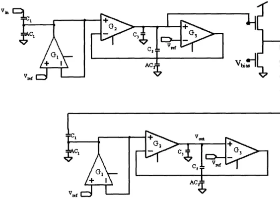
Figure 2.6: Block Diagram Of Capacitive Attenuation Filter With Offset Adaptation.. 55
Figure 2.7: Block Diagram of Single Capacitive-Attenuation Filter With Noise Sources
...
57
Figure 2.8: Experimental Transfer Function of Single Capacitive-Attenuator Filter... 60
Figure 2.9: Experimental Demonstration of Offset Adaptation Effect on Transfer
F unction ...
. . ....
61
Figure 2.10: Measured and Simulated Noise for Single Capacitive Attenuation Filter. 62
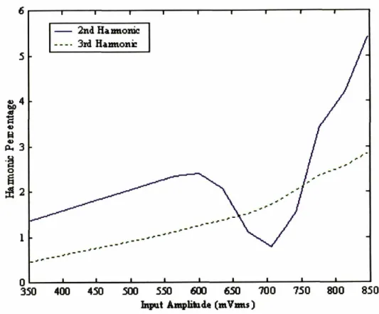
Figure 2.11: 2nd and 3rd Harmonics for Single Capacitive Attenuation Filter... 63
Figure 2.12: Two Interleaved Capacitive Attenuator Filters (One channel is shaded).. 64
Figure 2.13: Two Intertwined Transconductors...
65
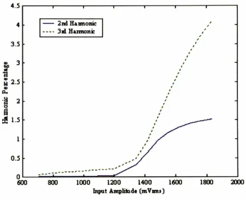
Figure 2.14: 2nd and 3rd Harmonics As A Function of Fundamental Amplitude For a
First-Order Differential Capacitive-Attenuation Filter... 67
Figure 2.15: Two Capacitive-Attenuation Filters With An Intermediate Source Follower
B u ffer ... 68
Figure 2.16: Fit Of First And Second Stage Outputs To Ideal Filter Transfer Functions
...
...
... 7...
70
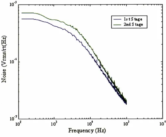
Figure 2.17: Noise In A Cascaded Differential Capacitive Attenuation Filter, After the
First Stage And At The O utput ... ... 71
Figure 2.18: Harmonic Distortion Measurements for The Cascaded Differential
Capacitive-Attenuation Filter... ... 72
Figure 2.19: Gain vs. Input Amplitude for the Cascaded Differential
Capacitive-A ttenuation Filter ...
72
Figure 2.20: Demonstration Of Programmability Of The Cascaded Differential
Capacitive-Attenuation Filter... ... 73
Figure 2.21: Bionic Ear Topology... ... 74
Figure 3.1: Experimental Example of Jump Resonance...
... 77
Figure 3.2: Basilar Membrane Measurements.
Figure used with permission from
Ruggero et. al. [17], copyright 2000, The National Academy of Sciences of the
U nited States of Am erica. ... ... 78
Figure 3.3: Two-Integrator Biquad. ... 81
Figure 3.4: Transconductor Implementation ...
...
... 81
Figure 3.5: Describing Function Block Diagram...
...
84
Figure 3.6: Fukuma-Matsubara Circles. ... 85
Figure 3.7: Fukuma-Matsubara Plots with Different Values of
Q...
.86
Figure 3.8: Graphical Operating Point Determination...
87
Figure 3.9: Jump Resonance in the Graphical Method ...
....
.89
Figure 3.10: Frequency Response for Different Values of g. ... ... 90
Figure 3.11: Loop gain Block Diagram. ... 91
Figure 3.12: L oop G ain Plot ... 92
Figure 3.13: Jump Resonance from Different Transconductors. ...
93
Figure 3.14: Experimentally Measured Frequency Sweeps and Simulation Results .... 94
Figure 3.15: Experimentally Measured Amplitude Sweeps with Simulation ... 95
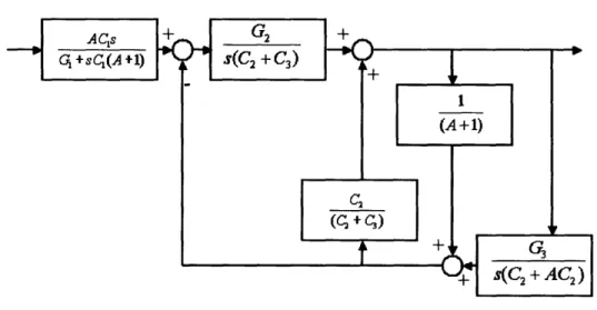
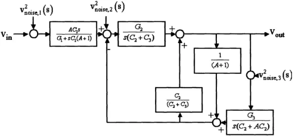
Figure 3.16: Feedback AQC System Block Diagram ...
... 96
Figure 3.17: Die Photograph of AQC Feedforward and Feedback System ... 97
Figure 3.18: Measured Open Loop Frequency Sweeps ... 98
Figure 3.19: Measured Feedback AQC Frequency Sweeps ...
98
Figure 3.20: Measured Feedback AQC Frequency Sweeps with Extended Range... 99
Figure 3.21: Feedforward AQC Block Diagram ...
100
Figure 3.22: Measured Feedforward AQC Frequency Sweeps with Extended Range.100
Figure 3.23: Jump Resonance Trajectories ...
102
Figure 3.24: Jump Resonance Frequency Sweep with State Space Method ...
102
Figure 3.25: Domains of Attraction for Jump Resonance... 103
Figure 3.26: Domains of Attraction at 30Hz for Different Phase...
... 104
Figure: 3.27 Domains of Attraction at 50Hz. ...
105
Figure 3.28: Experimental Measurement of Subharmonic Oscillations. The blue trace
is the input signal. The yellow trace is V, showing first and third subharmonic
content. The magenta trace,V
2, is predominately third subharmonic ... 106
Figure 3.29 Domains of Attraction at 75Hz...
...
106
Figure 4.1: Block diagram demonstrating the parallel channels. Sound enters at Vi, and
is first filtered by broad input filters. The filtered signals are then compressed.
A narrow bandpass filter selects a subset of these compressed frequencies. The
narrowband signal is then expanded...
118
Figure 4.2: Companding Test Cases ...
119
Figure 4.3: Companding channel block diagram. The signal enters at X
0. The signal is
filtered by the broadband filter to create X1
. The envelope detector creates the
envelope signal, X
1,. The power law circuit then applies a linear amplification in
the log domain to create Xp,. The output of the power law circuit, XP,, is
multiplied by the filtered signal, X,, to form a compressed signal, X,. The
expansion half channel performs simarily ...
120
Figure 4.4: Basic transconductor topology. The output current is proportional to the
differential input voltage...
123
Figure 4.5: Degenerated transconductor topology. This transconductor is shown to
lead to more power efficient filters ...
123
Figure 4.6: Degenerated transconductor with noise sources. The noise introduced by
each transistor can be modeled as a noise current source in parallel with the
transistor. The total output current noise can be calculated by adding the power
contributions from each noise source ...
124
Figure 4.7: Basic filter topology.
Two transconductors are combined with two
capacitors to form this bandpass filter ...
126
Figure 4.8: Basic filter block diagram. The feedback found in the filter in Fig. 6 can be
seen clearly in this block diagram ...
127
Figure 4.9: Cascaded filters. Two filters are cascaded to create second-order roll-off. A
buffer is inserted between the filters to prevent loading... 128
Figure 4.10: Envelope detector topology. This topology was developed by Zhak in [10].
...
13 2
Figure 4.11: Drive transconductor topology. M
9provides shifted outputs... 133
Figure 4.12: Peak detector circuit. This circuit was developed by Zhak et. al [10].
Currents are filtered with an attack time constant set by Ia& and a release time
constant set by I,, ...
135
Figure 4.13: Power law circuit. This circuit was developed by Baker et. al. in [8]. The
logarithm of the input current is taken by M,. A current is generated by Gi
comparing log(Ii) to log(If,,fl). This current is converted to a voltage by Gon
t.The output current is then related to the input current by a power law... 136
Figure 4.14: Variable gain amplifier circuit. This is a subset of Fig. 12. Here two
transconductors are used to provide a continuously variable gain ...
138
Figure 4.15: Compression half channel block diagram. To perform compression, the
output of the power law cell is connected to the output transconductor of the
variable gain amplifier. In this configuration a small signal creates a small
output transconductance and high gain. ...
138
Figure 4.16: Expansion half channel block diagram. The expansion half channel differs
from the compression half channel only in the connection of the output of the
power law cell to the variable gain amplifier. In the expansion half channel, a
small signal creates a small input transconductance in the variable gain
amplifier leading to a small gain...
141
Figure 4.17: Resistive divider biasing. This conservative technique uses voltages to bias
transistors used as current sources at each channel. Resistors placed along the
line create a voltage divider.
The constant voltage division between the
channels leads to an exponential division of currents ...
142
Figure 4.18: Programmable channel summer. The transconductor at the output of each
channel creates a current proportional to the difference between the channel
output and Vo.
This creates an average of the channel outputs weighted by the
D A C values. ...
143
Figure 4.19: Programming shift register. The programmable shift register reduces the
number of wires required to program the chip. Data is shifted into the register
from a data pin using a clock pin for timing. A third pin causes the chip to store
the data in the latch associated with the correct DAC and channel. ... 143
Figure 4.20: Companding system chip die photograph. This chip was built on AMI's
0.5um process through MOSIS ...
144
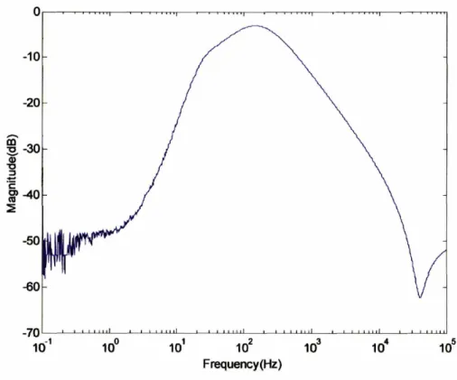
Figure 4.21: Filter frequency response. The bandpass filter is well behaved with
second-order roll-off on both sides. ...
145
Figure 4.22: Filter frequency response at high values of q, Mismatch between the two
stages of filtering degrades filter performance when q>10 ...
146
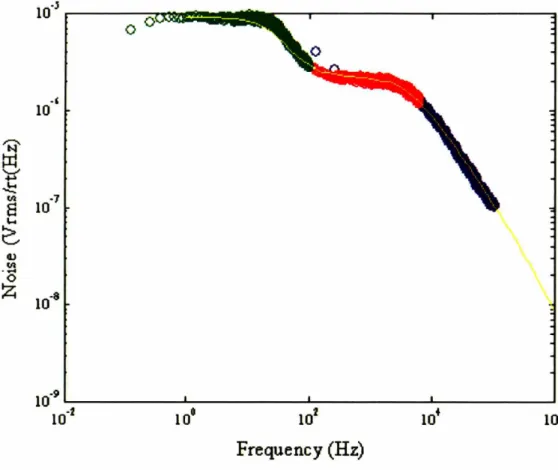
Figure 4.23: Filter noise.
The experimental measurement agrees well with the
calculated prediction in the passband, but the output buffer introduces excess
noise at high frequencies... 147
Figure 4.24: Distortion measurement. The linear range is limited by both second and
third harmonics when the fundamental amplitude is approximately 50mVrms.
...
14 7
Figure 4.25: Dynamic range versus q, The dynamic range is the difference between the
noise and the linear range. This plot shows that the noise changes very little
with qf while the linear range decreases significantly...
148
Figure 4.26: Envelope detector linearity. The output current of the envelope detector is
linear with the input voltage amplitude over greater than 40dB variation ... 149
Figure 4.27: Dynamic range at 250Hz. The input-output characteristics of the envelope
detector are plotted for three different values of the input transconductance.
The effect of the deadzone at small amplitudes can be seen only in the lowest
bias condition when ED n=2.0V and the transconductor is biased at
approxim ately 300pA ...
150
Figure 4.28: Dynamic range at 5kHz. The same experiment as Fig. 26 was performed
here with the channel frequency at 5kHz. The higher frequencies makes the
deadzone a bigger problem ...
150
Figure 4.29: Square wave modulated sine wave. This signal is used to test the dynamic
response of the peak detector. ...
151
Figure 4.30: Peak detector release times.
This figure shows the output of the
compression half channel. The system is compressing the input to a constant
amplitude. In response to a step down in amplitude, the system increases the
gain as the peak detector output decays. This provides a measurement of the
peak detector release time constants. The time constants in this figure are: 5ms
(A), 10ms (B), and 20ms (C) ...
152
Figure 4.31: Adjustable compression curves. The output amplitude was measured
using a lockin amplifier while the input amplitude was swept. The four curves
were taken with different values of the companding index, n,, from 1 to 0.5... 153
Figure 4.32: Compression curves measured with a low pivot point. Compression curves
were measured as in Fig. 30, but with I•f,i set to a low value. This biasing
lowers the pivot point of the compression curves and limits the linear range of
excursions on the high side. This nonlinearity shows up in the curvature of the
curves even at low amplitude ...
154
Figure 4.33: Two-Tone Suppression as a Function of Suppressor Amplitude. (A) is a
plot from simulation taken from [2]. (B) is experimental data from this chip.
The amplitude of a, was kept constant for each curve while the amplitude of a
suppressor tone, a
2, was swept. As the suppressor tone increase in amplitude, it
suppressed the test tone ...
155
Figure 4.34: Two-Tone Suppression Versus Suppressor Amplitude. (A) is a plot from
simulation taken from [2]. (B) is experimental data from this chip. The degree
of suppression was determined by the companding index. na. ... 156
Figure 4.35: Two-tone suppression versus frequency. (A) is a simulation from [2]. (B)
is experimental data from this chip. The power at the output of the channel was
measured while the frequency of the suppressor tone was swept. When the
suppressor tone was far from the center frequency the suppressed tone set the
amplitude. As the suppressor approached the suppressed tone, suppression
reduced the power at the output. Then when the suppressor tone was within the
narrow filter bandwidth the powerful suppressor tone was transmitted to the
output causing the peak ...
157
Figure 4.36: Two-tone suppression versus q,.
(A) is a simulation from [2].
(B) is
experimental data from this chip ...
157
Figure 4.37: Two-tone suppression versus q2. (A) is a simulation from [2]. (B) is data
from this chip ...
...
158
Figure 4.38: Noise Suppression From 1kHz Tone...
159
Figure 4.39: Revised Expansion Topology...
160
Acknowledgements
Throughout my graduate school career, I have received a great deal of help from a great many people. This thesis and more importantly my skills and views on engineering and academia have been enormously shaped by my advisor. The act of preparing this document has reminded me of how much I have grown during the time in his group.
That group has also been very important. My closest research interactions have been with the cochlear implant team. Michael Baker has taught me a great deal about automatic gain controls and even more about his style of lab work. I hope that I have learned a small bit of the perseverance that Ji-Jon Sit demonstrated in tackling system design issues on the cochlear project. Serhii Zhak frequently reminds me to tackle even the most difficult of math problems that arise in circuit design. Finally, Lorenzo Turicchia has shown a combination of patience and curiosity that have served him very well.
Beyond the cochlear implant group, I have also learned a great deal and received a large amount of help over the years. I am slowly developing an attention to detail following the example of Micah O'Halloran who has lent me his time and attention on multiple occasions. Likewise, Soumyajit Mandal has offered his breadth of knowledge many times.
Outside of work, I have had the support of a great collection of family and friends. My parents and sister have humored my constant claims and complaints of graduate student poverty. My friends from college (Allen Chen, Julie Wertz, Joe Pacheco, Steve Sell, Shonna Coffey, Venetia Chan, and Andrew Singleton) have stood by me even when I did not respond to emails. My friends from dragon boat (Jason Tom, Jonathan Scherer, and many others) have provided a view of the world beyond graduate school. Finally, my beloved girlfriend Xiuning Le has put up with the worst of my graduate school experience as I have tried to find a job and graduate.
Biographical Note
Christopher Salthouse received his bachelor's and master's degrees in Electrical Engineering from the Massachusetts Institute of Technology in 2000. His master's thesis, Improvements to the
Non-Intrusive Load Monitor, was supervised by Prof. Steven Leeb in the Laboratory of
Electromagnetic and Electronic Systems at M.I.T. He has worked for the last six years for Prof. Rahul Sarpeshkar in the Research Laboratory of Electronics at M.I.T. He has also been on the teaching staff for 6.002 Introduction to Electronic Circuits and 6.973 Analog VLSI and Biological Systems. He has presented his work at the International Symposium on Circuits and Systems and in the Journal of Solid State Circuits and the IEEE Transactions on Circuits and Systems I.
Chapter 1: Introduction
Filters are one of the basic building blocks of analog circuits. For decades, researchers have studied electronic filters [1]. So much is understood about filter design that one popular introductory textbook tells readers, "Filter design is one of the very few areas of engineering for which a complete design theory exists, starting from specification and ending with a circuit realization [2]." While this quote may be true for linear filter design, it remains untrue for the non-linear regime. For small signals, filters can be approximated by linear models, but as signals grow this approximation weakens. The range of signals for which the approximation holds is the dynamic range. It is the range, measured in dB, between the smallest signal the system can process and the largest. Every filter has some signal that is so small that it cannot be distinguished from noise and some signal so large that the filter does not perform properly. This thesis is about the second half of that sentence, defining the high end of analog filters for audio applications.
This thesis is divided into five chapters. The first chapter provides a background of technologies used in analog filtering in the audio frequency range. The second chapter presents my work on the capacitive-attenuation technique for increasing the linear range of gm-c filters. The third chapter explores jump resonance, a non-linear behavior of filters, including my novel graphical analysis method and adaptive circuit solution. The fourth chapter describes the application of micropower analog filters to my companding speech processor to improve speech recognition for the hearing impaired in moderate noise environments.
Section 1. Audio Filter Applications
There are a variety of applications for audio filtering including: automatic speech recognition, speech enhancement, speech coding, and processing for cochlear implants. In each of these applications, the filters are not required to be linear, but must demonstrate some of the properties that are guaranteed by linearity. So, linearity is often used as a proxy for the properties that are needed. So, I will first analyze the requirements for linearity and then look at the places where these requirements can be relaxed for the applications of interest.
Automatic speech recognition has been the topic of much research in the last half century. A
general architecture has emerged. Phonemes are extracted and then the sequence of phonemes
is interpreted. Because phonemes are defined by spectral features such as formants, the
phoneme detection stage involves filtering as either an explicit or implied process. In some
designs, the speech is separated into frequency bands by a bank of bandpass filters. Formants
are then extracted by measuring the power in each band. Alternatively, the two processes can
be combined in the digital domain using a Fast Fourier Transform (FFT) or Linear Predictive
Coding (LPC). LPC finds a function that predicts the next sample value based on a series of
previous samples. Because this is equivalent to defining a discrete time filter for the channel,
the LPC is often accomplished by first transforming the samples to the frequency domain,
although some algorithms function solely in the time domain [3]. After the phonemes are
extracted, they are matched to possible words. Then the possible words are weighted based on
sentence level probabilities. In these systems, the phoneme identification may be amenable to
analog signal processing while the later classification steps are probably more appropriate for
digital computation.
One of the most visible areas of research in audio processing has been perceptual coding. The
factor of 10 compression achieved in MP3 encoding is in large part due to these encoding
techniques that perform selective compression based on the ability of humans to hear the
artifacts. The encoding process can be divided into two stages: perceptual modeling and
variable compression. In the perceptual modeling stage, a frequency analysis is performed on a
window of the sound and a masking profile is created. This masking profile is then used to set
the maximum errors when each frequency band is compressed
[4-5].
This masking profile can
be developed using special analog filters, while the variable compression is performed with
digital computation.
Speech enhancement is a related area that has shown some success and promises even more.
Speech enhancement is the general term for a variety of techniques used to improve theintelligibility of speech for either human or computer listeners. The basis of these methods is
amplifying those parts of the signal, as defined in time and frequency, which have a high signal
to noise ratio while attenuating those portions where the noise dominates. One of the simpler
algorithms performs non-linear expansion based on signal amplitude in each frequency band
[6]. More advanced techniques use adaptive filtering such as Kalman filters to maximize the signal to noise ratio based on noise estimates measured during pauses in speech signals [7]. Spectral Subtraction lies somewhere between these systems in complexity, with frequency domain subtraction of the noise signal from the composite signal [8]. The performance of these systems is often characterized by resulting SNR, but work has also been done comparing the automatic speech recognition scores on the output of these systems [8]. These systems have been implemented in both DSP and analog systems.
While the above applications are aimed at a broad audience, the hearing impaired can benefit even more from audio frequency filters. It is estimated that one million Americans are sensorineurally deaf. They can only hear with the aid of a cochlear implant, a biomedical device that directly stimulates the nerves in the cochlea in response to sound [9]. A microphone captures the sound. Then the dynamic range is decreased using an automatic gain control. The sound is divided in to frequency bands. The power in those bands is calculated. A second stage of compression is applied. Finally, the neurons are stimulated [10-11]. Active research on cochlear implants is aimed at optimizing the compression strategy and minimizing the power consumption to extend battery life.
Section 2. Analog Filter Topologies
In any of these applications, micropower analog filters are generally built in one of two technologies: Gm-C and log domain. Both of these technologies include a variety of topologies. The Gm-C domain is defined as filters built using linear voltage to current converters, the Gm, and capacitors, the C. These filters are also frequently referred to as OTA-C filters. Log domain filters differ in that they store state on capacitors which contain a log representation of the signal and use exponential voltage to current converters. They go by many names including: Exponential State Space (ESS), Dynamic Translinear (DTL), and Bernoulli cells.
A: Gm-C
Sanchez-Sinencio and Silva-Martinez provided an excellent overview of Gm-C filters in greater depth than presented here [12]. Research in Gm-C filters addresses both the transconductor
design and the filter topology. A survey of the options available in each and the tradeoffs associated with them is presented here.
Single Ended
Practical transconductors are either single transistor input trans conductors or differential pair transconductors. Single transistor input transconductors can be built using saturation region
MOSFETs, triode region MOSFETs, or forward active region bipolar transistors. The
saturation MOSFETs and active bipolar transistors have the advantage of yielding the simplest possible circuits. Each transconductor is one transistor. The disadvantage of this design is the limited linear range. In fact, it is not linear at all as shown in Fig. 1.1. In subthreshold operation, the transistor curve is exponential. Above threshold, it is a square law. For small signal swings, it can be approximated by a linear function [13].
12 - Transistor - Linear Approximation 10 8
..
2o
0... 0.46 0..t8 0.5 0.52 0.5.-VoltageFigure 1.1: Linear Approximation ofa Single Saturated Transistor
Triode transconductors offer improved linearity. One commonly used approximation for the current in a MOSFET when the gate-source potential is strong enough to create strong inversion, but the drain-source voltage is small enough that the device is not is saturation is
given by
Eq. 1.1[14].
I
DS ~ :.uC~ [(V
GS -V",)V
ns - ~V;"]
(1.1)If CJ. is small, the drain current is proportional to the drain-source voltage with the
proportionality defineu
by
the gate voltage. In fact, this technique has been usedextensively [15-17]. Sample curves from simulation are shown in Fig. 1.2. The linear range at the bottom is limited by the threshold voltage and at the top by the input signal. Because this is based on above-threshold transistors, the current levels are difficult to achieve below the order of microAmps. Unlike the saturation mode transconductor, the triode mode transconductor requires additional circuitry to maintain the operating condition as shown in Fig. 1.3.
Figure 1.2: Triode Region Transconductor Simulations
VDS
Figure 1.3: Triode Transconductor Circuit
Differential
Differential transconductors are the other broad class of transconductor circuits. The simplest implementation is shown in Fig. 1.4. Transistors M, and M2 split the current, Ibia, , between the
two legs. The current mirror formed by M3 and M4 performs the current subtraction to create
Iou,. The derivation of Iou, for subthreshold transistors is straightforward.
VDDoo
VH
Figure 1.4: Differential Transconductor Circuit
KV+-V,
I,=
Ie ;12=loa, = I, -12
Ibias
1 +12
out = biasHV
V_ -V,sIe o
( KV,-V, KKV-V,=Ise
-e
0
SKV,-V. , -V=I(e 0 +e
KV+ KVYee -e,
,V+ KKVet0 + eT
Iout= Ibias
tanh
( 21(1.2)
(1.3)
(1.4)
(1.5)
The linear range is 2 l/Ki , approximately 75mV.
The advantages of the differential pair are inherent differential operation and programming to very low transconductance. The differential operation ensures common mode rejection and cancellation of noise from bias currents. The low transconductance is achieved by programming the bias current as opposed to a DC gate bias for the single ended designs. Both of these properties can be compared to a pseudo-differential transconductor built by combining two singled ended transconductors and subtracting the output current of the inverting input [18]. This transconductor requires matching of two transconductances and the transconductors will continue to respond to the common mode requiring increased current.
Linear range is one of the major limitations with any of these saturation mode topologies, either single ended or differential. A wide variety of techniques have been used to improve this linear range, but most work has focused on attenuation and degeneration [12, 19].
(a) (b)
Figure 1.5: Attenuation Techniques For Differential Transconductors
Attenuation is the simplest of the techniques; the signal is simply scaled by a factor less than 1 prior to controlling the differential pair. Figure 1.5 shows a simple differential pair (a) and three attenuation methods (b-d). Resistive attenuation (1.5b) has been used in discrete OTAs, but is impractical for integrated circuits because of power and space limitations. A capacitive attenuator (1.5c) can be used for integrated circuits, but a DC path must be provided as discussed in Chapter 2. The final circuit (1.5d) is also an attenuation scheme, but with intrinsic attenuation. By using the well as the input to the circuit rather than the gate, the transconductance of the transistor is decreased. This is classified as an attenuation approach
t
F~i
because it is a feed-forward approach that is exactly equivalent to supplying a smaller signal. Physically, the classification of this approach as an attenuation scheme is justified by recognizing the surface potential of the transistor as the control terminal with capacitances from gate and well controlling this terminal [19].
D A
fr
J)
ho
C
(a)
(b)
Figure 1.6: Degeneration Techniques for Differential Transconductors
Degeneration schemes also lower the voltage across the control terminal, but they do it through feedback. Figure 1.6 shows three techniques for degeneration. In all three, the current at the output passes through the degenerating device creating a voltage that subtracts from the input voltage applied to the transconducting transistors. The circuit in part (a) has diode degeneration. The voltage across the diode connected transistor lowers the voltage on the source of the input PMOS, decreasing the current through the device. If the diode and transconducting devices are the same dimensions, they will split the input voltage evenly, doubling the linear range. This technique limits the common mode range of the circuit because the diodes are continually dropping voltage across them.
Because it is only the differential mode where degeneration is required, circuits such as the one shown in part (b) are often used. No common mode current flows through the degenerating device, but any imbalance between the two legs is fed through the degenerating device creating a voltage imbalance that functions as in part (a).
The final example of degeneration presented here (c) is a combination of source and gate degeneration. The voltage induced across the diode connected transistor lowers the voltage on both the source and the gate. Both terminals act to lower the current [19].
B: Log-Domain Filters
Unlike transconductance filters, log domain filters do not approximate the transistor as a linear element. Instead, the transistor is used as an exponential device. This is demonstrated for a bipolar transistor and a subthreshold MOSFET in Fig. 1.7 and Eq. 1.7 and 1.8.
Id
VI
V
gs
OW
(a)
(b)
Figure 1.7: Exponential Devices: (a) is described by Eq. 7. (b) is described by Eq. 8.
Vbe
Ic = Iq,e (1.7)
Id=
Io.,e 0
(1.8)As with transconductor filters, there are a variety of design methods that are used to generate log domain filters. Three of the most published techniques are associated with the keywords Exponential State Space (ESS), Dynamic Trans Linear (DTL), and Bernoulli Cell.
Exponential State Space
Much of the excitement about log domain filtering began with a series of papers by Frey on what he termed Exponential State Space filters [20]. The ESS method begins with a state space description of the desired filter such as the second order system in Eq. 1.9.
S0 2
0
(1.9)
Y
=
1/Q 01
x2
Then the exponential mapping, Eq. 1.10, is applied.
f (VI) = x,
(1.10)
This transforms the generic state space description to the form in Eq. 1.11.
F'(V) = AF(V)+ BU
(1.11)
Y = CF (V)+DU
Using the bipolar equation (Eq. 1.7) to transform the filter equations (Eq. 1.9) gives Eq. 1.12.
L,
= 0- I, - O I, + O U
(1.12)
CA -=C CC ) t + C° UQ
I
I,
(1.13)
2Ic 2 -ý
= C 2 0
)00, 1 2
In this form, it can be seen that the two equations define currents onto capacitors C, and C2.
The first term is a constant current source; in general the terms involve division of currents. Because the currents are derived from an exponential function of voltage, this division can be accomplished by subtraction of voltage. Some of the building block circuits used by Frey are shown in Fig. 1.8. The first two use a combination of n-type and p-type transistors while the third has been proposed for higher frequency applications since it only requires n-type transistors [19-20].
(b)
Figure 1.8: Frey's ESS Units
ClQo)t
Q
Vdc
'.lwO't
I
0CQ
Figure 1.9: ESS FilterC
2 taThese blocks are then used to build up the circuit for the filter as shown in Fig. 1.9. In practice, this circuit will not work because of the DC operating point. C2 is only connected to a current
source with no current sinks. The operating point can be adjusted by adding an additional input to the state space representation. Because the filter is linear, a DC value applied to this input will simply shift the output. Equation 1.9 becomes
S
-o/Q
-o
0
x
1+
0
UDC(1.14)
Any negative value of UDc will give a viable operating point, but it is straightforward to solve for the required input current to set x, and x2 to the same value. If the primary input offset is
IDC, then the DC input should be
IQ
.
Adding this to the circuit creates the circuit in Fig.Q+1
1.10.
CIQMOt
Q
Figure 1.10: Improved ESS Filter
Dynamic Trans Linear
The Dynamic Trans Linear (DTL) technique views log domain circuits as a generalization of translinear circuits. The basic building block is shown in Fig. 1.11 [22]. This block can be simply analyzed. V Iq = Ie4 (1.15) Icap
=CV
(1.16) q Ie=V(1.17)
At Atvdc
Figure 1.11: DTL Building Block
Equation 1.18 is the standard equation used in this method.
Eq. 1.14 can be represented in the current domain as Eq. 19.
I"2
-
I i
2
2
The state space description in
0
U +
IDC
OO
(1.19)
Y
=1/Q
01
The
current on to capacitorsC,
and C2 canbe
solved by manipulating Eq. 1.19.IcH
=
CI
=
C
2 0 U
S=C201212
12
These equations can be implemented using Gilbert multipliers as shown in Fig. 1.12.
(1.20)
cap
CI(Oo4t Q
Figure 1.12: DTL Filter
The transistor count can be reduced by factoring the multiplications in Eq. 1.20 to write them as Eq. 1.21
S,
c (1.21)Ic, =
C2
t2
,-
IDC2 0
The two multipliers that feed C, are partially combined, as are the two multipliers that feed C2.
ClQ
Q
Figure 1.13: Improved DTL Filter
The DTL technique is primarily an analysis technique and applies to any circuit where the linear state variable is a current stored as a base-emitter voltage, Vbe, on a capacitor. So, other DTL circuits could also be built to realize this system response. But, this design is a useful example
for comparing the different techniques, as is done following the Bernoulli Cell technique.
Bernoulli Cell
The Bernoulli Cell based transconductors are based on the building block shown in Fig. 1.14. Quite simply, a capacitor is placed at the emitter of a transistor. This is remarkably similar to the building block used for DTL circuits, where the capacitor is placed on the base of the transistor. In fact, practical Bernoulli Cells circuits can be analyzed using the DTL principle.
The DTL analysis cannot be applied to this building block cell, however, because the voltage difference between the base and emitter of the transistor are varying. In comparing the building block to the DTL building block, the two primary differences are the negative sign in the exponent because of control of the transistor through the emitter, and the inclusion of transistor current in the capacitor current, Icap
Vb
P
C
Figure 1.14: Bernoulli Cell Building Block
Iq = Ie (1.22) - (1.23) CV = Icap (1.25)
-q
= -(1.26)
II
Cq
IqC q IqC , = IIq - I (1.27) IqC, = If I -I ( 1.28)Following the same flow of analysis that was used for the DTL system in Eq. 1.15 through 1.20, it is clear that this system is different. This circuit is called a Bernoulli Cell because this equation is of the Bernoulli form [23]. Mathematicians suggest that this circuit can be linearized by making the substitution in Eq. 1.29.
1
T--
(1.29)
Circuit designers should recognize this substitution as the conversion from emitter voltage to
base voltage. The negative sign in the exponent represents this reciprocal. The substitution
continues with Eq. 1.30-1.32.
T -
(1.30)(1.31)
T
1
If
T2
T
2T
TC, =I-TI, (1.32)
The form of Eq. 1.32 shows that this structure has less flexibility than the techniques presented earlier. It is easier to see this limitation if a filter is built using this building block. The simplest filter uses just one of these building blocks. Even with this constraint, multiple filters may be built two are presented in Fig. 1.15. Circuit A is from [23] and Circuit B is from [24].
Dut
out
Figure 1.15: Bernoulli Cell Filters
Iow, as a function of I,, is derived in Eq. 33-44. The translinear principle, called the static
translinear principle by the DTL practitioners, is used to generate Eq. 1.33.
I l i I
I
j -inThe transistor relation is then used to generate
Iq=Ie,
e
(1.34)
And the capacitor relation is used.
CV =
Iq-
If(1.35)
I
S- = Vb -V ((1.36) " = i V (1.37)q,
in
Ot -Lq = Ot 'in - . (1.38)q
inC
q I= I-I
(1.39)
Then Eq. 1.33 is substitute into Eq. 1.39.
1,,I,
i,,Io
Iq=
inf
In f ou(1.40)
out out
Cot
=Co
Lin+/I - ---
(1.41)
I, 'out
( lin in out
____I I., II
In in out
Cot iout Iou, If - Iin If
(1.43)
out I (1.44)
I,, If + sC t
With a complete circuit as in Fig. 1.15, it is possible to use the DTL principle for analysis. The network that linearizes the Bernoulli Cell may also be viewed as creating a DTL circuit. The
base of the output transistor is driven by a level shifted version of the capacitor current. From Eq. 1.18 in the DTL section,
ut= -cap
(1.45)
ou
cot
Substituting in for Icap yieldsj
out-I
q-If
(1.46)
IoU, cq,
Equation 1.33 can be used to remove Iq from the equation.
ut_ Iinf if (1.47)
Iou coIoU, co,
'oucot = ,,,I - Iu out (1.48)
out f (1.49)
I,, I, +sCo
Log Domain Filter Comparison
From Eq. 1.49 the loss of generality in the Bernoulli Cell method as compared to ESS and DTL is clear. This building block is simply a first order low pass filter. These blocks can be combined to make general purpose filters, but the added overhead can be significant. Figures 1.10 and 1.13 show that the ESS and DTL methods create similar circuits. Since the Bernoulli cell is a subset of DTL, it is simply an option when the circuit being built fits the requisite form.
Class-AB Operation of Log Domain Filters
In the log domain circuits presented so far, the signal can not exceed the bias current, but log domain circuits can be operated in a class-AB mode to increase the maximum signal [25]. This maximum amplitude is similar to the transconductance requirement that transconductors be biased with a current equal to their maximum current. But, the limitations for the linear range are very different between Gm-C and log domain circuits. For Gm-C filters, as the signal grows it begins to clip on both the top and the bottom as shown in part (c) of Fig. 1.16, but with log domain circuits the signals only clip on the bottom as in part (b). Signals can be processed without clipping even if they are much larger than the bias current, as long as they never become negative.
a)
VV
b)
Figure 1.16: Clipping
This property of log-domain filters allows the creation of a special type of differential filters. As with other differential systems, the composite variable is the difference of the signals in two paths. But, rather than keeping the sum of the two constant, a rule is created such that both currents are always positive. A common rule is that the product of the two variables is constant. Figure 1.17 demonstrates the difference. Part (a) shows the differential signals in a constant common mode differential scheme. Part (b) shows the differential signals used in a class-AB scheme.
A A A /
a)
IVVV
b)
Figure 1.17: Differential Signals: a) Constant Common Mode. b) Class AB
This technique works for the same reason as other differential techniques. Any common mode effects are canceled out when passed through identical linear systems. So, a particularly useful common mode is chosen for this application. Whereas a constant common mode approach doubles the linear range, since the maximum swing of two channels are now added to each other, the class-AB approach can increase the linear range by much larger amounts.
Ultimately it is limited by the assumptions of identical linear systems and the ability of the input circuit to create the signals. This distortion is well modeled by the distortion in a simple current
v v v
mirror. As the current increases, some of the current is used to charge up the gate capacitance. As the current decreases, this capacitance is discharged through the transconductance of the input device. If this current mirror is driven by a square wave, the output will not follow the falling edge. The distortion introduced by this pole is shown in Fig. 1.18 which limits the modulation index to approximately a factor of 5.
10 20 30 40 50
Modulation Index
Figure 1.18: The signal distortion introduced by the input circuit increases with modulation index, the ratio of the signal maximum to the geometric mean of the channels.
Section 3. Standard Dynamic Range Measurement Techniques
The high end of dynamic range of filters is defined differently for different applications. For generic filter design, total harmonic distortion (THD) is the most often used measure [26-28]. But, the THD level that defines the top of the dynamic range also differs with little explanation as to the chosen percentage. In communications systems, other standards are often used
[29-31]. Intermodulation distortion (IMD) is designed as a test of how the system performs with real world signals. More abstract measures include compression and intercept points.
A: Total Harmonic Distortion
Harmonic distortion is the generation of signals at harmonics of the input. Non-linear functions generate these harmonics as shown in Eq. 45- 48. Given the input signal
x(t)
=
A cos
wt
(1.50)
and a system described by the function
y(t) = ax (t) + ax2 (t) + a3 (t)
(1.51)
the output isy(t) = a A cos cot
+
a
2A
2cos
2ct +
3A
3cos
3cot
(1.52)
This can be simplified to
yt 2a
2 +4
A2 33a(1.53)
+ cos 2ct + cos 3cot
2 4
Total Harmonic Distortion (THD) is just the ratio of the power in all of the harmonics versus the fundamental [31]. There are two problems with this approach. The first is that the harmonics are filtered in later stages. So the system may display other non-linear qualities, such as gain compression discussed below, while not having significant harmonics. The other problem is that harmonic distortion becomes imprecise for systems that are moderately non-linear. A square wave has only 11% third harmonic distortion as measured in power.
B: Compression Point
An alternative to harmonics is to look at the gain of the system. Most systems begin to saturate as they become non-linear as shown in Fig. 1.16. In differential designs that rely upon common mode features canceling out, such as the class-AB topology, compression can introduce differential artifacts.
Section 4. The Auditory System
In building audio processing systems, it is natural to look at how the human auditory system functions as a reference design. The design is not being copied as a whole, so key features may be lost. For instance, non-linearity in the auditory system may be acceptable because of the massive parallel nature of the auditory nerve. But, it also may be a result of the redundancy in speech signals. Because of this, the non-linearity of the auditory system is considered.
A brief overview of the auditory system is useful for understanding the data. The outer ear consists of the pinna and the ear canal; together they gather sound and provide directionality cues. The middle ear serves as an impedance transformer to couple sounds from the air to the liquid in the inner ear. The inner ear, or cochlea, amplifies the sounds and divides it up in to different frequency bands. Different frequencies then stimulate different nerve fibers which head to the brain. Additional processing takes places in the brain at the auditory cortex and in the cochlear nucleus.
To quantify some of these effects, two important types of data are examined here. In the cochlea, the basilar membrane moves up and down with the sound wave. The movements of this membrane make up one large set of the data. The other set of data is taken from the auditory nerve. The nerves that carry signals from the cochlea to the brain can be recorded. Data from the two sources is now believed to show agreement [32].
A: Total Harmonic Distortion
Prof. Dallos measured the harmonics in the auditory nerve fibers. The frequency of excitation was swept to find the peak response or "best frequency." Then the output of the hair cells was measured. Because the signal on the nerve fiber is made up of spikes, a large number of samples are taken and averaged together to form a composite signal. Then the Fourier analysis of the composite signal is taken to measure the harmonic content. At 30dB SPL, a sound level corresponding to a whisper, the harmonics are all between -40dB and -50dB with respect to the fundamental. This roughly 1% distortion level corresponds to the values used to define the maximum linear range in many analog filters. But, for sound levels corresponding to normal
speech, 50dB to 70dB, the third harmonic peak is near -20dB. Ten percent distortion is far from linear. [33]. ! 1 U U, U U
E
E
0 000101• 1 O~o C, 1 t l t 0 2 4 6 8 10 12Frequency
(kHz)
FIGURE 3.4. Basilar membrane velocity scaled by input sound pressure for a number of sound levels. Vertical overlap of the curves indicates linearity of the response. At lower frequencies. the curves align within approximately a factor of 2. and are characterized as being essentially linear. By contrast, in the region of the characteristic frequency (CF), the response is remarkably nonlinear. (Data from Ruggero. Rich. and Recio 1992.)
Figure 1.19: Basilar Membrane Non-Linearity, used with permission of Ruggero.
B: Other Nonlinear Effects
In addition to harmonic distortion, the auditory system demonstrates other behaviors that are non-linear. Figure 1.19 demonstrates the changing frequency response with amplitude. It shows the movement of the basilar membrane at one location as frequency and amplitude are varied. The Q decreases significantly and the center frequency decreases as the amplitude increases. Masking is the broad term for behavior in the auditory system where the presence of one sound prevents the listener from hearing another sound. This includes the non-linear effect called suppression. These effects are similar to desensitivity and blocking in RF systems, but occur at amplitudes where the system normally operates.
Section 5. Companding Speech Processor
Some of these nonlinear effects can be implemented in analog filters. Turicchia has proposed a filter system that captures two-tone suppression behavior [34]. Cochlear models have been built in the past [19], but because of the complex interactions in these systems, they can be
42
difficult to customize to applications such as speech processor front ends or cochlear implants. This simpler system shows promise for these applications.
Filter
Filter
Figure 1.20: Companding Speech Processor
Turicchia's system is depicted in Fig. 1.20. A broad filter defines the frequencies that will influence the suppression. Then, non-linear compression is performed. A second filter selects the frequencies of interest. Then these frequencies are expanded.
This system can be well understood by examining a series of simple examples. For each of these examples, the system is set up to compress with the fifth root, n, = 0.2, and then expand to the fifth power, n2 = 1. Initially, it is assumed that the frequencies being observed pass
through both filters with no gain or attenuation. First, an input composed of a single sine wave of amplitude 1 is considered.
x
0= 1 sin (wt)
The output of the compressor is the same as the input.
x
2=x
0= lsin(wt)
And the output of the expander is the same as the input as well.
x
4=
x
= lsin
(wt)
A second possible input is a sine wave with an amplitude of 0.01.
x
0= 0.01sin(ot)
The compressor compresses the range of amplitudes by increasing this amplitude. 43
(1.54)
(1.55)
(1.56)
(1.57)
x2
k
0.4 sin
(0t)
(1.58)
Then the expander expands the range of amplitudes to recreate the original signal.
x4
= x
0= 0.01sin(0t)
(1.59)
Both of these signals pass through the system with no amplitude change. The nonlinearities cancel for signals that are passed through both filters. Suppression occurs in more complicated signals where part of the signal is present in the compression stage, but removed before the expansion stage. A signal composed of the sum of the two earlier signals may be considered.
x
0= Isin (ct)
+ 0.01sin (wo
2t)
(1.60)
The envelope of this signal is approximately 1, so the compression gain is one. And similar to
Eq. 1.55,
x2
= x
0= Isin(aot)+ 0.01sin (at
)(1.61)
If the second filter, G, removes the component at w, then
x
3= 0.01sin (0
2t)
(1.62)
The expansion step further decreases this amplitude.
x4
= 10
- '0sin(a
2t)
(1.63)
As in the biological cochlea, the gain control mechanism responds to large frequency components at nearby frequencies. When these are later filtered out, the small signal is smaller than it would have been had it been processed in the absence of the large signal.
This companding system is currently being tested by Turicchia in conjunction with collaborators for use as a preprocessor for cochlear implants and as a front end for a speech recognition system. To test the system for cochlear implant patients, he is working with Dr. Oxenham of the Auditory Perception and Cognition group at MIT's Research Laboratory of Electronics. Their experiment consists of sample sounds files that were recorded in a quiet environment. Noise is added to these samples. Then the companding processor is used to construct stimulation waveforms for each of the cochlear implant channels. In order to test the system with normal hearing subjects, a cochlear implant simulator is used to reconstruct audio samples. Subjects are presented the samples and given a forced choice.
![Figure 2.2: Harmonics from Bandpass Filter built using Wide Linear Range Transconductors (3]](https://thumb-eu.123doks.com/thumbv2/123doknet/13941485.451748/53.918.237.667.133.485/figure-harmonics-bandpass-filter-built-linear-range-transconductors.webp)

![[PDF] Les portails : créer et gérer un site web](data:image/gif;base64,R0lGODlhAQABAIAAAP///wAAACH5BAEAAAAALAAAAAABAAEAAAICRAEAOw==)